VLSI Korea
Inference Splits in Two: 5 Facts (SRAM Decode vs HBM)
AI inference is splitting in two: decode moves to HBM-free SRAM in NVIDIA's Groq 3 LPX, training stays on HBM capacity with AWS Trainium3. Five facts on the 57x bandwidth vs 162x capacity asymmetry, and Samsung on both sides. (As of Oct 24, 2026)


Inference Splits in Two: 5 Facts (SRAM Decode vs HBM)
AI inference is splitting in two: latency-sensitive decode is moving to SRAM chips with no HBM at all, while training and prefill stay on HBM capacity. (As of Oct 24, 2026)
30-Second Summary
- NVIDIA's Groq 3 LPX is in production. The LP30 chip carries 500 MB of on-die SRAM and 150 TB/s of SRAM bandwidth per chip, with no HBM (NVIDIA, announced at Hot Chips 2026, Aug 24-25, 2026).
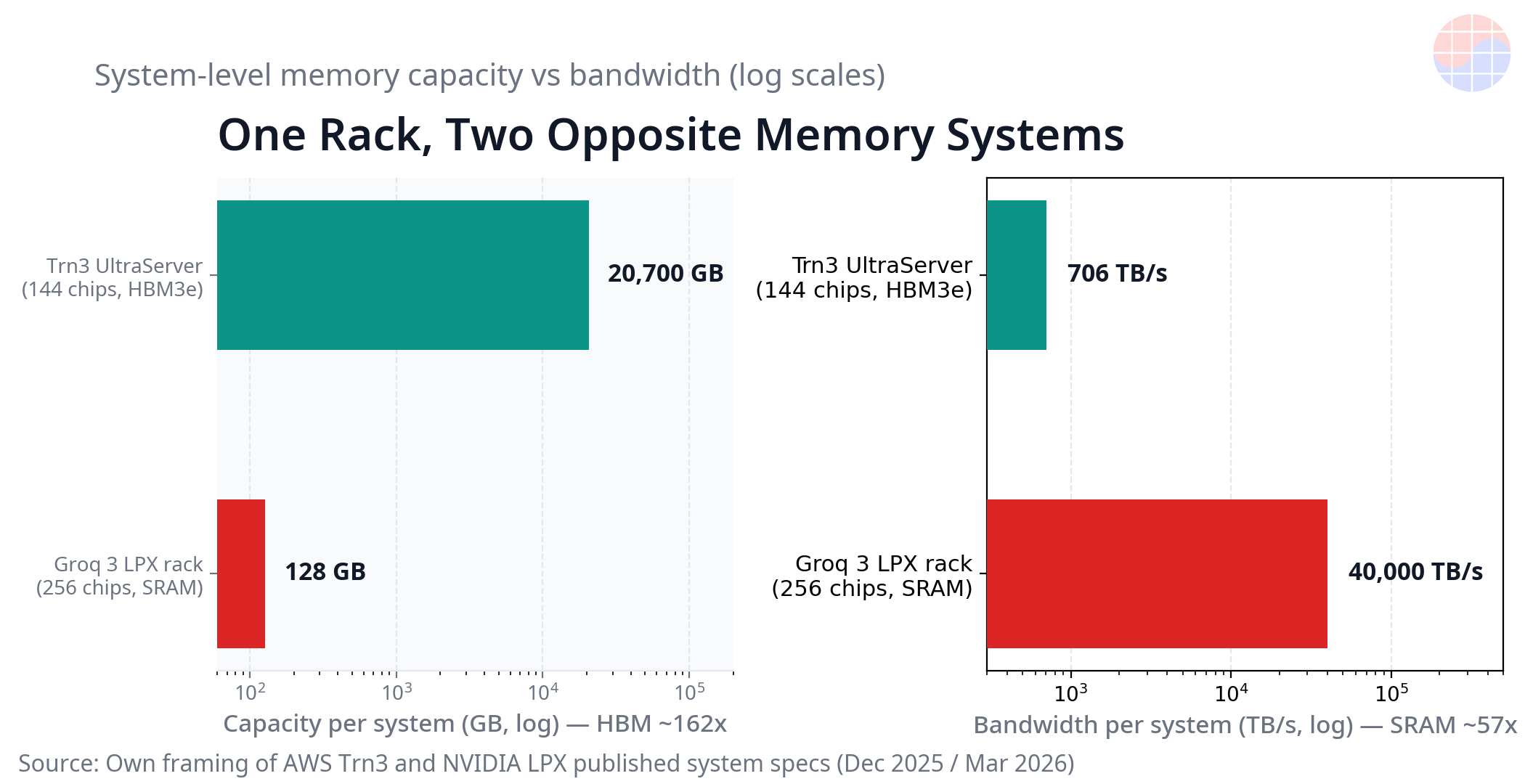
- By our own calculation, a rack of SRAM silicon delivers roughly 57x the memory bandwidth of an HBM rack, while the HBM rack holds roughly 162x the capacity. That asymmetry is the whole story.
- The training camp is consolidating around HBM capacity. AWS Trainium3 ships 144 GB of HBM3e per chip, and TorchNeuron, announced Oct 19, 2026, lowers the PyTorch porting barrier to training on Trainium (AWS).
- Samsung sits on both sides of the split: it is chasing HBM share in NVIDIA GPU platforms and is the sole foundry for the HBM-free LP30.
- SK hynix is the pure HBM-side exposure, but training demand underwrites near-term HBM volumes. SRAM caps only the latency-premium decode slice of the inference growth story.
Background
Inference has two phases with opposite physics. Prefill reads a long input context once and is bound by compute and memory capacity. Decode generates tokens one at a time, and every new token requires reading the full model weights again. Decode speed is therefore set, in practice, by memory bandwidth and latency.
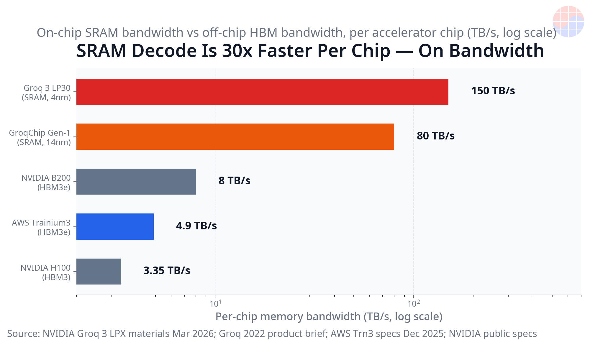
Until now, the GPU plus HBM combination has handled both phases. HBM offers large capacity, but it sits off-chip, which imposes physical limits on bandwidth and latency. SRAM sits on the die: its bandwidth is dramatically higher, but capacity is small and it consumes die area. The trade-off is not new. The first-generation GroqChip carried 230 MB of SRAM with up to 80 TB/s of on-die bandwidth (Groq 2022 product brief, vendor specifications), and Cerebras pushed the same SRAM-first philosophy to wafer scale with the WSE-3: 44 GB of on-chip SRAM and 21 PB/s of memory bandwidth (Cerebras published specifications, 2024). Both relied on compiler-scheduled, deterministic execution rather than runtime hardware arbitration.
What changed the structure was a licensing deal. On Dec 24, 2025, Groq announced a non-exclusive licensing agreement with NVIDIA. Founder Jonathan Ross, president Sunny Madra and other core team members joined NVIDIA, while Groq continues as an independent company under CEO Simon Edwards, and GroqCloud was not part of the deal (Groq announcement, Dec 24, 2025). The deal value of roughly USD 20B is a press report; NVIDIA has not disclosed a value, and it should always be read as reported, not confirmed.
Deep Dive: 5 Facts
- The LPX is in production, and the chip has no HBM. NVIDIA unveiled Groq 3 LPX at GTC in March 2026 and announced full production at Hot Chips 2026 (Aug 24-25, 2026). Per NVIDIA product and technical materials, the LP30 chip carries 500 MB of on-die SRAM, 150 TB/s of SRAM bandwidth, 96 chip-to-chip links at 112 Gbps, 2.5 TB/s of scale-up bandwidth per chip, and 350 ns chip-to-chip latency. A full LPX rack combines 256 chips in 32 trays for 128 GB of total SRAM, 40 PB/s of aggregate SRAM bandwidth, 640 TB/s of scale-up bandwidth, and 315 PFLOPS of FP8 inference compute. In NVIDIA's heterogeneous design, Rubin GPUs keep long-context prefill and decode attention, while the LPUs take the latency-sensitive feed-forward and MoE work inside decode; that is a vendor platform design, not a measured result. As a vendor claim, NVIDIA states up to 35x inference throughput per megawatt for trillion-parameter models when LPX is paired with Vera Rubin NVL72. The first third-party benchmark, run by Artificial Analysis on a pre-release Gemma 4 31B endpoint via Google Cloud at 100k-token context, concurrency 1, as the median of 50 sequential requests, measured 3,400 output tokens per second, roughly 4x the nearest alternative platform on that test (third-party result reported by NVIDIA). Those conditions matter: it is a single-user latency test, not a batched-throughput test. Nebius is the first LPX customer, and cloud availability runs through AWS, Google Cloud, Microsoft Azure and Oracle in the second half of 2026 (NVIDIA). Manufacturing sits with Samsung Foundry 4nm as sole manufacturer of the LP30. At GTC in March 2026, Jensen Huang said Samsung is manufacturing the Groq 3 LPU chip and that shipments would begin in the second half, probably around Q3; Samsung confirmed in June 2026 that it was producing the LP30. As reported on Oct 13, 2026, Samsung displayed a Groq LPU wafer at OCP 2026, with chips mass-produced on Samsung Foundry 4nm at Pyeongtaek (as of Oct 24, 2026).
- The bandwidth-versus-capacity asymmetry is the essence of the split (own calculation). Per chip, the LP30's 150 TB/s of SRAM bandwidth is roughly 31x the 4.9 TB/s of HBM3e bandwidth on Trainium3, and roughly 45x the 3.35 TB/s of an H100. At rack level, the LPX figure of 40 PB/s, or 40,000 TB/s, is roughly 57x the 706 TB/s aggregate bandwidth of a Trn3 UltraServer. Capacity runs in exactly the opposite direction: the Trn3 UltraServer's 20.7 TB of HBM is roughly 162x the LPX rack's 128 GB of SRAM. The weight-fit arithmetic shows the same inversion. At FP8, at one byte per parameter and counting weights only, before any KV cache, a 70B model needs 70 GB and fits in a single LPX rack. A 405B model needs 405 GB and therefore a minimum of four LPX racks, and a 1-trillion-parameter model needs 1,000 GB and a minimum of eight racks. All three fit in a single Trn3 UltraServer with large headroom. For calibration, on first-generation GroqChips with 230 MB of SRAM each, the weights of a 70B FP8 model alone would need roughly 305 chips. The conclusion is not that one memory replaces the other: SRAM wins bandwidth by about 57x at rack level, HBM wins capacity by about 162x, and serving architectures are now being designed around that gap (own calculation, as of Oct 24, 2026).
- The training camp is consolidating around HBM capacity, and the software barrier just fell. AWS made Trainium3 generally available at re:Invent on Dec 2, 2025. Built on TSMC 3nm, each chip delivers 2.52 PFLOPS of FP8 compute with 144 GB of HBM3e at 4.9 TB/s (AWS official Trn3 page). A Trn3 UltraServer packs 144 chips for 362 PFLOPS of FP8 compute, 20.7 TB of HBM3e and 706 TB/s of aggregate bandwidth. AWS claims 4.4x the compute and roughly 4x the memory bandwidth of Trainium2; those are vendor claims. On volume, Project Rainier, the AWS and Anthropic cluster, went live in late 2025 with roughly 500,000 Trainium2 chips training Claude, and is scaling toward roughly 1 million chips. As reported in October 2026, Anthropic has committed more than USD 100B over 10 years to AWS capacity, and OpenAI's USD 38B AWS agreement includes roughly 2 GW of Trainium capacity; both figures are press reports. The software layer changed this month: Amazon announced TorchNeuron on Oct 19, 2026, with a public beta on Oct 20, 2026 at PyTorch Conference North America. TorchNeuron is an open-source (Apache 2.0) native PyTorch backend for Trainium2 and Trainium3. It drops the old XLA path, uses PyTorch's native device backend, and supports eager mode, torch.compile and FSDP/DTensor. AWS positions it as removing the software-porting barrier to training on Trainium, which has historically been the strongest argument against custom training silicon (as of Oct 24, 2026).
- Samsung sits on both sides of the split; SK hynix is the HBM-side exposure. Samsung is simultaneously trying to regain HBM share in NVIDIA GPU platforms and acting as the sole foundry for the LP30, a chip with no HBM at all. The decode shift is therefore not a simple loss for Samsung: it converts part of the HBM risk into foundry volume on a mature-but-advanced 4nm line at Pyeongtaek. To make the volume concrete, an illustrative own calculation: every LPX rack contains 256 Samsung-made 4nm LPUs, so 1,000 racks would mean 256,000 LPUs. SK hynix, by contrast, is the pure HBM-side exposure. That does not translate into falling HBM demand, because training and prefill remain HBM-hungry: Rainier is scaling from roughly 500,000 chips toward roughly 1 million, and each next-generation Trainium3 carries 144 GB of HBM3e. In our analysis, near-term HBM demand is not cut by SRAM decode. What SRAM caps is the inference leg of the HBM growth story, and only the latency-premium decode slices within it (analysis, as of Oct 24, 2026).
- The conditions that would falsify the split are already visible. First, NVIDIA's own design keeps decode attention on Rubin GPUs, which is to say on HBM. The split happens inside one rack; it is not winner-take-all. Second, the capacity arithmetic turns against SRAM at trillion-parameter scale: 1,000 GB of FP8 weights alone requires a minimum of eight LPX racks, before a KV cache that grows with context length is added. The longer the context, the taller the capacity wall becomes again. Third, the China question. An SRAM decode path in theory sidesteps the HBM export-control chokepoint, because no advanced HBM is needed. As of Oct 24, 2026, however, no Chinese SRAM decode accelerator in mass production has been publicly disclosed, and we state that absence exactly rather than inventing an equivalent. The reasons are structural: SRAM-heavy dies are area-hungry, as 500 MB of SRAM per LP30 on 4nm shows; they need leading-edge logic capacity that is itself constrained; and the real moat is the deterministic compiler, not the memory cell (analysis, as of Oct 24, 2026).
Chase's Take
Decode is a latency business; training is a capacity business. What the industry called the memory wall has split into two walls: a bandwidth wall that binds decode, and a capacity wall that binds training, prefill and long context. Different silicon wins each wall, and the LPX-versus-UltraServer numbers are simply what that looks like in hardware.
The practitioner note, from an EDA and timing background, is this: a compiler-scheduled deterministic chip moves the hard problem from runtime hardware arbitration to compile-time scheduling. At 256 chips with 350 ns links, the whole rack is one giant static timing problem. Whoever owns the compiler owns the architecture.
The verification checklist from here is four items. First, LPX rack shipments: do unit numbers appear in Q4 2026 earnings calls? Second, Groq as an independent company: does it keep winning cloud inference share against its own licensed design now living inside NVIDIA? Third, Trainium training adoption after TorchNeuron: does a second frontier lab appear beyond the Anthropic and OpenAI commitments? Fourth, the next Rubin generation: does the GPU-side share of decode grow or shrink?
Implications
For anyone tracking memory demand, the question changes. It is no longer only how fast HBM gets, but which phase each memory type attaches to. The demand curve for training and prefill HBM and the demand curve for decode SRAM and foundry capacity will move at different speeds, and blending them into one AI memory number now hides the split.
For foundries, the Pyeongtaek case shows that a 4nm-class line, advanced but not the newest node, can sit at the center of AI volume. For decode silicon, SRAM density, yield and compiler co-design matter more than the leading edge.
For model serving operators, hybrid serving changes the cost structure: carve out only the latency-premium slice to SRAM and leave the rest on GPUs. The rack arithmetic cuts the other way for small deployments, though; a trillion-parameter model needing a minimum of eight racks means the GPU default does not collapse at small scale.
For the Korean supply chain, Samsung holds the two-sided hedge while SK hynix holds the training-cycle exposure. At the same memory inflection point, the two companies' risk profiles now move differently (analysis, as of Oct 24, 2026).
FAQ
Q. If SRAM decode spreads, does HBM demand fall? A. Not in the near term. As of Oct 24, 2026, training, prefill and decode attention all remain on HBM, and SRAM takes only part of latency-sensitive decode. AWS Project Rainier is scaling from roughly 500,000 Trainium2 chips toward roughly 1 million, and Trainium3 carries 144 GB of HBM3e per chip. SRAM caps only the inference leg of the HBM growth story, and only its latency-premium decode slices.
Q. Can one Groq 3 LPX rack run a 1-trillion-parameter model? A. Not on weights alone. By our own calculation, at FP8 a 1-trillion-parameter model's weights take 1,000 GB, so a 128 GB SRAM rack needs a minimum of eight racks. A 70B model takes 70 GB and fits in one rack, and a 405B model needs a minimum of four racks. An AWS Trn3 UltraServer with 20.7 TB of HBM fits all three in a single system with large headroom.
Q. Does Samsung lose or gain from this split? A. It is not a simple loss, because Samsung stands on both sides. Samsung is chasing HBM share in NVIDIA GPU platforms and is also the sole foundry for the HBM-free Groq 3 LP30. If decode moves to SRAM, part of the HBM risk converts into 4nm foundry volume at Pyeongtaek. By our own calculation, one LPX rack contains 256 Samsung-made LPUs, and 1,000 racks would mean 256,000 LPUs.
Q. Can China use SRAM decode to bypass HBM export controls? A. The path exists in theory, but as of Oct 24, 2026, no Chinese SRAM decode accelerator in mass production has been publicly disclosed. SRAM-heavy dies consume large die area, they require leading-edge logic capacity that is itself constrained, and the real moat is compiler scheduling rather than the memory cell. The assessment in this answer is analysis.
This article is analysis based on public announcements and reporting as of Oct 24, 2026, and is not investment advice. Vendor figures are as announced by each company, and reported deal and commitment figures are not officially confirmed numbers.
📩 Missed today's analysis? Get tomorrow's in your inbox
Daily Silicon at 10:30 KST plus earnings and analyst-report breakdowns, first. Samsung Electronics, SK hynix, TSMC and HBM supply, read by practicing engineers. Join 300+ subscribers.
Subscribe free →
Free · No spam · Unsubscribe anytime