VLSI Korea
Meta MTIA 100 to 500: How a Recommendation ASIC Became a Six-Month GenAI Chiplet Roadmap
How MTIA 100 through 500 turned a recommendation ASIC into a six-month HBM, network-chiplet and MX4 GenAI roadmap.


🆓 Free article · Anyone can read this article for free
This article is for readers comparing cloud AI accelerator architecture and system economics for purchasing, investment and supply-chain decisions. It separates peak specifications from model-level TCO and identifies the evidence that should validate the next generation.
Data cutoff: August 2, 2026
TL;DR
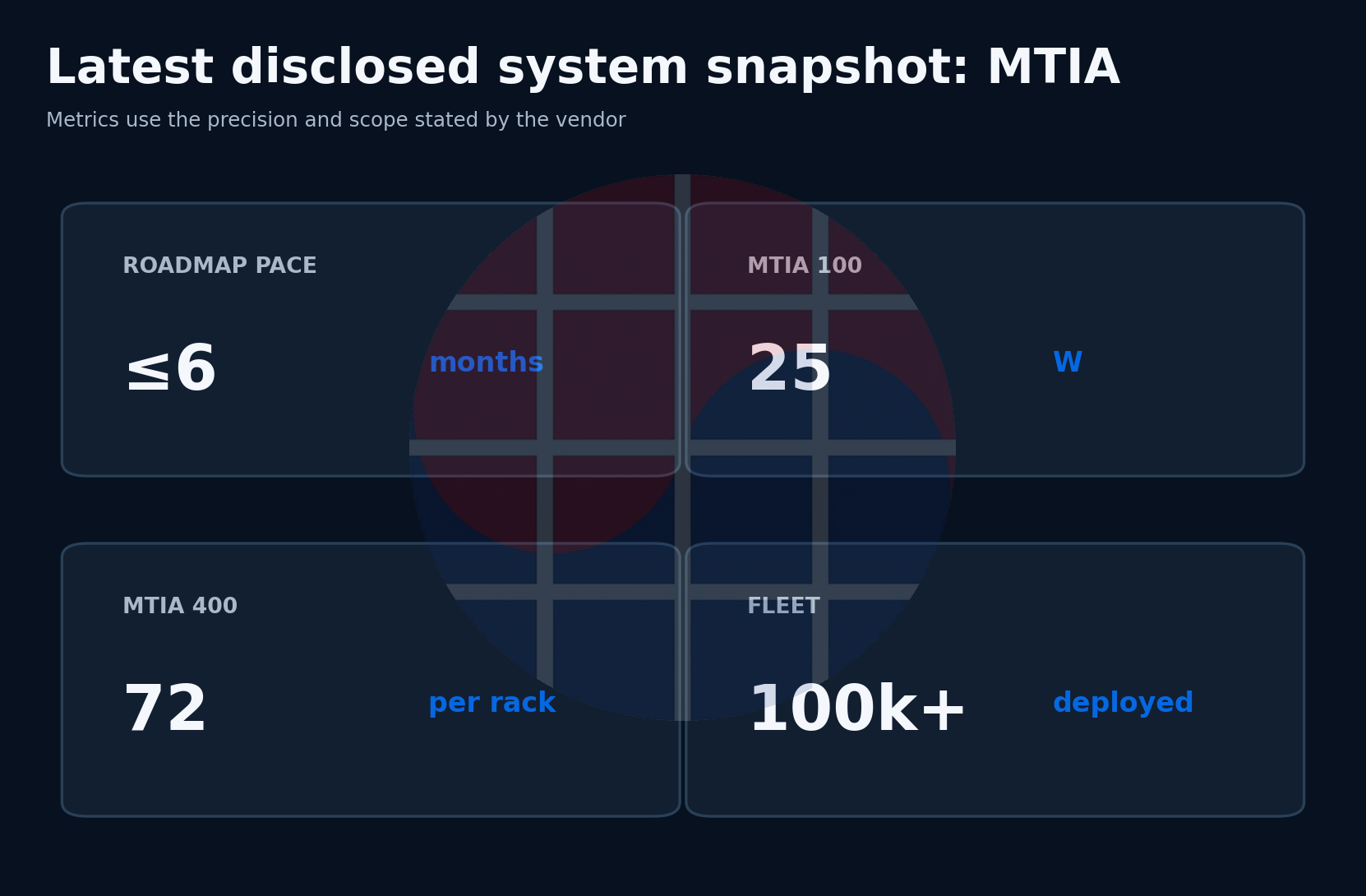
MTIA did not begin as a frontier-training GPU replacement. MTIA 100 used 25 W, LPDDR5, 128 MB of SRAM and 64 RISC-V processing elements to remove waste from small-batch ranking and recommendation inference. MTIA 200 moved to 5 nm, 90 W, 256 MB of SRAM and 128 GB of LPDDR5, then reached 16 regions quickly. MTIA 300 crossed into recommendation training with HBM, network chiplets and collective offload. MTIA 400 adds a 72-device scale-up domain and broader GenAI support; 450 and 500 emphasize HBM bandwidth, MX4 and GenAI inference.
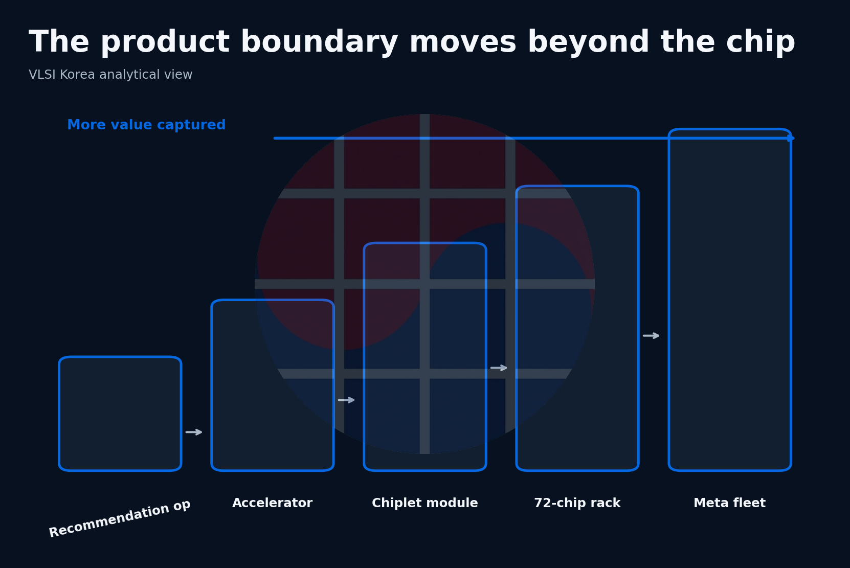
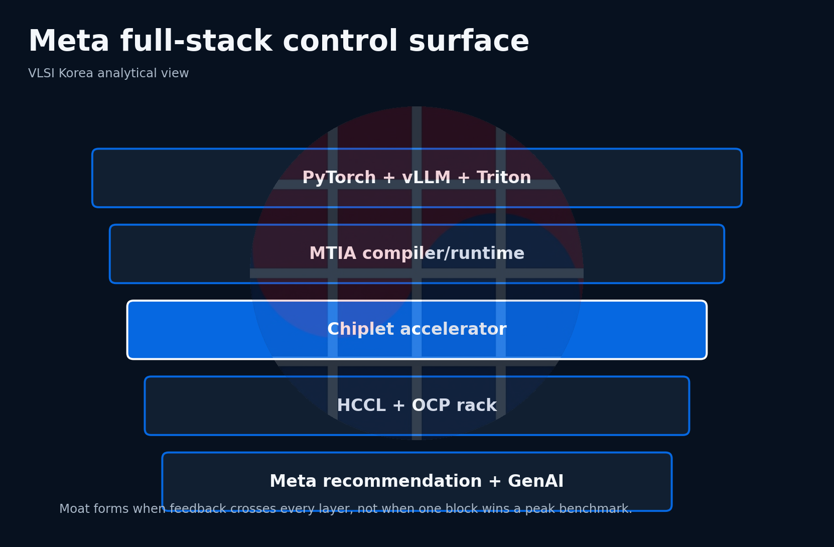
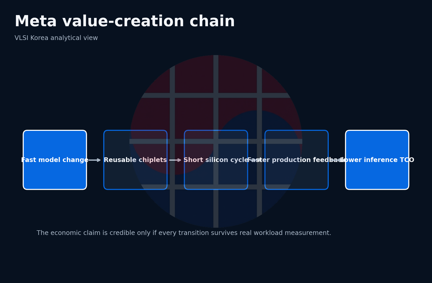
Meta can target an approximately six-month design cadence because compute, network and SoC chiplets, chassis, rack and software are reused. Its moat is control of PyTorch, Triton and vLLM plus the recommendation, advertising and GenAI traffic of billions of users. Its weakness is a lack of external market validation and the possibility that an inference-first design underperforms a flexible GPU on frontier training or irregular new models.
Generation map
| Generation | Workload focus | Memory direction | Compute and system direction | Deployment status |
|---|---|---|---|---|
| MTIA 100 | Ranking and recommendation inference | 64 GB LPDDR5, 128 MB SRAM | 25 W, 8 x 8 PE grid | Production foundation |
| MTIA 200 | Ranking and recommendation inference | 128 GB LPDDR5, 256 MB SRAM | 90 W, 3.5x dense compute | Large-scale production |
| MTIA 300 | Ranking and recommendation training | HBM-based chiplet system | Compute plus dual network chiplets | In production |
| MTIA 400 | R&R plus general GenAI | 51% more HBM bandwidth than 300 | 5x FP8, 72-device scale-up | Lab testing completed |
| MTIA 450 | GenAI inference | 2x HBM bandwidth vs 400 | 75% more MX4, attention and FFN acceleration | Mass deployment planned for early 2027 |
| MTIA 500 | GenAI inference | 50% more bandwidth and up to 80% more capacity vs 450 | 43% more MX4, 2 x 2 compute chiplets | Mass deployment planned for 2027 |
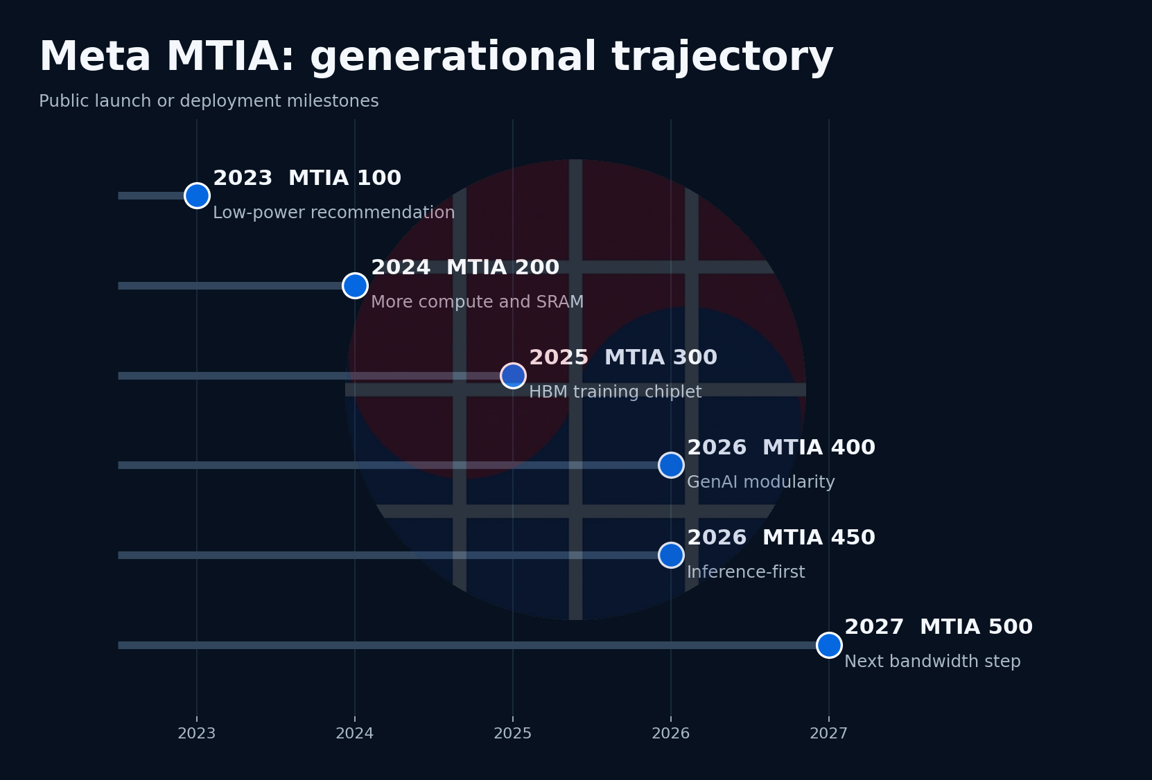
For MTIA 300 onward, Meta publishes many absolute specifications in images but not all in article text. The table uses the relative changes and deployment status explicitly stated in official prose.
Why recommendation is a rational ASIC starting point
Feed and advertising ranking run continuously at enormous volume, and Meta controls the model. The workload mixes embedding lookup, sparse access, feature interaction, small tensors and strict latency. Increasing batch size may improve GPU throughput while harming user-facing latency, leaving threads and HBM underutilized.
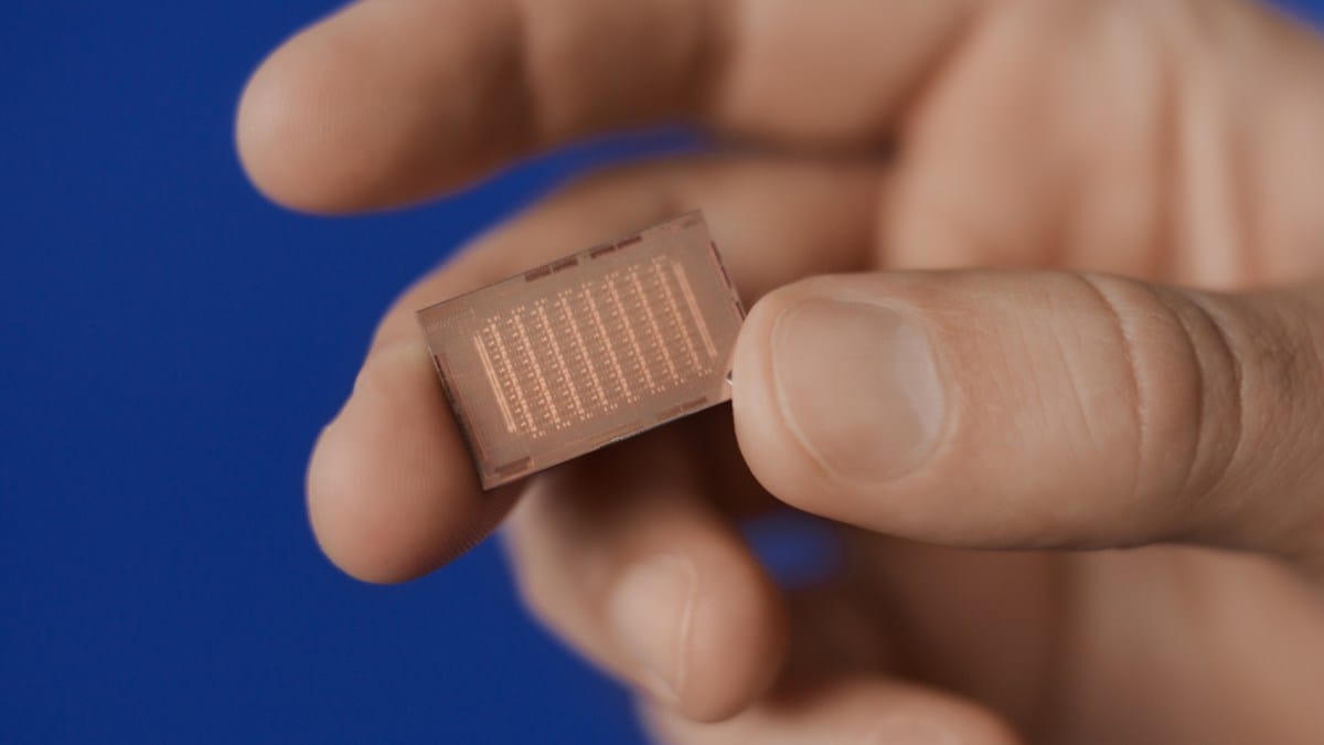
A tailored ASIC can pair large LPDDR capacity with unusually large on-chip SRAM, divide a processing grid into smaller subgrids, and adjust the balance of fixed-function blocks and programmable RISC-V cores. Meta still uses GPUs. The custom chip moves stable, high-volume work to lower TCO and preserves flexible GPUs for frontier and rapidly changing workloads.
MTIA 100: 25 W for small batches
Designed in 2020, MTIA 100 used TSMC 7 nm, an 800 MHz clock and a 25 W TDP. Peak compute was 102.4 INT8 TOPS or 51.2 FP16/BF16 TFLOPS. An 8 by 8 mesh joined 64 processing elements, each with two customized RISC-V cores, matrix, accumulation, nonlinear and data-movement units, and 128 KB of local SRAM.
The chip had 128 MB of shared SRAM and an LPDDR5 subsystem capable of as much as 128 GB; Meta's later comparison lists a 64 GB, 176 GB/s production configuration. Large SRAM kept hot data on chip when small batches offered little reuse. The 176 GB/s external bandwidth was insufficient for large dense models, and Meta reported weaker results on high-complexity workloads.
Twelve low-power accelerators fit in an air-cooled Yosemite V3 server. PyTorch FX IR, LLVM, eager and graph modes, C++ kernels and the KNYFE DSL formed the stack. Meta openly identified software optimization as a limitation, making operator coverage the real first-generation investment.
MTIA 200: more compute, the same SRAM thesis
MTIA 200 moved to 5 nm, 1.35 GHz, 421 mm² and 90 W. The 8 by 8 grid remained, while dense compute rose 3.5 times and sparse compute seven times. Dense peaks reached 354 INT8 TOPS and 177 FP16/BF16 TFLOPS.
Local SRAM per PE tripled to 384 KB, shared SRAM doubled to 256 MB and on-chip bandwidth rose from 800 GB/s to 2.7 TB/s. LPDDR5 provided 128 GB at 204.8 GB/s. Since off-chip bandwidth increased far more slowly than compute, Meta relied on SRAM reuse. A 72-accelerator rack and optional RDMA scale-out raised platform throughput.
The device reached production models in less than nine months and 16 regions because interfaces and software from MTIA 100 were retained. Triton-MTIA, TorchDynamo and TorchInductor let developers share front-end code with GPU deployments while keeping hardware-specific tuning in the backend.
MTIA 300: HBM and chiplets bring training
MTIA 300 combines one compute chiplet, two network chiplets and multiple HBM stacks. The compute PE includes two RISC-V vector cores, a dot-product engine, special-function and reduction engines, and DMA. Redundant PEs improve yield.
The network chiplets integrate NIC functions, message engines for collective offload and near-memory reduction. Recommendation training creates embedding, gradient and all-to-all traffic; moving those operations off the host and overlapping them with compute became the foundation for later GenAI systems.
Meta first deployed MTIA 300 for recommendation training, not frontier dense pretraining. It extended an inference program into the workload it understood best, using that controlled environment to learn failure recovery and software coverage before tackling more general GenAI.
MTIA 400, 450 and 500: bandwidth catches the GenAI workload
MTIA 400 increases FP8 peak five times over MTIA 300 while raising HBM bandwidth 51%. Two compute chiplets and enhanced MX8/MX4 increase density, and 72 devices form a switched scale-up domain. Compute grows much faster than bandwidth, which benefits dense GEMM but can strand decode performance. That imbalance explains the immediate 450 emphasis on memory.
MTIA 450 doubles HBM bandwidth over 400 and raises MX4 FLOPS 75%, adding hardware for attention, feed-forward networks, Softmax and FlashAttention. This combination targets MoE inference: MX4 reduces weight bytes, HBM feeds active experts and KV cache, and network chiplets dispatch tokens.
MTIA 500 adds another 50% of bandwidth, up to 80% more capacity and 43% more MX4 compute. Four smaller compute chiplets in a 2 by 2 arrangement sit beside HBM, two network chiplets and a SoC chiplet for host PCIe and scale-out. Repeating smaller dice improves yield and lets Meta replace only the block required by the next workload.
The 400, 450 and 500 generations share chassis, rack and network infrastructure. Reusable physical interfaces turn silicon cadence into deployment cadence. Meta's quoted 25-fold increase from MTIA 300 MX8 to MTIA 500 MX4 crosses numerical formats and must not be read as an equivalent quality-adjusted speedup.
Software and fleet moat
MTIA connects PyTorch eager and graph execution, torch.compile and torch.export, TorchInductor, Triton, MLIR and LLVM. A vLLM plugin replaces critical operations such as FlashAttention and fused LayerNorm while reusing prefill-decode disaggregation and continuous batching.
The Hoot Collective Communications Library drives message engines and near-memory reductions in the network chiplets. Collective fusion reduces launch and synchronization overhead. Fleet-wide telemetry and PE-level debugging matter because hundreds of thousands of chips turn intermittent hardware and firmware failures into daily operating events.
Watch points
- Whether MTIA 400 lab results survive production models and 72-device scale-up.
- Absolute HBM, process, power and package-yield data for 450 and 500.
- The range of Llama and advertising models that retain quality under MX4.
- Whether recommendation-training experience extends to general GenAI training.
- Whether a six-month design cadence can also be sustained in software qualification and mass deployment.
Contrarian read
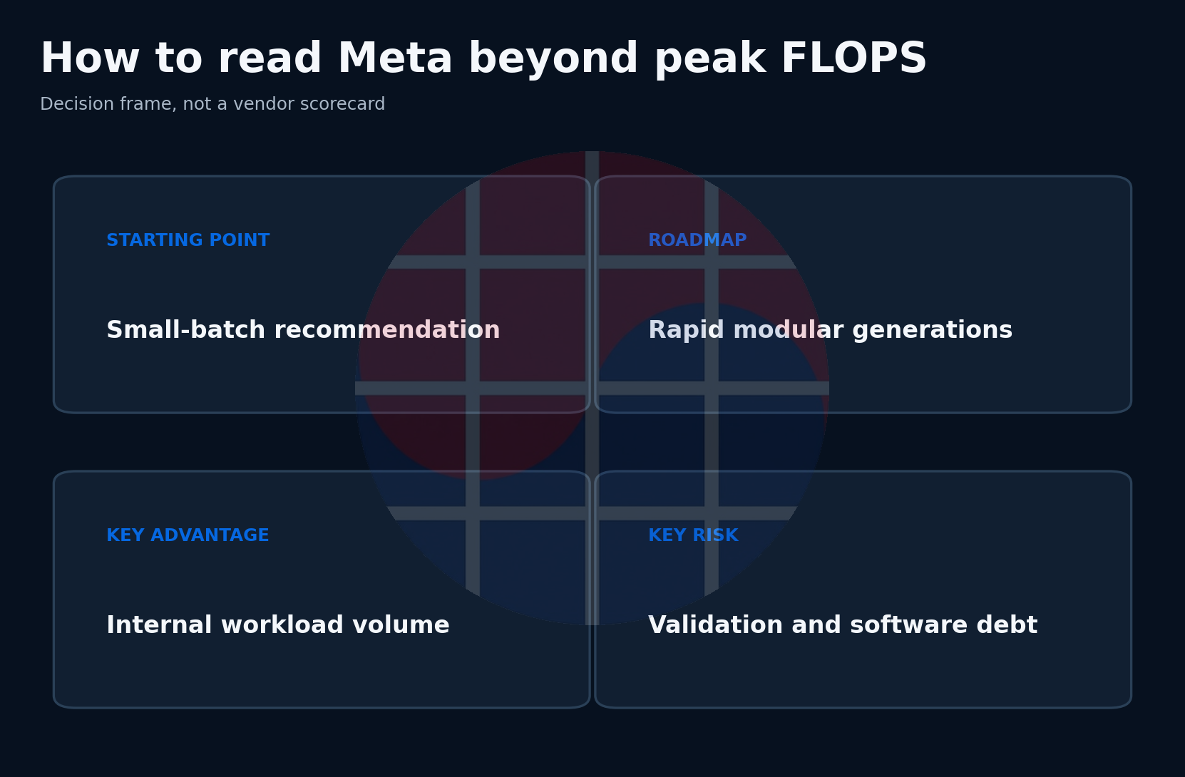
Chiplets and reusable racks shorten physical design, not model validation, compiler regression and fleet qualification. Rapid generations can force software teams to support several devices while revalidating production traffic. HBM and advanced-package supply may also lag the design cadence.
An inference-first device can be efficient on known Llama and recommendation graphs but lose to GPU SIMT flexibility when state-space models, multimodal encoders or agent runtimes create irregular control and memory behavior. Generation velocity can become the speed at which a wrong workload forecast is repeated.
Korean lens
MTIA shows that chiplets are an organizational cadence tool, not merely a die-partitioning technique. Stable compute, network, SoC, chassis and rack interfaces let only selected blocks change. A Korean chiplet strategy should therefore define independent validation and multi-generation reuse, not stop at UCIe compatibility.
The recommendation starting point is also practical for Korean internet and telecom operators. Search, advertising, speech, moderation and recommendation can finance a production software stack before a frontier-training chip. Companies that do not control PyTorch, the model and the datacenter as Meta does need even stronger partner and standards ecosystems.
Sources
- MTIA v1 architecture
- Next-generation MTIA
- Meta infrastructure overview
- Four MTIA chips in two years
- Meta infrastructure evolution
Disclosure
This article is for informational purposes only and does not constitute a recommendation to buy or sell any security. Figures and facts are based on publicly available corporate disclosures, media reports and market research, and errors may occur in the source material or writing process. The author may hold shares of companies mentioned. Readers are solely responsible for all investment decisions and outcomes.