VLSI Korea
ABF Substrates, Dissected — The Physics, the Double Monopoly, and the .8B Bet Beneath Every AI Chip
A full dissection of the substrate beneath every AI chip: Ajinomoto's 95% film monopoly, the SAP process and yield arithmetic, warpage physics, the T-glass double bottleneck, 2027-28 gap forecasts, and why glass will not kill ABF.


🆓 Free article · Anyone can read this article for free
The 30-Second Summary
- The conclusion first: what now decides whether an AI accelerator ships is not the GPU die or the HBM. It is the substrate underneath — and the insulating film inside that substrate comes, more than 95% of it, from a Japanese seasoning company, Ajinomoto.
- On October 21, 2026, Samsung Electro-Mechanics (SEMCO) and NVIDIA officially announced a strategic partnership to co-invest in dedicated FC-BGA lines at SEMCO's Sejong and Busan plants. Reuters reported the next day that NVIDIA (about ₩2.6 trillion) and Tesla (about ₩1.1 trillion) are putting a combined ₩3.7 trillion ($2.8B) behind SEMCO's expansion. Chip companies now fund substrate factories.
- The demand math is brutal. A large AI substrate has roughly 3.5x the area and 3x the ABF layers of a conventional one — about 10x the film consumption (Ajinomoto's 2025 integrated report). By Ibiden's measure, the process load of one AI substrate rises to 1.8x its 2024 level in 2026 and 2.5x in 2028.
- Supply-gap forecasts differ by institution but agree on direction. Morgan Stanley sees supply falling 9.3% short of demand in 2027 and 13.7% in 2028, with price increases above 25% in 2027. BofA is darker: gaps of 7%, 14% and 19% across 2026-2028.
- Glass substrates will not kill ABF. Glass replaces only the substrate's core; the build-up layers on top are still ABF film. Ajinomoto's chokehold survives into the 2030s.
This is the technical companion to our October 17 analysis, "ABF Substrate Supply Crunch", which followed the money — capacity races and margins. This piece dissects the substrate itself: the chemistry of the film, the physics of the process, the arithmetic of yield, and the structure of a double monopoly.
Prologue: Why Chip Companies Are Funding a Substrate Factory With $2.8 Billion
On October 21, 2026, at GTC in Berlin, SEMCO and NVIDIA made their partnership official (SEMCO announcement; TheElec). Three elements matter. First, the two companies will co-invest to build dedicated AI package-substrate (FC-BGA) capacity at SEMCO's Sejong and Busan sites in Korea. Second, SEMCO will supply substrates for NVIDIA's AI compute chipsets and data-center networking switches for multiple years starting in 2026. Third, volumes grow at a double-digit annual rate, and by 2028 NVIDIA is expected to account for a significant share of SEMCO's entire package-substrate capacity.
Attached to the deal is a technical detail that is easy to miss: MLCCs and silicon capacitors embedded inside the substrate. The point is to kill power noise directly beneath the die — a combination only SEMCO can offer, because it is simultaneously the world's leading MLCC maker and a top-tier FC-BGA producer. SEMCO CEO Chang Duck-hyun framed it as combining "advanced FC-BGA manufacturing competitiveness with unmatched high-reliability MLCC technology." NVIDIA's EVP of Operations, Debora Shoquist, said the work "broadens our network of substrate partners and adds manufacturing capacity."
The next day, Reuters — citing a Maeil Business Newspaper report — filled in the money. Customer funding of about ₩3.7 trillion ($2.8B) supports SEMCO's Sejong expansion: roughly ₩2.6 trillion from NVIDIA and ₩1.1 trillion from Tesla. Tesla's structure, as reported, is a dedicated line at Sejong supplying substrates for its autonomous-driving and Optimus humanoid-robot AI chips for five years, 2029-2033. In other words, customers are funding a large slice of the ₩4.27 trillion Sejong portion of the ₩6.78 trillion program SEMCO announced on September 28 (the other ₩2.51 trillion goes to Hai Phong, Vietnam). SEMCO's disclosed long-term agreements since May now total seven contracts worth a cumulative ₩4.3 trillion.
Why does this happen? Because FC-BGA lead times have stretched from a normal ~12 weeks to 48-56 weeks (Hana Securities estimate), SEMCO's substrate utilization ran at 89% in the first half of 2026 (LG Innotek reportedly 94%), and a server FC-BGA is more than 4x the area and more than 2x the layer count of a PC one — buildable by only a handful of companies on Earth. This is a market where customers co-fund factories to reserve capacity. To understand why, you have to understand what a substrate actually does.
Chapter 1. The Substrate Is a Motherboard Inside the Package
A semiconductor die cannot talk to the world on its own. Connection pads on the die are spaced tens of micrometers apart; traces on a motherboard are spaced hundreds of micrometers to millimeters. The package substrate is the translator across that near three-orders-of-magnitude gap. It does four jobs.
First, fan-out. It spreads tens of thousands of die connections outward to a pitch the board can accept. In AI accelerator packages, the signal count a substrate routes has moved from thousands into the tens of thousands.
Second, power delivery. A modern accelerator draws over 1,000W at around one volt — currents on the order of 1,000 amps. At that point the resistance and inductance of the delivery path are performance. That is why SEMCO embeds MLCCs and silicon capacitors inside the substrate: moving the decoupling capacitor from millimeters away to hundreds of micrometers beneath the die cuts power noise where it is born.
Third, signal integrity. NVLink and SerDes lanes cross the substrate at tens to hundreds of gigabits per second. The dielectric constant (Dk) and loss tangent (Df) of the insulating material set loss and distortion. ABF became the high-end standard partly for its low dielectric loss and its smooth surface, which improves copper adhesion and reduces skin-effect losses.
Fourth, mechanical support and the thermal path. Reflow soldering runs to about 250°C. Through that cycle, the substrate must hold the package flat enough that tens of thousands of bump connections survive. As Chapter 5 shows, it is this fourth job that is hitting its physical limit first.
Call it what it is: the substrate is a second motherboard, shrunk inside the package. As chips grow larger, faster and hotter, the difficulty of that inner motherboard is catching up with the chip itself.
Chapter 2. What ABF Actually Is: A Seasoning Company's Secret Sauce
1996: Intel's Request. 1999: Mass Production.
ABF (Ajinomoto Build-up Film) is the interlayer insulating film made by Ajinomoto Fine-Techno, a subsidiary of Ajinomoto — the company that commercialized MSG. The origin is a 1996 commission from Intel, which needed a film-type insulator for next-generation CPU substrates. The incumbent approach — coating liquid resin and drying it, one side at a time — struggled with thickness uniformity and particle contamination. Ajinomoto's researchers (Shigeo Nakamura, now the company's president, was on the team) turned the material into a film, and mass production began in 1999 for the Pentium III. Vacuum-laminating film onto both sides of a panel at once simplified the process, and shipping the varnish coated on film — in frozen form — was a manufacturing idea the semiconductor industry had not imagined, and a food company had.
That a company built on amino-acid chemistry ended up atop a semiconductor material is not an accident. ABF's core is a formulation: more than ten raw materials — epoxy resin, hardeners, inorganic filler particles — blended and dispersed uniformly. Internally it is called the "secret sauce." Organic and inorganic materials do not naturally mix; dispersing them uniformly while hitting dielectric, thermal-expansion, laser-drilling and copper-adhesion targets simultaneously is the accumulated craft. The formulation is the performance.
ABF by the Numbers
| Property | Representative level | Why it matters |
|---|---|---|
| Market share | Over 95% (company figure) | Effectively a single source for CPU/GPU-grade build-up film |
| Dielectric constant (Dk) | ~3.2-3.5 | Lower Dk means less delay and loss for high-speed signals |
| Fine-line capability | Line/space down to ~5 µm (SAP) | Subtractive limit 75 µm → SAP 15 µm → ~5 µm class today |
| Grade families | GL (low loss), GX (standard), GZ (low CTE), and others | Customer-specific grades deepen the lock-in |
| Form factor | Rolls of film | Laminated by substrate makers into build-up layers |
Note the grade strategy. Ajinomoto co-develops grades tuned to each customer's process. For a substrate maker, switching film means re-tuning lamination, laser, plating and inspection — and then re-qualifying with the end customer, a process that takes 18-24 months. The deepest moat is not the recipe; it is that nobody can afford to switch. Sekisui Chemical is the only other supplier with a mass-produced, SAP-compatible build-up film, and its share sits in the low single digits.
Transistors have shrunk by orders of magnitude in 27 years. The film beneath them has had one supplier the entire time.
Chapter 3. How an FC-BGA Is Made: An Eight-Step Cycle, Repeated
An ABF substrate is not built in one process. It is built in a cycle, repeated once per layer. At the center sits a rigid core — glass-cloth fabric impregnated with resin, clad in copper. Build-up layers are stacked on both faces. Learn the notation: "10-X-10" means ten build-up layers on each side of the core, roughly twenty layers in total. On Ibiden's roadmap, AI-server substrates move from 10-X-10 in 2026 to 12-X-12 in 2028 and 14-X-14 from 2030.
- Core fabrication: holes are drilled and plated through the copper-clad laminate to form the core wiring. The core's stiffness and thermal expansion govern the warpage of everything above it.
- Lamination: ABF film is vacuum-laminated onto the surface. A single trapped bubble is a defect.
- Curing: heat hardens the film into an insulating layer.
- Laser vias: CO₂ or UV lasers drill microvias tens of micrometers wide — the vertical paths between layers.
- Desmear: resin residue charred by the laser is chemically removed. Fail here and the plating will not stick.
- Seed plating: electroless copper lays down a thin seed layer.
- SAP patterning: photolithography defines the circuit; electrolytic plating grows copper only where it is needed — the semi-additive process that ABF's smooth surface made practical, and the source of its fine-line advantage.
- Inspect, then repeat: only panels passing electrical and optical inspection go up a layer. Then back to step two. Per layer.
This cycle structure makes yield arithmetic cruel. At 99% yield per layer, a 24-layer substrate finishes at 0.99^24 — about 79%. At 97% per layer, about 48%. One failed layer scraps the entire panel, including every hour of equipment time already spent on it. That is why "nameplate capacity" and "effective capacity" are different numbers, and why the gap between them widens as layer counts rise.
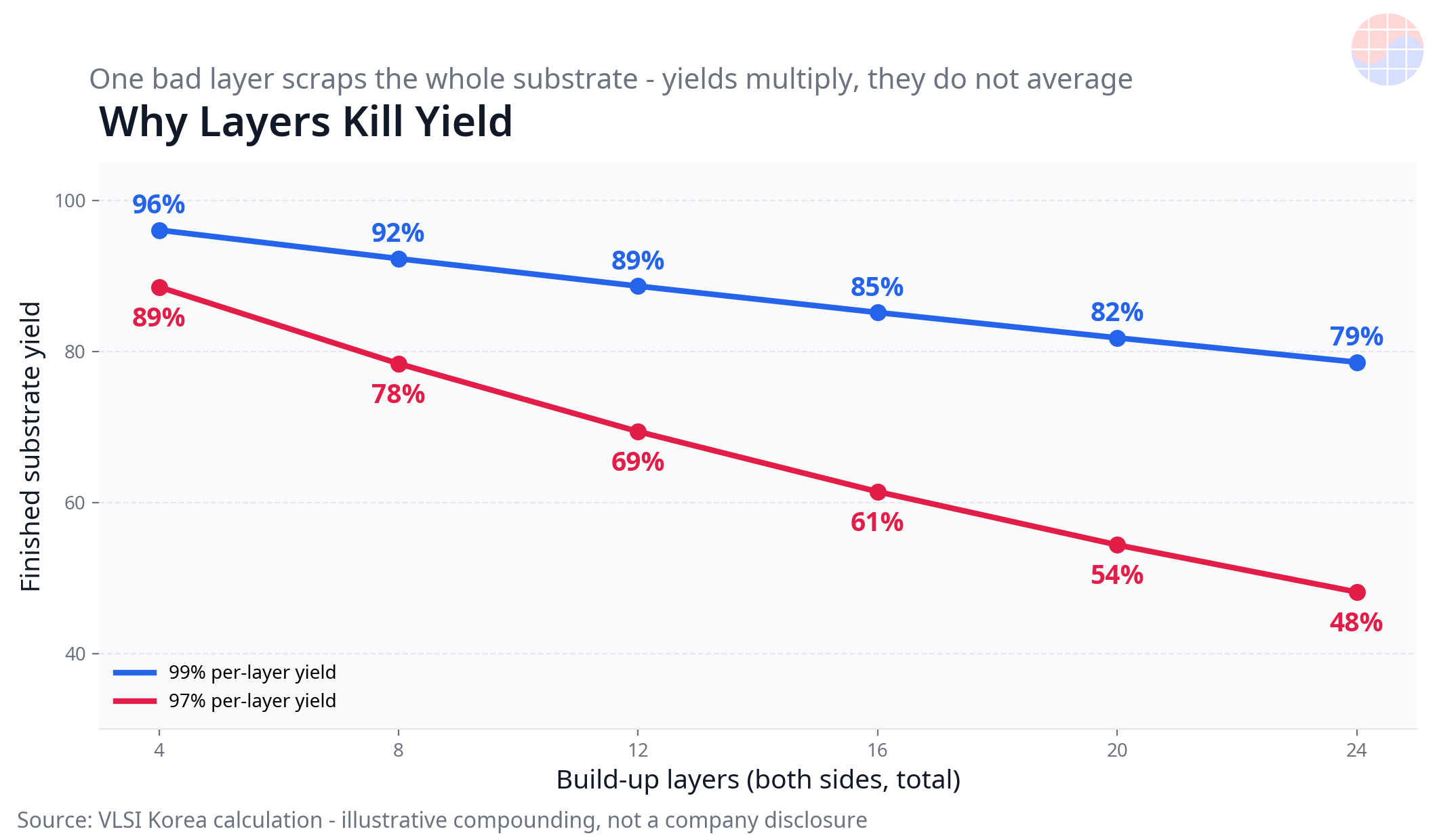
It is also why capacity announcements must be discounted three times: for equipment delivery, for yield ramp, and for customer qualification. At the TPCA show on October 20, 2026, Unimicron's chairman put numbers on the first of those: lead times for key equipment now run to 30 months, with more than 80% of equipment delayed. Factories are slow; equipment is slower; yields are slower still; qualification is slowest.
Chapter 4. The Demand Math: Area × Layers = 10x the Film
ABF demand cannot be counted in chip units. The film consumed per substrate is exploding. Ajinomoto's 2025 integrated report gives the cleanest decomposition: a large AI substrate has about 3.5x the board area and about 3x the ABF layers of a conventional design — roughly 10x the ABF consumption.
Area growth is forced by the packaging roadmap. TSMC's CoWoS scales from about 3.3 reticle sizes in current volume production to 5.5 in 2026, 9.5 in 2027 and beyond 14 by 2029. Ibiden's substrate-size roadmap runs from 90×90 mm in 2026 to 110×110 mm in 2028 and 130×130 mm or larger from 2030. Industry estimates put NVIDIA's Rubin-generation substrate about 40% larger than Blackwell's, with layers rising from 14 to 18, and Rubin Ultra substrate ASPs rising at least another 50% over Rubin.
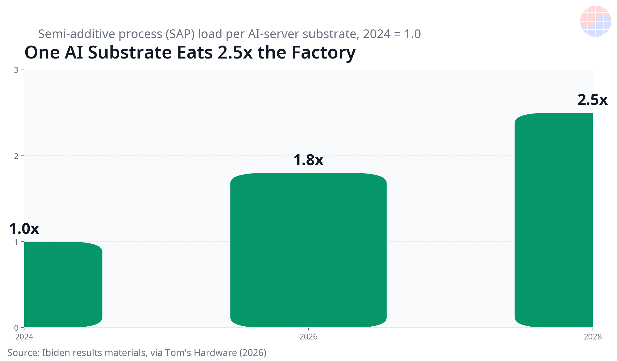
This is why Ibiden measures demand not in substrates but in SAP process load. If one substrate occupies factory equipment 1.8x as long in 2026 and 2.5x as long in 2028 as in 2024, doubling the factory still leaves the market tighter. Supply-chain analyses that put substrate-area demand growth near 39% CAGR for 2025-2028 are measuring the same thing: the real unit of demand is area × layers × process time, not units.
And the buyer list is widening. Beyond GPUs and custom ASICs (Google TPU, AWS Trainium and peers), server CPUs are becoming a bottleneck of the agent era — and now Tesla's driving and robotics chips have joined the FC-BGA queue. Tesla appearing as a funder of SEMCO's dedicated line is symbolic: the substrate contest is escaping the data center.
Chapter 5. The Physics Wall: Warpage
As substrates grow, the first limit encountered is not equipment or money. It is thermal expansion. A package is bonded in a reflow process at about 250°C and then cools. Its materials contract at wildly different rates: silicon at about 2.6 ppm/°C, copper at 17, organic cores at 14-17, and ABF film on its own is cited up to around 30. Materials shrinking at different speeds inside one bonded package pull against each other — and the substrate bows.
📩 Following this story?
Get the follow-up analysis — earnings, reports and HBM supply — in your inbox daily at 10:30 KST. Subscribe free →
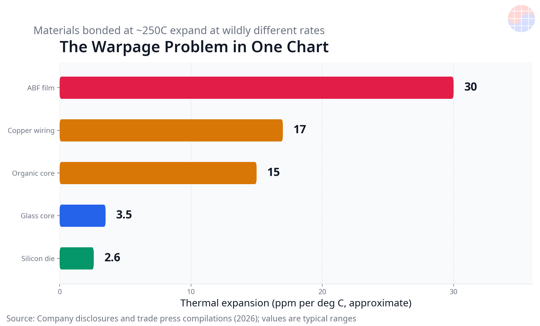
Warpage is fatal because the precision budget is microscopic. CoWoS micro-bump pitches run at 40-55 µm, and joints form only if flatness holds within tens of micrometers across the whole package. The working rule in the industry is that organic substrates struggle to hold usable flatness beyond roughly 120 mm per side. Ibiden's 2030 roadmap target of 130×130 mm sits exactly beyond that wall.
The case study already happened. Trade reports say NVIDIA's original quad-die Rubin Ultra configuration was redesigned after organic-substrate warpage made the economics fail. At the same time, reports indicate the alternative — CoWoP, which deletes the substrate entirely by mounting the package wafer directly on the PCB — was not adopted for Rubin Ultra, which stays with ABF substrates, because of yield and supply-chain reorganization risk. Even NVIDIA is fighting the substrate's physics from both directions: it cannot yet live with a much bigger one, and it cannot yet live without one.
Chapter 6. The Double Monopoly: Inside the Film, Another Monopoly
Peel the ABF supply chain one layer deeper and there is a monopoly inside the monopoly. The low-CTE glass cloth that reinforces substrate cores — T-glass, the material that keeps large packages dimensionally stable — comes about 90% from one Japanese supplier, Nittobo. E-glass substitutes cannot meet AI-grade specifications. In 2026, T-glass prices rose 20-30%, copper-clad laminate lead times stretched from a normal 8-10 weeks to beyond 20, and some buyers report that suppliers stopped quoting lead times at all. Nittobo is tripling capacity at its Fukushima plant, but new supply does not reach the market before mid-2027 at the earliest. Specialty glass — melted in electric furnaces at 1,600-1,700°C, spun and woven ultrathin — has no on/off switch.
So every AI package stands on two Japanese single sources stacked in series: Ajinomoto with over 95% of build-up film, Nittobo with about 90% of low-CTE glass cloth. A substrate maker can build all the factories it wants; if either material stops, the line stops. Ajinomoto's notice in May 2026 of a ~30% ABF film price increase effective Q3, alongside reported cuts to film shipments to China, is what this structure looks like when exercised. The direct pass-through of a 30% film increase to finished substrate prices is estimated at only 3-6% (Commercial Times) — the real effect is the second round, substrate makers' own increases: ABF substrate prices at Kinsus rose about 5% in H1 2026 with up to 7% more expected in H2, and GPU substrate ASPs are estimated to have risen from $65 in 2024 to $82 in 2025.
Ajinomoto's own response speed tells the same structural story. Film capacity ran at full load at a reported two million square meters per month in Q2 2026; a new Gunma plant entered full operation in 2025. The company has invested roughly ¥25 billion since 2023 and plans at least as much again by 2030, targeting over 50% more capacity. But its third varnish production base only signed its land deal in May 2026, with construction planned for 2028 and operations in 2032. For one of the world's most consequential semiconductor materials, the supply curve bends six years out. Challengers exist — US startup Thintronics signed a letter of intent in July 2026 for up to $50 million in CHIPS R&D incentives, and Chinese films such as Huazheng's CBF are in qualification — but the 18-24-month qualification wall makes them late-decade variables, not present answers.
Chapter 7. The Gap Forecasts: Different Numbers, Same Direction
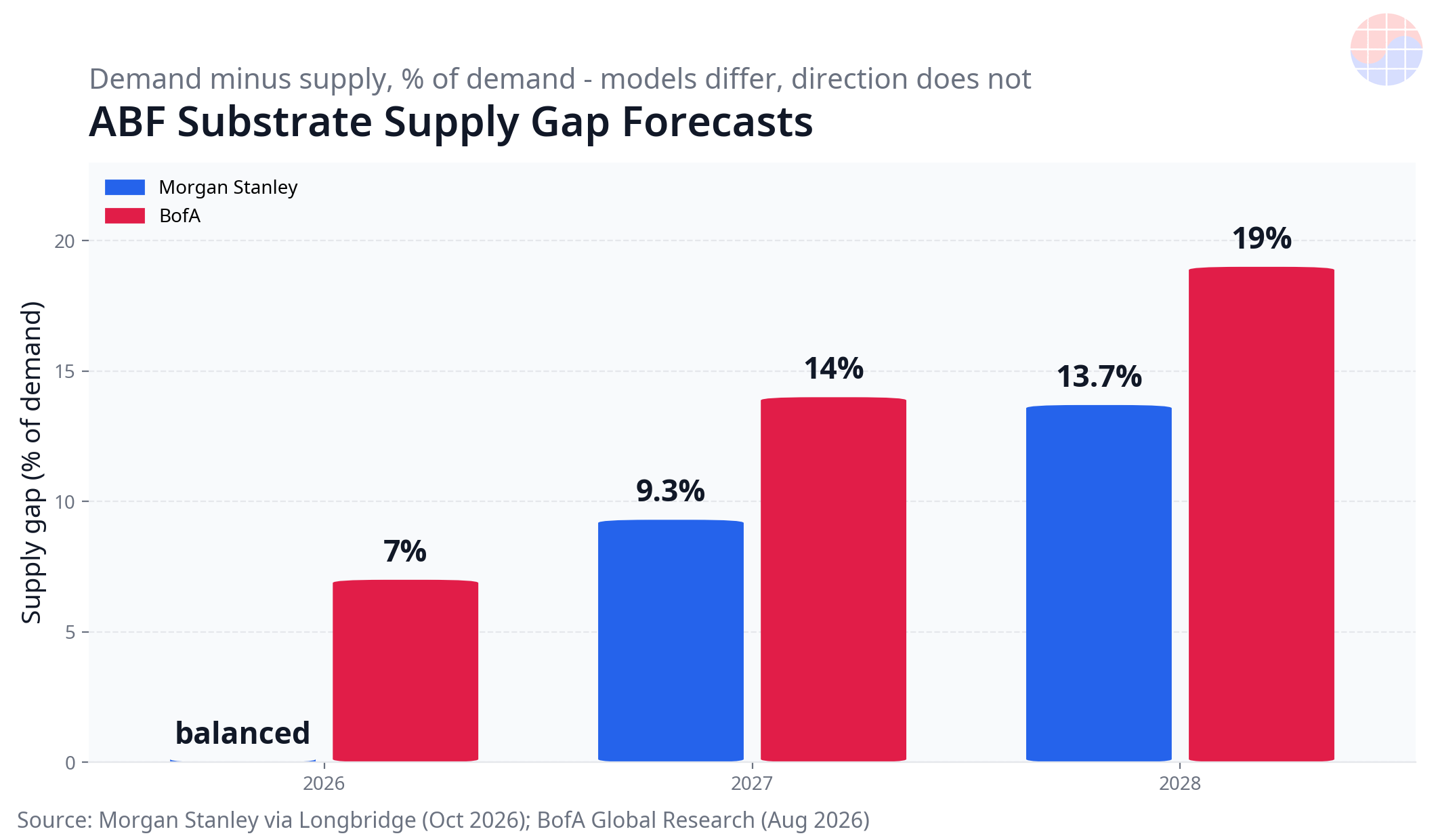
Morgan Stanley's latest supply-demand model has 2026 roughly balanced, then a 9.3% shortfall in 2027 and 13.7% in 2028 — revised up from 6.2% and 9.4%. On price, it expects 2027 increases to exceed 25%, and draws a distinction: 2026 increases were raw-material pass-through, while 2027's will be made by the supply-demand balance itself. BofA is more bearish: shortfalls of 7% in 2026, 14% in 2027 and 19% in 2028, citing the gross-margin improvement at all three Taiwanese substrate makers in Q2 2026 as the first hard evidence of a seller's market. Some supply-chain analyses leave 2028 open as far as 40%.
The forecasts diverge because the denominator differs. Divide by nameplate capacity and the gap looks small; divide by effective capacity — derated for area, layers and SAP load — and it doubles. The common ground is threefold: most new capacity reaches volume in H2 2028 through 2030; until then the demand slope (area × layers) outruns the supply slope; and pricing power sits with suppliers. Unimicron's chairman compressed it into one comparison at TPCA: against 2024, CoWoS capacity grows 6.8x and hyperscaler capex 6.3x by 2028, while IC substrate capacity merely doubles and DRAM capacity grows 1.8x. The front and back of the packaging flow are scaling sixfold; the substrate between them, twofold.
These are models, not measurements. As our earlier fact-check of semiconductor price forecasts showed, point estimates should be read as direction plus conditions. For ABF the conditions are explicit: the gap narrows only if announced expansions ramp on schedule, new lines yield quickly, and package area/layer growth slows. Miss any one of the three and the error lands on the wider side.
Chapter 8. The Substrate Oligopoly — and Korea's Seat at the Table
If film is a monopoly, substrate manufacturing is an oligopoly. High-end FC-BGA share is estimated at roughly 35% for Ibiden, 18% for Shinko and 14% for Unimicron, with AT&S, Nan Ya PCB, Kinsus, SEMCO and LG Innotek behind them. The moat is not the factory shell; it is accumulated yield and qualification. Making a 20-plus-layer, large-format substrate that passes NVIDIA, AMD or Google qualification takes three to four years of process learning that money alone cannot compress.
Korea holds two cards. The first is SEMCO's "substrate-plus" fusion: it is the only major substrate maker that also manufactures MLCCs at scale, and embedding those capacitors — plus silicon capacitors — inside the substrate became the technical rationale for the NVIDIA deal. Customer funding of ₩3.7 trillion against a ₩6.78 trillion program is something the substrate industry has not seen before. SEMCO's package-solutions division reportedly posted H1 2026 sales of ₩1.497 trillion (+41% year on year) and operating profit of ₩160.2 billion (+237%). The second card is LG Innotek's Hai Phong, Vietnam base, expanding FC-BGA capacity from a reported 94% utilization — a play on cost and geographic diversification.
Korea's bottleneck is equally clear. Both single-source materials — Ajinomoto's film and Nittobo's T-glass — sit in Japan. SEMCO's glass-core joint venture with Sumitomo Chemical Group (next chapter) is, in effect, managing Japanese materials dependence through a Japanese partnership. Korean laminate and materials makers, Doosan Electro-Materials among them, qualifying T-glass alternatives and low-loss materials would be worth more than another factory: it would move the ceiling on Korean substrate margins, which today is set by someone else.
Chapter 9. Glass Substrates: Not Here to Kill ABF
The most common misconception about glass substrates is that glass replaces ABF. It does not. A glass substrate replaces the substrate's core. Swap the organic core for glass — whose thermal expansion can be tuned close to silicon, and which can carry through-glass vias — and you get a flatter platform for finer wiring and larger packages. But the build-up insulation stacked on both sides of that glass core is still ABF film. Glass is Ajinomoto's customer, not its assassin. If anything, packages beyond 130 mm consume more film, not less.
| Player | Roadmap (public information as of Oct 23, 2026) | Notes |
|---|---|---|
| SKC / Absolics | $600M Covington, Georgia plant; samples shipping from January 2026 | AMD evaluation reported; second-phase expansion reportedly under reconsideration |
| SEMCO (GlaSSEM) | Glass-core JV with Dongwoo Fine-Chem finalized July 2, 2026: ₩480B total, SEMCO 66.2%, full-scale operations targeted H2 2027 | Prototypes and customer evaluation running on the Sejong pilot line |
| Intel | EMIB + glass sample shown at NEPCON Japan, January 2026: 45 µm bump pitch, ~2x reticle class, "No SeWaRe" no-microcrack claim | Own deployment toward ~2030; reported shift toward licensing |
| TSMC | CoPoS 310×310 mm panel pilot in 2027, volume production targeted H2 2028 | Most analyses place glass-core commercialization after 2030 |
The timeline history teaches caution. Absolics originally targeted mass production in H1 2024; SEMCO's glass milestones have reportedly slipped on reliability. Glass's bottlenecks are not ideas but TGV drilling yield, handling breakage, and customer qualification — precisely the same three walls as ABF substrates. The realistic picture: organic cores plus better ABF (low-loss grades, low-CTE cores, warpage control) carry the late 2020s; glass cores enter from the largest packages around the turn of the decade; and ABF film rides on top throughout. Not the death of ABF — a replacement of the floor it stands on.
Chase's Take: The Power Is in the Film, and the Contracts Just Admitted It
First, the profit pool in this chain is asymmetric. Ajinomoto runs a capital-light materials monopoly and raises prices from a position of stillness (+30% in Q3 2026). Substrate makers pour trillions of won into factories and remain hostages to yield and qualification. Unimicron's gross margin doubling from 11.6% to 24.8% in 18 months is impressive — and it exists at the pleasure of the company that prices its film. When reading any supply chain, ask not "who has capacity" but "whose absence stops everything." In the ABF chain the answer has been one company for 27 years.
Second, the NVIDIA-Tesla co-investment is the HBM pattern replayed in substrates. HBM moved from purchase to pre-purchased capacity through long-term agreements and prepayments; substrates just made the same transition. Watch Tesla's presence: the moment demand widens from data-center GPUs to vehicles and robots — larger volumes, longer product lives — the substrate contest becomes structural, independent of any AI-bubble debate.
Third, Korea's winning move is fusion and materials, not capacity. SEMCO's embedded MLCC is the first proven "substrate-plus" case. By the same logic, a Korean qualification win in T-glass, low-loss materials or advanced laminates would build a longer moat than another fab. Leaving film and glass-cloth dependence untouched while adding factories means the margin ceiling keeps being set abroad.
Fourth, four checkpoints decide the next twelve months: Unimicron's Q3 results on October 27 (ABF margins and backlog commentary), the pace of SEMCO's LTA disclosures and Sejong schedule, Ajinomoto's second-round pricing and Gunma ramp, and T-glass supply when Nittobo's expansion lands in mid-2027.
Scenarios
- Base case: a high-single-digit to double-digit supply gap in 2027, double-digit substrate price increases, and supplier margin expansion lasting until the 2028 H2 capacity ramp.
- Bull case (for suppliers): Rubin Ultra-class area demand and CPO substrates overlap while T-glass binds first, pushing the gap past BofA's path (19% in 2028). Customer co-investment becomes the industry standard.
- Bear case: an AI capex correction turns pre-built capacity into a burden. Unlike HBM, though, substrate demand is diversified across CPUs, networking and automotive — a correction more likely slows price increases than repeats the 2021-2023 collapse.
FAQ
Q1. What is an ABF substrate? A high-performance package substrate built with Ajinomoto Build-up Film as its insulating layers. It connects GPUs, CPUs and AI accelerators to the motherboard, routing fine wiring and thousands to tens of thousands of signal and power paths. FC-BGA is the representative format.
Q2. Why is Ajinomoto a monopoly? It mass-produced the first film-type build-up insulator in 1999, built lock-in through a formulation of more than ten raw materials and customer-specific co-developed grades, and any switch requires 18-24 months of process re-tuning and customer re-qualification. Its share above 95% has held for 27 years.
Q3. When does the ABF shortage end? Institutional forecasts converge on shortfalls of 9-14% in 2027 and 14-19% in 2028. Most new capacity reaches volume between H2 2028 and 2030, so a tight market likely persists until then. Nittobo's T-glass expansion landing in mid-2027 is the first relief signal.
Q4. Will glass substrates make ABF obsolete? No. A glass substrate replaces only the core; the build-up insulation on top remains ABF film. Glass timelines also run from 2027 to beyond 2030, and larger packages increase film consumption rather than reducing it.
Q5. Why are NVIDIA and Tesla investing in Samsung Electro-Mechanics? Because FC-BGA lead times have stretched to 48-56 weeks and only a handful of suppliers can build AI-grade substrates. SEMCO and NVIDIA announced co-investment in dedicated lines and multi-year supply on October 21, 2026, and Reuters reported about ₩2.6 trillion from NVIDIA and ₩1.1 trillion from Tesla backing the Sejong expansion — capacity secured by building the factory together, not by bidding in the spot market.
Q6. What is T-glass and why is it a bottleneck? The low-thermal-expansion glass cloth inside substrate cores, critical to controlling warpage in large packages. Japan's Nittobo supplies about 90% of it, and its expansion does not arrive until mid-2027 — a second monopoly stacked under Ajinomoto's.
Q7. What should investors watch? Substrate makers' margin trajectory (ABF mix and price pass-through), customer LTA and co-investment disclosures, Ajinomoto and Nittobo pricing and expansion announcements, and yield commentary in quarterly results. Forecast numbers diverge by institution — read direction and conditions, not point estimates.
This analysis is based on company announcements and reporting available as of October 23, 2026, and is not investment advice. Institutional forecasts and industry estimates are attributed in the text; unverified figures are marked as estimates.
Sources
- SEMCO-NVIDIA strategic partnership (Oct 21, 2026): https://www.thelec.kr/news/articleView.html?idxno=64086
- Reuters — SEMCO to receive ₩3.7T investment from Tesla, NVIDIA (Oct 22, 2026): https://www.channelnewsasia.com/business/samsung-electro-mechanics-gets-28-billion-chip-investment-tesla-nvidia-report-says-6481841
- ChosunBiz — Big tech fund SEMCO's Korea substrate expansion (Oct 22, 2026): https://biz.chosun.com/en/en-it/2026/10/22/SG2GD2JAY5CRXBVX7U3I4N6VZ4/
- Morgan Stanley ABF supply-demand and pricing outlook (Oct 2026): https://longbridge.com/en/news/301862838
- Tom's Hardware deep dive — ABF substrates and the material wall (2026): https://news.lavx.hu/article/abf-substrates-in-data-center-silicon-solving-the-supply-crunch-beneath-every-ai-accelerator
- SEMCO-Sumitomo glass core JV (Jul 2, 2026): https://en.infomaxai.com/news/articleView.html?idxno=128368
📩 Missed today's analysis? Get tomorrow's in your inbox
Daily Silicon at 10:30 KST plus earnings and analyst-report breakdowns, first. Samsung Electronics, SK hynix, TSMC and HBM supply, read by practicing engineers. Join 300+ subscribers.
Subscribe free →
Free · No spam · Unsubscribe anytime