VLSI Korea
Advanced Packaging Passes Half the OSAT Market in 2026 — and Is Still 10–20% Short (CoWoS, HBM)
Advanced packaging passes 50% of the OSAT market in 2026, yet capacity runs 10-20% short of demand even as TSMC scales CoWoS to 120k-140k wafers per month. When packaging is the bottleneck, pricing power moves downstream.


30-Second Summary
- Advanced packaging is forecast to exceed 50% of the total OSAT market in 2026. The back end of chipmaking — assembly, stacking, and test — becomes the majority business of the outsourced packaging industry for the first time.
- It is still not enough. Industry capacity for advanced packaging is expected to run 10–20% short of demand in 2026, even after aggressive expansion across foundries and OSATs.
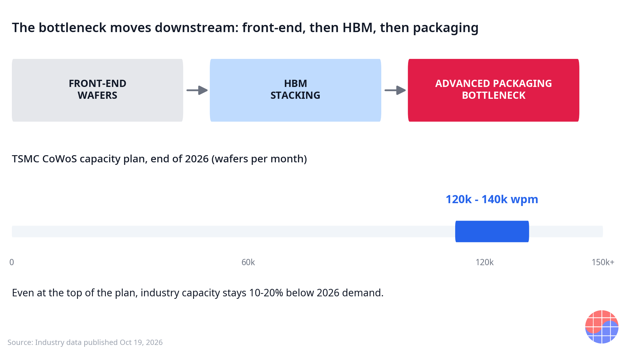
- TSMC plans to scale CoWoS capacity to roughly 120,000–140,000 wafers per month by the end of 2026. The largest single packaging build-out in the industry still does not close the gap.
- The structural read: the gap between advanced nodes and advanced packaging keeps pulling demand upstream into packaging equipment and materials. Thermal compression bonding (TCB) tools from equipment maker ASMPT have already been delivered to multiple OSATs, IDMs, and memory makers for HBM and chiplet-based production, with follow-on orders from AI computing customers disclosed.
- The business consequence is a power shift. When the scarce step is packaging, pricing power, allocation power, and customer lock-in move to whoever owns packaging capacity — and the reservation race for that capacity is already deciding 2026–2027 market share.
Background
Packaging used to be the cheap part
For most of semiconductor history, packaging was the commodity tail of the value chain. The front end — lithography, etch, deposition on advanced nodes — captured the prestige, the capital budgets, and most of the margin. Assembly and test were outsourced to OSATs (outsourced semiconductor assembly and test providers) precisely because the work was considered standardized, labor-intensive, and price-driven. Customers negotiated packaging contracts the way they negotiated logistics: on cost per unit, with multiple qualified vendors and little strategic anxiety.
That hierarchy is inverting. An AI accelerator is no longer a single die that gets wrapped in plastic. It is a system: a large logic die, several stacks of HBM (high bandwidth memory), and a silicon interposer that wires them together at bandwidths no conventional package can reach. TSMC's CoWoS (Chip-on-Wafer-on-Substrate) is the reference implementation of that architecture, and it has become the pacing item for AI server shipments. The chip is not finished when the wafer leaves the fab. It is finished when the package works — and packages are what the industry cannot build fast enough.
The 2026 numbers that frame the story
Industry data published on October 19, 2026 frames the year ahead with three numbers.
| Metric | 2026 figure | What it means |
|---|---|---|
| Advanced packaging share of the total OSAT market | More than 50% | The high end becomes the majority of the outsourced packaging business |
| Advanced packaging capacity vs. demand | 10–20% short | Even after expansion, one unit of demand in five to ten goes unmet at the margin |
| TSMC CoWoS capacity plan | 120,000–140,000 wafers per month by end-2026 | The biggest packaging ramp in the industry still leaves a gap |
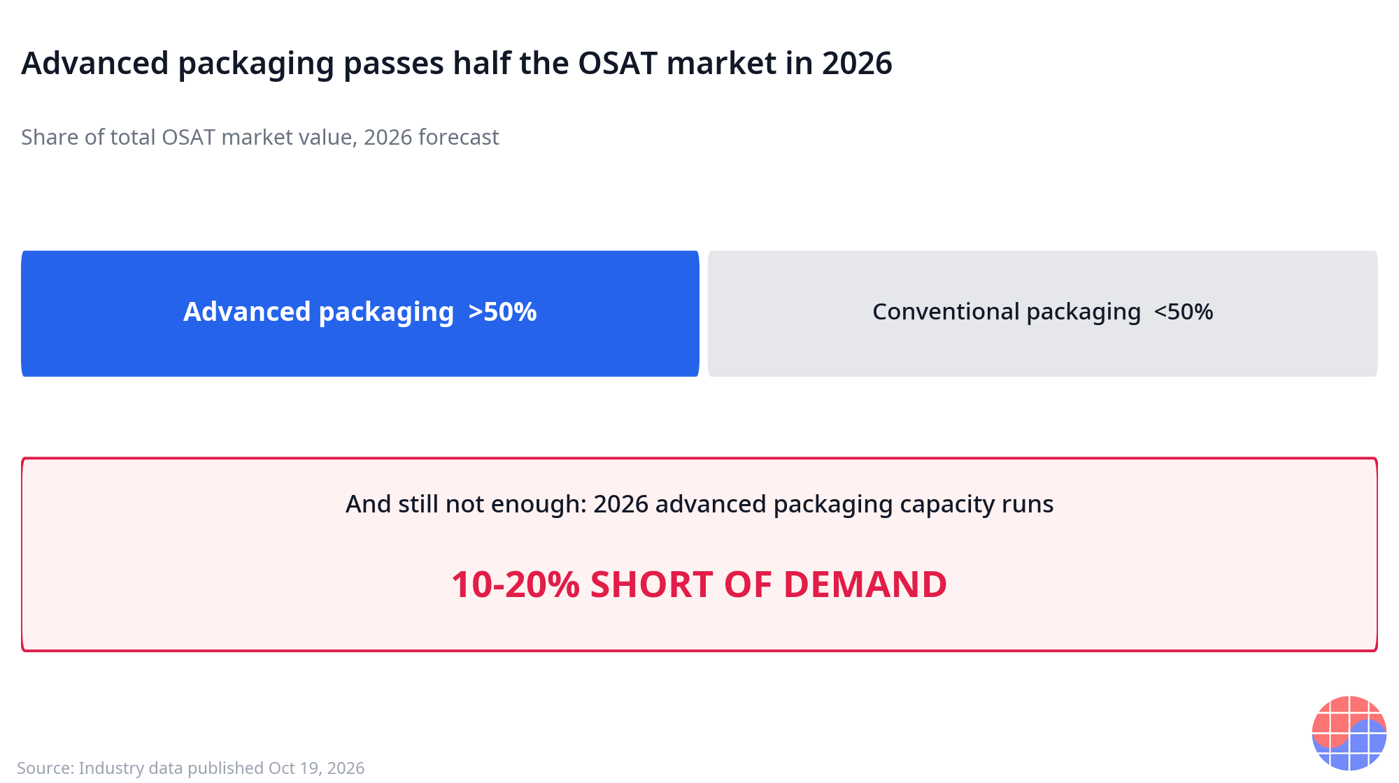
Source: industry data published October 19, 2026, reported October 20, 2026. Link in the footnote.
Two of these numbers deserve emphasis. The first is the majority crossing: when advanced packaging passes half of the OSAT market, the industry's center of gravity moves. Revenue pools, engineering talent, and capital spending follow the majority segment. The second is the persistence of the shortage at the peak of investment. A 10–20% shortfall in a year when the largest player is scaling its flagship packaging platform to 120,000–140,000 wafers per month is not a scheduling hiccup. It is a structural gap between how fast AI demand compounds and how fast packaging lines — tools, substrates, interposer wafers, and skilled process capacity — can be added.
Why packaging capacity is slow to add
Packaging lines look simpler than fabs, but the constraint stack is real. CoWoS-class capacity needs silicon interposer wafers (which compete for front-end fab slots), large ABF substrates, thermal compression bonders for stacking HBM and chiplets, and long qualification cycles before a line ships product a hyperscaler will accept. Each input has its own lead time and its own supplier bottleneck. The result is that advanced packaging capacity expands in steps, while AI accelerator demand has been compounding in curves. The 10–20% gap is what that mismatch looks like when it reaches 2026.
Business Deep Dive
The margin structure of the back end is being rewritten
The strategic significance of the majority crossing is not the headline share. It is what happens to the OSAT business model when the majority of its revenue pool is a scarce, yield-sensitive, engineering-heavy service instead of a commodity one.
Commodity packaging pricing is set by the cheapest qualified competitor. Scarce advanced packaging pricing is set by allocation: who gets capacity, in what quarter, at what priority. When capacity runs 10–20% short, the packaging provider stops being a vendor that customers squeeze and becomes a gatekeeper customers court. Multi-year capacity reservations, prepayments, and co-investment in dedicated lines — arrangements that used to belong to leading-edge wafer contracts — migrate into packaging agreements.
| Dimension | Conventional packaging era | Advanced packaging majority era |
|---|---|---|
| Pricing basis | Cost per unit, multiple qualified vendors | Allocation and reservation priority |
| Customer behavior | Annual tenders, price-first | Multi-year reservations, capacity pre-commitment |
| Supplier leverage | Low — switching is routine | High — qualifying a new packaging line takes quarters |
| Margin driver | Labor and utilization efficiency | Mix, yield, and scarcity |
| Strategic risk | Price wars in downcycles | Being locked out of capacity in upcycles |
This is the moment the back end stops being a cost center in the customer's spreadsheet and becomes a line item in the customer's strategy review. OSATs that own advanced capacity gain a seat at that table; OSATs that do not are left competing over the shrinking conventional half of the market, where the old price logic still applies.
Reservation is share: the capacity booking race
In a market running 10–20% short, the decisive commercial contest happens before any chip is packaged. It is the reservation contest. An AI platform owner that reserves CoWoS-class capacity for 2026 and 2027 has, in effect, pre-allocated its accelerator shipments for those years — and removed that capacity from every rival's plan. An owner that hesitates does not merely pay more; it ships less.
This dynamic rewards early, large, and credible commitments, and it punishes the wait-and-see procurement style that commodity packaging taught the industry. It also changes what "market share" means in AI silicon. Announced architectures do not ship; reserved packaging slots do. Analysts counting design wins without counting packaging reservations are measuring the wrong thing.
Foundry in-house vs. OSAT outsourced: the CoWoS split
The majority crossing also sharpens the industry's structural question: who should own advanced packaging?
TSMC's answer is visible in the CoWoS plan. Scaling to 120,000–140,000 wafers per month by the end of 2026 keeps the most valuable packaging platform inside the foundry, bundled with the logic wafer sale. The bundle is strategically powerful: the customer buys a finished, yield-managed path from tape-out to packaged accelerator, and the switching cost covers the whole path, not one process step.
The OSAT answer is flexibility and focus. Independent packaging specialists serve everyone — fabless designers, IDMs, and memory makers — and the 2026 shortage validates their investment case. Industry analysis points to exactly this tension: a structural gap between advanced nodes and packaging that keeps pulling demand toward whoever can add advanced lines fastest, whether that is a foundry's internal operation or an OSAT's.
The likely equilibrium is not winner-take-all. Foundry-integrated packaging anchors the largest AI platforms, where wafer and package are co-optimized. OSATs absorb the broadening wave behind them: chiplet-based products from second-tier designers, IDMs outsourcing overflow, and memory-adjacent packaging where HBM stacking and test expertise decide. A market where advanced packaging is the majority can feed both models — the shortage, paradoxically, is what makes room for everyone.
Picks and shovels: equipment and materials inherit the demand
Scarcity at the packaging step transfers demand upstream with unusual force, because adding capacity is equipment-limited. The clearest public signal is in bonding tools. ASMPT's thermal compression bonding equipment has been delivered to multiple OSATs, IDMs, and memory manufacturers for volume production of HBM and chiplet-based chips, and follow-on orders from an AI computing customer have been disclosed. TCB is the step that physically stacks HBM dies and bonds chiplets; when every packaging expansion plan needs more of it, the toolmaker's order book becomes a leading indicator for the whole back end.
The same logic runs through substrates, interposer capacity, underfill and molding materials, and test. A structural gap between advanced nodes and packaging — industry analysis expects it to persist — converts each of these input markets from a follower of front-end cycles into a direct beneficiary of AI demand. For investors who find accelerator valuations demanding, the packaging supply chain is where the same demand shows up with less narrative premium attached.
| Upstream segment | Why the packaging gap pulls it |
|---|---|
| TCB and bonding equipment | Every advanced line expansion needs stacking and bonding capacity; HBM and chiplet production are the reference use cases |
| ABF substrates and interposers | Larger packages consume more substrate area per chip; interposer wafers compete for fab capacity |
| Materials (underfill, mold, TIM) | Stacked, high-power packages raise material performance requirements per unit |
| Test and inspection | Stacked packages fail expensively; test intensity per package rises with value per package |
The Korea angle: HBM stacking and test are home turf
For Korea's semiconductor industry, the majority crossing lands on home turf. HBM is the memory at the center of the AI package, and Korean memory makers own the stacking, and much of the test, expertise that HBM production requires. An industry structure in which packaging is the scarce, value-capturing step raises the strategic weight of exactly the capabilities concentrated in Korea: HBM die stacking, advanced test, and the packaging investments Korean suppliers have been making around them.
It also reframes the questions Korean suppliers face. The issue is no longer only how much HBM wafer capacity to build, but how much of the packaging value chain — stacking, bonding, test, and the reservations that come with them — Korean players choose to own as the back end takes the majority. In a shortage market, the reservation contracts signed in 2026 will still be shaping shipment shares when today's headlines are forgotten.
Chase's Take
The lazy reading of this story is "packaging is hot." The correct reading is about where value pools sit when a supply chain's bottleneck moves.
For forty years the industry's scarcest, most defensible asset was the leading-edge wafer. Packaging was where margin went to be competed away. The 2026 data says the bottleneck has moved one step downstream, and everything reprices when a bottleneck moves: the gatekeeper changes, the contracts change, the investment logic changes. A market in which advanced packaging is both the majority of OSAT revenue and 10–20% undersupplied is a market where the back end sets the industry's shipping schedule.
Two implications are underappreciated. First, the reservation race quietly converts packaging capacity into future market share with a lag of four to eight quarters — by the time shipment data confirms it, the contest is already over. Second, the shortage is self-reinforcing for equipment and materials suppliers: every actor in the chain responds to the same 10–20% gap by ordering ahead, which is why bonding-tool deliveries and follow-on orders are the datapoints to watch, not the commentary.
The open question is duration. Shortages end — capacity always arrives eventually, and 120,000–140,000 wafers per month of CoWoS is a lot of arriving. But a structural gap between node advancement and packaging advancement does not close in one investment cycle, because the packaging constraint stack (interposers, substrates, bonders, qualification) renews itself at every node generation. The majority crossing is the part that does not reverse. Even when the shortage fades, advanced packaging stays the majority business — and the industry's center of gravity stays downstream with it.
Implications
- For AI platform owners: Packaging reservations are shipment plans. Treat CoWoS-class capacity booking with the same seriousness as wafer starts — in a 10–20% short market, an unreserved architecture is an unshipped one.
- For OSATs: The majority crossing is a once-in-a-generation repricing of the business model. The strategic task is converting today's allocation power into long-duration contracts and co-investment, not spot pricing wins.
- For foundries: In-house packaging at 120,000–140,000 wafers per month scale bundles the wafer and package into one switching cost. The bundle, not either step alone, is the moat.
- For equipment and materials suppliers: Bonding, substrates, and test inherit the demand. TCB deliveries to OSATs, IDMs, and memory makers — and follow-on AI orders — are the earliest hard evidence of each expansion wave.
- For investors: Track reservations and tool orders, not announcements. The signal that the gap is closing will appear in equipment lead times and substrate pricing before it appears in anyone's press release.
FAQ
Why is advanced packaging still short if TSMC is scaling CoWoS to 120,000–140,000 wafers per month?
Because demand is growing faster than the constraint stack can expand. CoWoS-class capacity needs interposer wafers, large substrates, thermal compression bonders, and long qualification cycles, each with its own bottleneck. Industry data published on October 19, 2026 forecasts advanced packaging to exceed 50% of the OSAT market in 2026 while capacity still runs 10–20% below demand.
What does it mean that advanced packaging passes 50% of the OSAT market?
It means the high end becomes the majority business of outsourced assembly and test. Revenue, capital spending, and engineering talent concentrate in advanced lines, the OSAT business model shifts from unit-cost competition toward allocation and reservations, and the conventional segment becomes the minority, price-driven half of the market.
What is thermal compression bonding (TCB), and why does it matter here?
TCB is the bonding process used to stack HBM dies and attach chiplets in advanced packages. Equipment maker ASMPT has delivered TCB tools to multiple OSATs, IDMs, and memory manufacturers for HBM and chiplet-based volume production, with follow-on orders from an AI computing customer disclosed — a sign that packaging expansion is equipment-limited and that tool orders lead capacity.
Who benefits from a 10–20% advanced packaging shortage?
Whoever owns the scarce capacity and the inputs to expand it: foundries with in-house advanced packaging, OSATs with advanced lines and reservation contracts, and the upstream equipment and materials suppliers — bonding tools, substrates, and test — whose order books fill first when everyone expands at once.
Source: Industry data on 2026 advanced packaging share, capacity gap, and CoWoS expansion plans (data published October 19, 2026; reported October 20, 2026). This article is analysis, not investment advice.
📩 Subscribe to VLSI Korea
Get our daily semiconductor deep-dives delivered to your inbox first. Free to subscribe.