VLSI Korea
Chipletz Deep Dive: The Smart Substrate That Deletes the Interposer
Chipletz began inside AMD in 2016 and spun out in 2021. CEO Bryan Black ran the die-stacking program behind Fiji, the first HBM product. Its Smart Substrate deletes the interposer and cut an HBM design from 16 metal layers to 9. SKC owns ~12%. Demo taped out; no production customer yet.


The 30-Second Summary
- Chipletz is an Austin, Texas fabless substrate startup that began in 2016 as a company-in-company inside AMD and spun out as an independent company in 2021. AMD and ASE, the world's largest outsourced assembly and test provider, remain its anchor shareholders.
- Its single product idea, the Smart Substrate, moves the fine-pitch die-to-die interconnect fabric, high-speed I/O and power delivery into the package substrate itself — deleting the silicon interposer that sits between the dies and the substrate in a conventional 2.5D package.
- The proof point on record: in Chipletz's own evaluation design with Siemens EDA tools, a very large SoC flanked by four HBM stacks (50 mm × 65 mm package, more than 180,000 device pins) needed 9 metal layers on a Smart Substrate versus 16 layers for the previous silicon-interposer revision.
- The company is led by Bryan Black, the AMD Senior Fellow who ran the die-stacking program behind Fiji, the first HBM product, in 2015. SKC joined as a strategic investor in September 2023 with a stake of about 12%. Round sizes beyond a recorded $9 million are undisclosed.
- Status as of October 2026: the first demonstration design has taped out and a second design is in progress, but no volume production customer has been publicly announced. Chipletz is a technology bet, not yet a business result — and this deep dive treats it that way.
Why the Substrate Became the Battlefield
For fifty years the package was plumbing: it protected the die and fanned signals out to the board. That era ended when transistor scaling stopped paying for system performance on its own. Performance now comes from putting more silicon in one package — compute chiplets, I/O dies and HBM stacks side by side — and the package decides how fast those dies can talk, how cleanly they are powered, and what the whole assembly costs.
The industry's default answer is the silicon interposer, perfected by TSMC's CoWoS: a slab of silicon, patterned with fine wiring and through-silicon vias, that carries every die-to-die signal. It works beautifully. It is also a wafer-sized piece of processed silicon that must be manufactured, tested and yielded for every package, and its capacity has been one of the binding constraints of the AI build-out. The interposer is, in effect, a second chip whose only job is to be a floor.
Chipletz's founding question is disarmingly simple: why buy the floor as silicon at all? A modern package substrate is already a multi-layer wiring structure. If the substrate itself could carry the dense, fine-pitch traffic between neighboring dies — and deliver cleaner power while doing it — the interposer, its cost, its capacity queue and its yield risk could all be removed from the bill of materials. That is the Smart Substrate thesis, and it is why the company's tagline is "The Substrate is your System."
Company Timeline
| Year | Milestone |
|---|---|
| 2015 | Bryan Black leads AMD's die-stacking program to launch with Fiji, the first HBM-equipped GPU — the industry's first high-volume interposer product |
| 2016 | Chipletz begins as a company-in-company (CIC) inside AMD in Austin, Texas |
| 2021 | Spin-out as an independent company; AMD and ASE become anchor shareholders |
| 2022 | First Smart Substrate design completed; Siemens EDA evaluation runs a very large SoC plus four HBM stacks on the technology |
| 2023 (Jan) | Siemens selected as strategic EDA provider (Xpedition Substrate Integrator, Xpedition Package Designer, HyperLynx, Calibre 3DSTACK) |
| 2023 (Sep) | SKC joins as strategic investor, taking a stake of about 12%; amount undisclosed |
| 2024 | Follow-on early-stage rounds recorded in company databases; amounts undisclosed. Initial product delivery to customers and partners had been targeted for early 2024 |
| 2025–2026 | First demonstration design tape-out completed and a second design iteration in progress (per Siemens EDA). Team of roughly 25 people. No publicly announced production design win as of October 2026 |
The People: Packaging Royalty, Not First-Timers
Startups in advanced packaging are usually founded by people who want to work on packaging. Chipletz was founded by the people who defined it.
Bryan Black, co-founder and CEO, spent more than two decades at Intel and AMD. As an AMD Senior Fellow he was the public face and technical lead of AMD's die-stacking effort — an eight-year program that shipped in 2015 as the Fiji GPU, the first product to combine a logic die and HBM stacks on a silicon interposer at consumer volume. When the industry talks about "the team that introduced HBM packaging," Black is one of the names it means. His later AMD talks on heterogeneous integration read like the Chipletz pitch written early: bridge approaches become interesting as interposers hit their limits, known-good-die has to be redefined, and integration — not transistors — is where performance comes from next.
Michael Su, co-founder and CTO, and Michael Alfano, VP of Product Engineering, come from the same packaging world, and the broader team is drawn from AMD veterans and other major system houses. This matters for what Chipletz sells. A substrate platform is not adopted because a datasheet looks good; it is adopted when a customer's packaging organization trusts the vendor to co-design a package that cannot fail. Chipletz's real asset is that its founders have personally taped out the packages everyone else now copies.
Smart Substrate, Anatomized
A conventional 2.5D package has three wiring tiers: the dies, a silicon interposer that carries the dense die-to-die traffic, and an organic substrate that fans everything out to the board and brings power in. The Smart Substrate collapses the middle tier into the third. Four elements make up the architecture:
1. Fine-pitch die-to-die fabric in the substrate. The dense, short-reach wiring that chiplets use to talk to each other — historically the interposer's exclusive job — is built as high-density routing inside the substrate, concentrated where dies sit adjacent to each other. Signals that need interposer-class density get it; the rest of the package does not pay for silicon it does not need.
2. High-speed external I/O. The same fabric carries fast off-package links to external compute modules and peripherals, so the package boundary stops being a bandwidth cliff.
3. Power as a designed feature, not an afterthought. Decoupling capacitors are integrated into the substrate itself, close to the dies, and the platform supports multiple voltage domains from a single supply — a mundane-sounding feature that removes real board-level cost and complexity, because dies from different vendors, built on different nodes, rarely want the same voltage. Power integrity is one of the quiet killers of multi-die products; Chipletz treats it as a first-class selling point ("cleaner power" is one of its three headline claims).
4. Vendor-neutral integration. The stated goal is to integrate "virtually any die from any manufacturer." Because Chipletz sells neither the dies nor the foundry process, it has no incentive to lock a customer into one silicon supplier — a structural difference from every incumbent packaging platform, each of which exists to pull wafers into its owner's fabs or assembly lines.
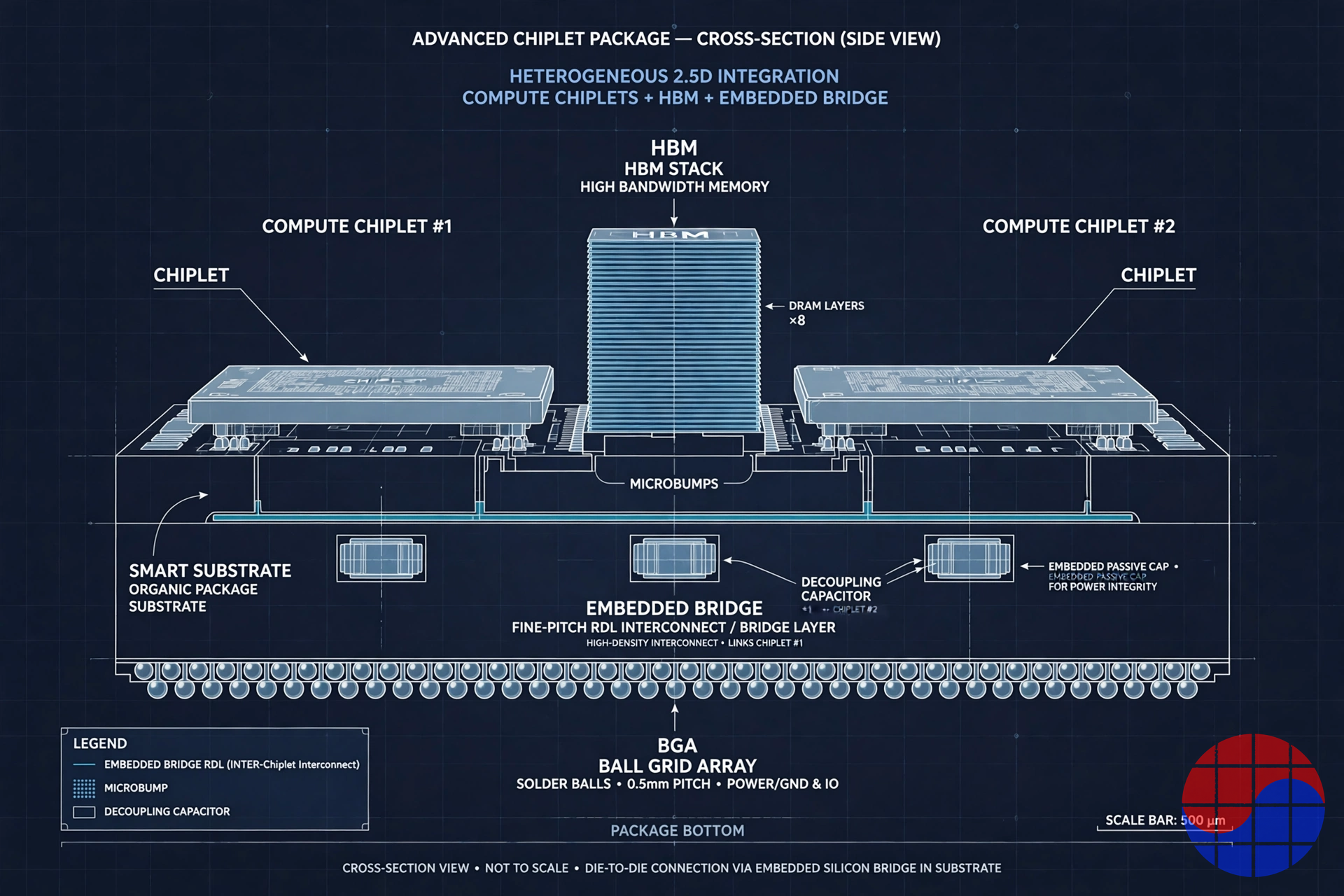
Cross-section concept of the Smart Substrate approach: the fine-pitch interconnect and decoupling capacitors live inside the substrate, so no separate interposer tier is needed. Source: VLSI Korea illustration.
The proof design, in numbers
Chipletz does not publish a datasheet, but its Siemens EDA evaluation design is on the record, and it is the most concrete technical evidence available:
| Metric | Smart Substrate evaluation design |
|---|---|
| Configuration | Very large SoC flanked by four HBM stacks |
| Package size | ~50 mm × 65 mm |
| Nets connecting the dies | 8,000+ |
| Vias | ~1.2 million |
| Total device pins | 180,000+ |
| BGA balls | 2,800 |
| Reuse circuits | 150+ |
| Metal layers — Smart Substrate design | 9 |
| Metal layers — previous silicon-interposer revision | 16 |
Read the last two rows carefully, because they are the whole business case in miniature. Metal layers are cost, cycle time and yield risk. An architecture that reaches the same system — same SoC, same four HBM stacks, same pin count — with roughly 44% fewer metal layers, and without consuming a large processed silicon interposer at all, attacks the two scarcest resources in AI hardware: packaging cost and packaging capacity. Chipletz's designs also operate at a planning scale far beyond manual methods: Siemens has described package designs in this class reaching toward 50 million pins of connectivity to plan and verify, which is why the EDA partnership is not a footnote but part of the product.
The Competitive Map: Four Ways to Wire a Package
Chipletz does not compete with "packaging." It competes with specific wiring strategies, each with a different owner and a different economic logic:
| Approach | How dies are wired | Die-to-die pitch / energy | Size & cost profile | Controlled by |
|---|---|---|---|---|
| Conventional organic substrate | Substrate routing only | ~100 µm-class bumps; ~1.7 pJ/bit | Cheapest; cannot carry dense chiplet traffic | Substrate makers, OSATs |
| Full silicon interposer (TSMC CoWoS-S) | One large silicon slab with TSVs under all dies | Micro-bump ~40 µm class; high density everywhere | Highest performance; interposer area grows with package, reticle limits require stitching; capacity-constrained | TSMC |
| RDL interposer with silicon bridges (TSMC CoWoS-L) | RDL carrier plus small silicon bridge chips (LSI) where density is needed | Bridge-class density at die edges | Cheaper than full interposer; still a separate interposer tier to build and attach | TSMC |
| Embedded bridge (Intel EMIB) | Small silicon bridges embedded directly in the organic substrate | 55 µm micro-bumps, ~45 µm in later generations; ~0.5 pJ/bit | No interposer; bridge placement is fixed at substrate manufacture | Intel |
| 3D hybrid bonding (TSMC SoIC) | Dies bonded face-to-face, copper to copper | 9 µm bond pitch at launch (2023), 6 µm in 2025 production | A different axis entirely: vertical stacking, not lateral wiring | TSMC |
| Smart Substrate (Chipletz) | Fine-pitch fabric, I/O and power built into the substrate; no interposer, no separate bridge tier | Detailed pitch figures not publicly disclosed | Targets interposer-class integration at substrate economics; adds integrated decoupling and multi-voltage power | Chipletz (fabless; manufactured with substrate partners) |
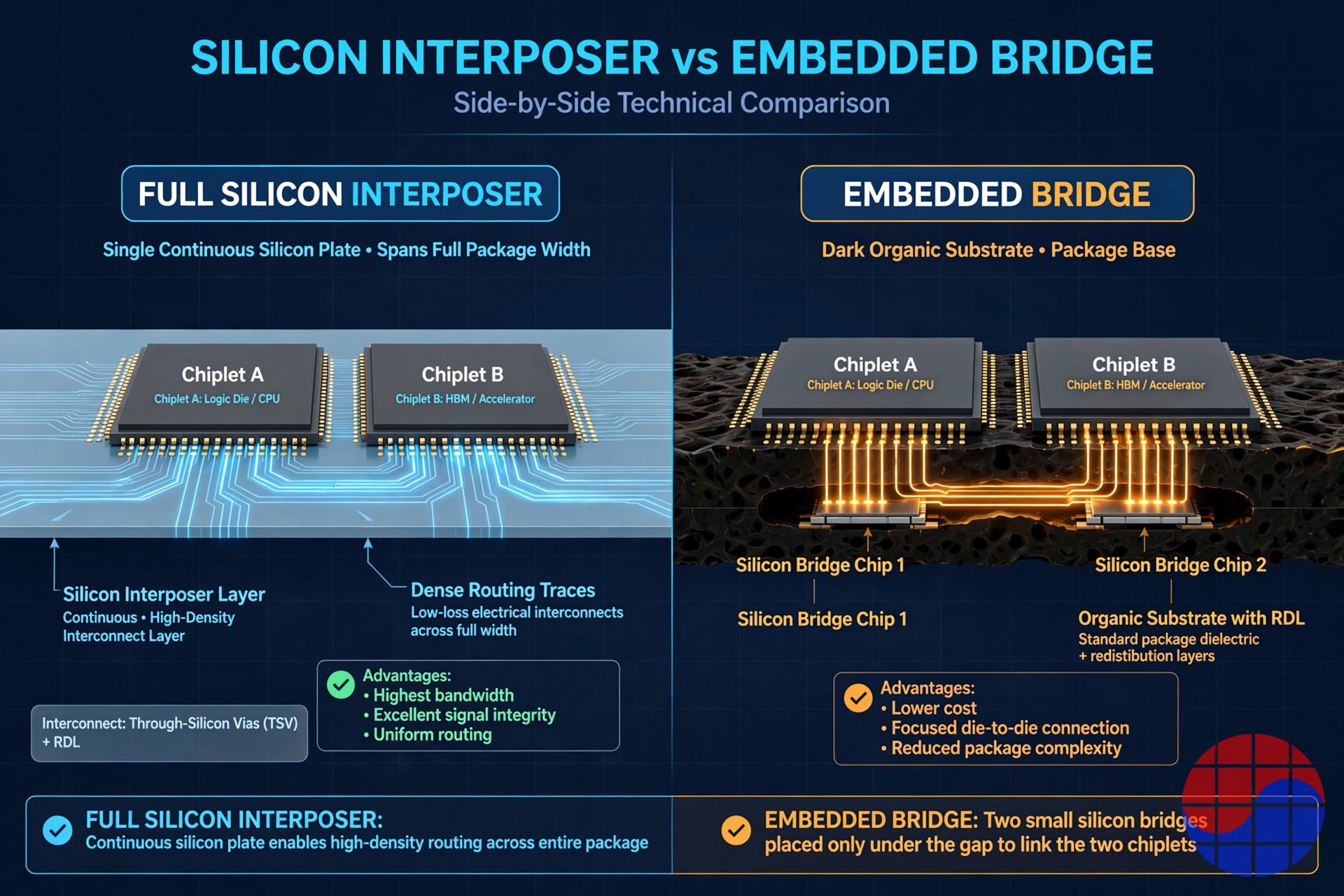
The economic fork in 2.5D packaging: pay for silicon across the whole package, or concentrate dense wiring at the die edges. Source: VLSI Korea illustration.
Two clarifications keep this map honest. First, EMIB is the closest relative — Intel proved a decade ago that embedding dense wiring in the substrate beats a full interposer on cost. Chipletz's differentiation is not the bridge idea itself; it is offering that class of integration as a vendor-neutral platform with the power architecture designed in, available to customers who are not Intel. Second, SoIC and hybrid bonding are not competitors but a different dimension: they stack dies vertically, while Chipletz wires them laterally. A future package can plausibly use both — hybrid-bonded stacks sitting on a Smart Substrate.
Not the same layer as Eliyan
Chipletz is often mentioned in the same breath as Eliyan, and the pairing confuses more than it clarifies. They sell different layers of the chiplet stack. Eliyan sells the electrical interface — die-to-die PHY IP (its NuLink PHY has demonstrated 64 Gbps per bump) that lets two dies speak to each other, and it works on standard packaging as well as advanced substrates. Chipletz sells the physical medium — the substrate platform the signals travel through and the power network that feeds the dies. A PHY without a route is useless; a route without a PHY is silent. The two are complements that get lumped together because both are "chiplet startups," and any serious map of the ecosystem should keep the layers separate: PHY IP at the top, the interconnect medium in the middle, foundry and OSAT manufacturing at the bottom.
Money and Shareholders
Chipletz's cap table is more informative than its (mostly undisclosed) round sizes:
| Item | Detail |
|---|---|
| Anchor shareholders | AMD (originator) and ASE (world's largest OSAT) hold leading stakes from the spin-out |
| Recorded round (Sep 2023) | $9 million recorded in company databases alongside SKC's entry; round naming differs between sources (SKC describes its participation as a Series B) |
| SKC (Sep 2023) | Strategic investor; about 12% stake after the round; amount undisclosed by confidentiality agreement |
| Follow-on rounds | Further early-stage rounds recorded in February and November 2024; amounts undisclosed |
| Valuation | Not publicly disclosed |
The SKC investment deserves a paragraph, because it explains Chipletz's most plausible route to manufacturing scale. SKC is the Korean materials group behind Absolics, which built a glass-substrate fab in Georgia, USA — one of the highest-profile bets on next-generation substrate materials. SKC said explicitly that it wants to combine its substrate production capacity with Chipletz's engineering know-how and customer network to build a differentiated "chip packaging solution ecosystem," including joint responses to the US CHIPS Act. In other words: Chipletz brings the architecture and the design wins; partners like SKC/Absolics and ASE bring factories. That is what "fabless substrate" means in practice — Chipletz is to substrates what a fabless chip company is to wafers.
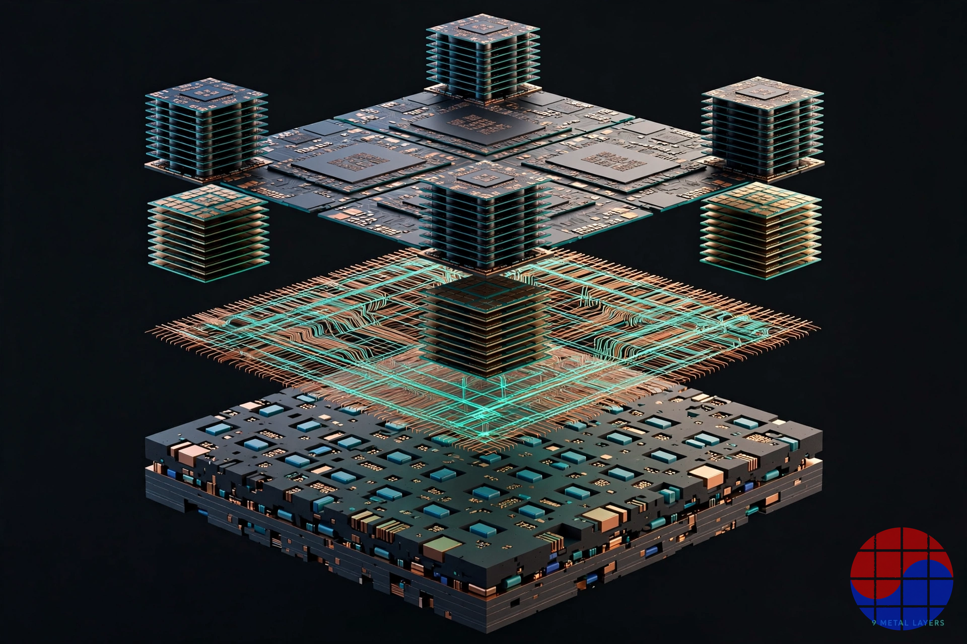
Exploded view of the integration stack Chipletz wants to own: dies, interconnect fabric and a power-aware substrate. Source: VLSI Korea illustration.
Adoption Reality and Risks
A premium deep dive owes the reader the bear case in the same detail as the bull case. Five risks define Chipletz's actual position in October 2026:
1. No public production win. The company's own early target — initial products to customers and partners in early 2024 — has passed without a publicly announced volume design win. A completed demonstration tape-out and a second design iteration show the technology is real; they do not show it is adopted. In packaging, the distance between those two states is measured in years of qualification.
2. The customer list is the industry. The buyers who need interposer-class integration at scale are a handful of hyperscalers and chip giants, and most of them are vertically committed: NVIDIA and AMD volumes flow through TSMC's packaging roadmap, Intel pushes its own EMIB/Foveros stack, and Broadcom and Marvell have deep foundry alignments. A neutral platform is most attractive to the second tier — AI ASIC startups, defense and specialty HPC — which is a real market but a slower one.
3. Fabless cuts both ways. Chipletz does not own substrate capacity. Its model depends on partners (SKC/Absolics on materials, ASE on assembly) executing a novel substrate at yield, at volume, on someone else's roadmap priorities. Every partner is also a potential competitor or a distraction away from deprioritizing the program.
4. Small team, long cycles. Roughly 25 people is a design-house scale, not a platform-company scale. Each customer engagement is a multi-quarter co-design effort; the company can only run a few in parallel, so one slipped program is a material event.
5. The incumbents are absorbing the idea. CoWoS-L already concedes the core insight — most of the package does not need silicon-density wiring — and Intel has productized embedded bridges for years. Chipletz must stay ahead of two of the best-funded engineering organizations on earth, on their home turf, while they bundle packaging with the wafers and assembly the customer is buying anyway.
Chase's Take
Three judgments, in descending order of confidence.
First, the thesis is right and early, not wrong. The interposer is a transitional technology — a brilliant one, but a bridge (in the historical sense) between the era when substrates could not route and the era when they can. Every cost curve in the industry points toward pushing function down into the substrate and panel-level manufacturing. Black identified this from inside AMD before almost anyone; the Fiji program he ran is precisely what taught him the interposer's limits.
Second, Chipletz's fate will be decided by partners, not by physics. The technology evidence — a 50 × 65 mm, four-HBM design at nine metal layers — is credible and comes with Siemens' name attached. What is missing is not proof but a production flag planted by a named customer on a partner's line. Watch the SKC/Absolics axis: if a Smart Substrate design ever tapes out on a glass-substrate roadmap in Georgia, the fabless-substrate model stops being a pitch and becomes a supply chain.
Third, the most likely endgame is strategic, not IPO. A ~25-person company holding the architecture, the EDA flow know-how and the trust of the exact people who buy advanced packaging is worth more inside a substrate maker, an OSAT or an EDA-adjacent platform than as a standalone. AMD and ASE already sit on the cap table; SKC bought its option in 2023. The question is not whether the Smart Substrate idea gets absorbed into the industry's substrate roadmap — it will be — but whether Chipletz's shareholders capture that value through adoption first, or through an acquisition that prices the team and the IP. Either way, "the substrate is the system" has already won as an idea. The open question is only who gets paid for it.
FAQ
Q: What is Chipletz? A: Chipletz is an Austin, Texas-based fabless substrate startup, spun out of AMD in 2021 after starting as an internal AMD venture in 2016. Led by CEO Bryan Black, it develops the Smart Substrate, a package substrate with built-in fine-pitch chiplet interconnect, high-speed I/O and power delivery that removes the need for a silicon interposer.
Q: How is the Smart Substrate different from TSMC CoWoS or Intel EMIB? A: CoWoS places all dies on a separate silicon interposer (CoWoS-S) or an RDL interposer with embedded silicon bridges (CoWoS-L); Intel EMIB embeds small silicon bridges in the substrate, but only as part of Intel's own packaging platform. The Smart Substrate builds the dense die-to-die fabric, I/O and power — including integrated decoupling capacitors and multiple voltage domains from one supply — directly into a vendor-neutral substrate platform sold by an independent company.
Q: Who has invested in Chipletz? A: AMD and ASE are anchor shareholders from the 2021 spin-out. In September 2023, South Korea's SKC joined as a strategic investor with a stake of about 12%, with the amount undisclosed; company databases record a $9 million round at that time and further early-stage rounds in 2024, also undisclosed. Total funding and valuation are not public.
Q: Is the Smart Substrate in production? A: Not in publicly announced volume production as of October 2026. Chipletz completed its first Smart Substrate design in 2022, its first demonstration design has taped out, and a second design iteration is in progress with Siemens EDA tools. No production customer has been named publicly.
Q: Who is Bryan Black? A: Bryan Black is Chipletz's co-founder and CEO, a packaging expert with more than 20 years at Intel and AMD. As an AMD Senior Fellow he led the die-stacking program behind Fiji (2015), the first GPU to ship with HBM on a silicon interposer, and he is regarded as one of the foremost authorities on 3D and heterogeneous integration.
Sources: Chipletz and Siemens EDA announcements and case study material; SKC press release (September 2023); Korean and international business press coverage of the SKC investment; PitchBook company profile (accessed October 2026). Funding amounts and the company valuation are as disclosed by those sources; undisclosed figures are marked as such. This article is analysis, not investment advice.
📩 Subscribe to VLSI Korea
Get our daily semiconductor deep-dives delivered to your inbox first. Free to subscribe.