VLSI Korea
The Glass-Core Substrate Race: Why Glass Is the Next Packaging Paradigm After ABF
As AI packages outgrow ABF cores on warpage, glass-core substrates move from research to a qualification race. Timelines for Intel, TSMC, SEMCO, Absolics and LG Innotek, the TGV engineering hurdles, and Korea's display-glass edge.


The Glass-Core Substrate Race: Why Glass Is the Next Packaging Paradigm After ABF
TL;DR
The core material of advanced package substrates is starting to change. As AI packages grow larger, the organic ABF core is hitting a warpage limit, and glass — whose coefficient of thermal expansion (CTE) can be tuned close to silicon, with better flatness and dimensional stability — has emerged as the leading successor material. As of October 20, 2026, no glass-core substrate is in volume production: reported volume targets cluster between the second half of 2027 and 2030. Intel presented its glass substrate research in September 2023 and showed a first sample combining EMIB with a glass core at NEPCON Japan on January 22, 2026, as reported. The winners will be decided less by who announces first and more by who passes qualification with an anchor AI customer — and Korean suppliers including Samsung Electro-Mechanics, Absolics (SKC), and LG Innotek hold an unusually strong hand because of Korea's display-glass heritage.
Background
A package substrate is the board between a chip and the printed circuit board. It fans out the chip's dense connections into a form the rest of the system can use, and its core material determines how large, flat, and finely wired that package can be. For the past generation of high-end computing, that core has been organic — most notably the ABF build-up film stack used in large CPU and AI accelerator packages.
That worked while packages were moderate in size. AI accelerators changed the geometry: a modern AI package combines a large logic die with multiple HBM stacks on an interposer, and each generation pushes total package area further out. As the package grows, the substrate underneath has to stay flat across a wider span, hold finer wiring over that span, and survive repeated thermal cycles without bending enough to break solder joints or stress the dies above it.
This is the context in which glass has moved from a research curiosity to an industry race. Glass is not new as an industrial material — display manufacturing has handled very large glass panels at scale for decades. What is new is using glass as the core of a package substrate, drilled with through-glass vias (TGV) that carry signals and power vertically through the core. Through 2023 and 2024, glass-core work was mostly research disclosure; from 2025 onward, as reported across company announcements, it has become pilot lines, joint ventures, and dated volume-production targets.
A note on scope: a separate, shorter-term story exists around ABF substrate supply and pricing. This article is not about that. It is about the longer transition of the core material itself — its timing, its qualification hurdles, and its engineering risks.
Deep Dive 1: Why Glass — Warpage, CTE, and Fine Wiring
The case for glass rests on three physical properties.
First, warpage. When materials with different thermal expansion rates are bonded together and heated, the stack bends. An organic core expands at a rate quite different from silicon, so a large package built on it tends to bow as it is processed and as it heats and cools in operation. The larger the package, the worse the bending — and AI packages are the largest packages the industry has ever built. Glass can be formulated so that its CTE sits much closer to silicon's. A core that expands at nearly the same rate as the dies mounted on it stays flatter, which protects bump joints and allows still larger packages to be assembled with acceptable yield, as company disclosures describe the rationale.
Second, flatness and dimensional stability. Glass is rigid and smooth. A rigid core does not flex during processing, and its dimensions stay stable, which matters when thousands of fine connections must land in exactly the right place across a wide area. Organic cores, by contrast, can shift and deform slightly during manufacturing, and that movement becomes a yield problem as wiring density rises.
Third, fine wiring through TGV. In a glass core, vertical connections are formed as through-glass vias — holes drilled through the glass and metallized. Because glass is an excellent electrical insulator and dimensionally stable, TGV structures support dense, fine-pitch interconnect through the core itself. Intel, presenting its glass substrate research in September 2023, pointed to a path toward roughly ten times the interconnect density of organic substrates later this decade, as the company presented it. That density path is the strategic prize: more bandwidth between chiplets, more power delivery through the core, and more design freedom for very large multi-die packages.
Deep Dive 2: The Players and Their Reported Timelines
Four groups are racing, with different starting points.
Intel was first to disclose. The company presented its glass-core substrate research in September 2023, framing glass as a technology for the later part of this decade. On January 22, 2026, at NEPCON Japan, Intel showed what was reported as its first sample combining EMIB — its embedded bridge interconnect — with a glass core: a chip at twice reticle size with a 45µm bump pitch, with no micro-cracks found in testing, as reported from the event. The combination matters. EMIB already places silicon bridges inside a substrate; putting that approach on a glass core is a statement that glass is meant to carry Intel's most advanced packaging architecture, not a side experiment.
TSMC is approaching glass through panel-level packaging. Its CoPoS platform is built around a 310×310mm panel format, with a pilot line at its subsidiary VisEra, trial production in 2027, and a volume-production target of the second half of 2028, as reported from the company's roadmap disclosures. TSMC's entry matters because its customers define the AI package roadmap: if the largest foundry's panel platform adopts a glass core path, qualification demand follows.
Samsung Electro-Mechanics (SEMCO) is Korea's most advanced entrant in glass core substrates specifically. It operates a pilot line in Sejong. In November 2025, in Tokyo, a glass-core joint venture with the Sumitomo Chemical Group (Dongwoo Fine-Chem) was announced, as reported, combining substrate manufacturing with glass materials expertise. SEMCO's reported volume-production target is the second half of 2027, and customer qualification work with customers including Broadcom has been reported — the detail to watch, since pilot lines prove a process can run while qualification proves a customer will bet a product on it.
Absolics, an SKC subsidiary, is the most aggressive pure-play. Its plant in Covington, Georgia, in the United States, positions glass substrates inside the US supply chain. The company presents thickness and power advantages over organic substrates, as the company claims. In 2026, as reported, SKC carried out a 1.2 trillion won capital raise and an additional 589.6 billion won investment into Absolics, and prototype projects with US customers have been reported. Absolics' reported timeline points to 2027.
LG Innotek is developing glass substrates with UTI, with volume production reported as targeted for 2027–2028. Separately, Samsung Electronics has been reported to be reviewing glass interposers — a related but distinct component, covered in the next sections.
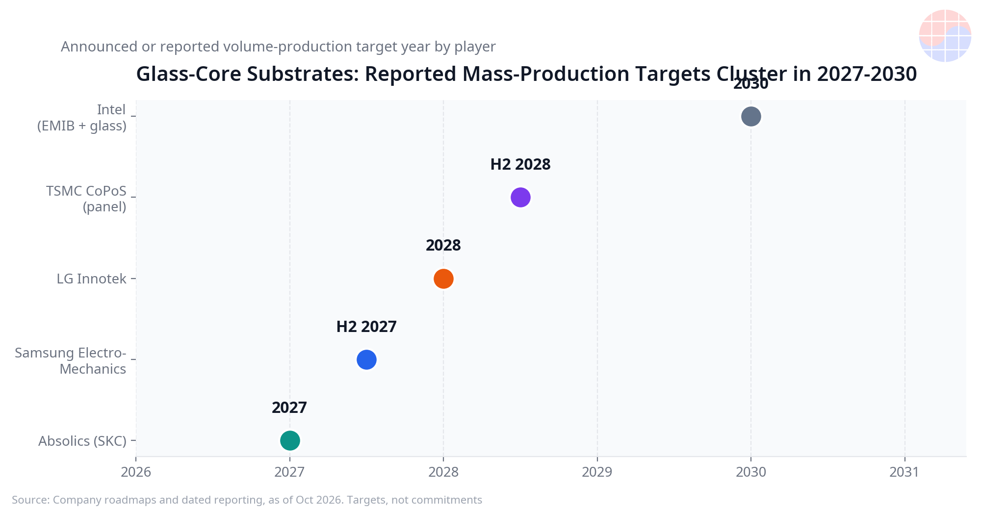
Read the timeline honestly: every volume target sits between 2027 and 2030, and none has been met yet. Announced targets in substrate programs have a history of slipping when qualification or yield runs long.
Deep Dive 3: Panel Formats — Why Size Is the Whole Point
Glass-core substrates and panel-level packaging advance together, because both are answers to the same problem: packages are outgrowing round wafers and small substrates.
The arithmetic is simple geometry. A 300mm round wafer offers about 70,686 mm² of area. TSMC's CoPoS panel at 310×310mm offers 96,100 mm² — and, being rectangular, it wastes far less of that area on rectangular packages than a circle does. A 600×600mm panel format, of the kind display-glass infrastructure already knows how to handle, offers 360,000 mm². Each step up in format multiplies the packages produced per pass through the line, which is how unit costs fall — geometry, not forecast.
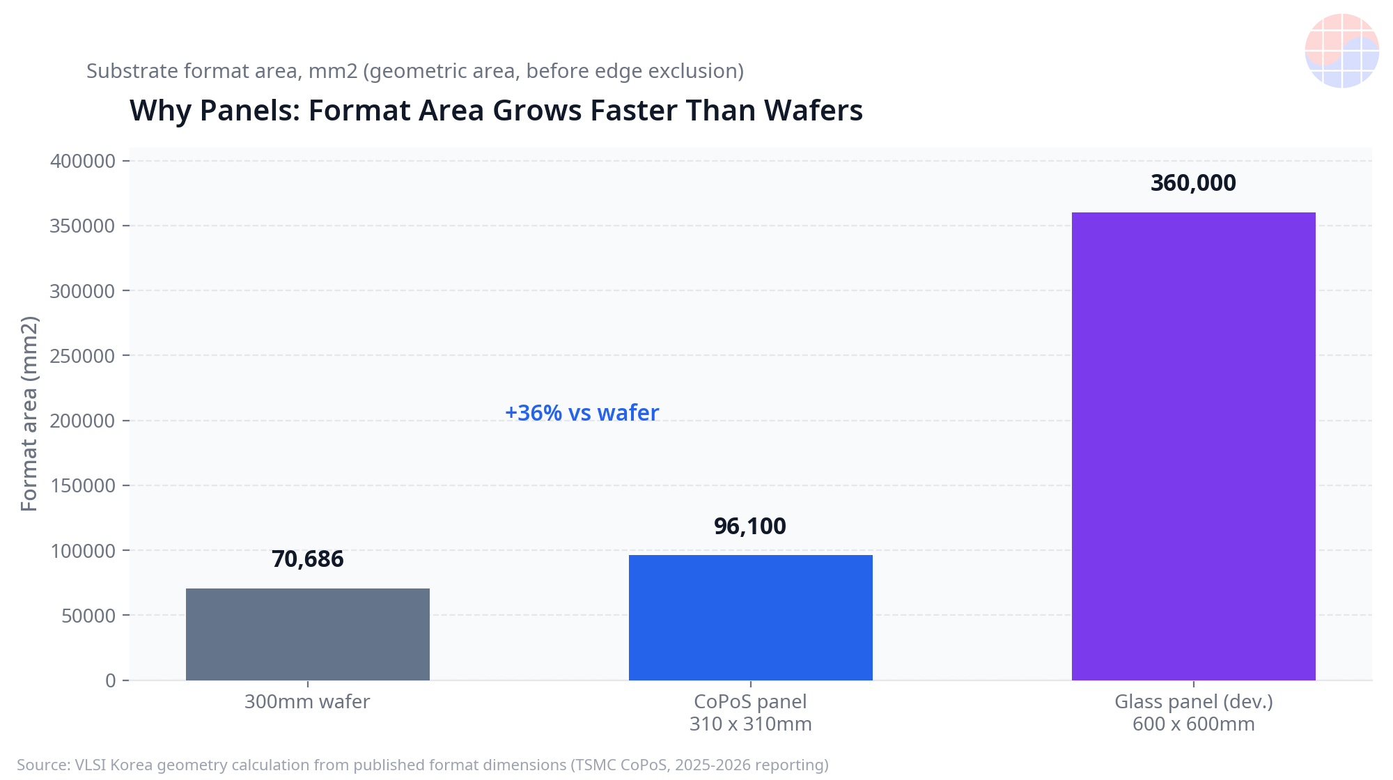
This is where Korea's industrial heritage becomes relevant. Handling large, thin, fragile glass sheets without breaking them — moving them, aligning them, processing them, inspecting them — is precisely the competence Korea's display industry built over decades. Panel formats are not just a packaging decision; they are a decision about which country's existing factory skills transfer.
Size also cuts the other way: a larger glass panel concentrates more value into a single fragile sheet, and every handling step is a chance to lose it.
Deep Dive 4: The Honest Hurdles — Brittleness, Yield, and an Immature Ecosystem
Glass has real weaknesses, and any credible account of this race has to price them in.
Brittleness is the first. Glass does not bend; it cracks. A glass core that survives the fab must also survive assembly, shipping, board mounting, and years of thermal cycling in a data center. Edge defects and micro-cracks invisible at inspection can propagate later. Intel's January 2026 sample result — no micro-cracks found in testing, as reported — is encouraging precisely because cracking is the known failure mode everyone is watching.
TGV yield is the second. Drilling and metallizing vast numbers of fine vias through glass, without micro-cracks around the via walls and with reliable copper fill, is a yield problem that compounds: one large substrate carries enormous numbers of vias, and it is only good if essentially all of them are. Via-related yield, not the glass sheet itself, may be the true gate to volume production.
The third hurdle is the ecosystem. Organic substrates benefit from decades of mature handling equipment, inspection tools, materials, and operator know-how. Glass-core ecosystems are still immature by comparison: carriers, handling methods, drilling and plating equipment, and inspection standards are all being built alongside the product itself — and immature ecosystems make timelines slip in ways press releases never show.
The fourth point is competitive, and it cuts against a simple displacement story. The incumbent ABF substrate makers — Ibiden, Shinko Electric Industries, and Unimicron — are themselves investing in glass. Glass therefore arrives first as a complement at the very top of the package stack, where warpage is intolerable, while organic cores continue below that tier. Replacement, if it comes, will be gradual and layered, not a single switchover. And with volume targets clustered in 2027–2030, every program in this race carries slippage risk: a single failed qualification round can move a target by a year.
Chase's Take
The way to read this race is that the substrate is stopping being a commodity. For decades it was a relatively passive carrier — specified, sourced, and largely invisible in the value chain. A glass core changes that: when the core material determines maximum package size, interconnect density, and panel format, the substrate becomes a platform layer on which the customer's whole multi-die architecture depends.
Value migrates accordingly — toward whoever owns the glass core, the TGV process, and the panel ecosystem around them, as a bundle. Selling glass sheets alone captures little. Selling a qualified glass-core platform, with via process and panel handling already proven at a customer's fab, captures a position that is hard to displace, because re-qualifying a substrate platform is slow and risky for the customer.
Korea's hand is unusual, and it comes from display glass. SEMCO brings substrate manufacturing and a materials joint venture; Absolics brings a US plant, a committed parent in SKC, and a pure-play focus; LG Innotek brings precision component manufacturing. All three stand on national process heritage in handling large glass. But heritage is not a purchase order: one anchor AI customer's qualification decision will do more to decide the winners than any pilot line or press release — which is why reported qualification work, such as SEMCO's with Broadcom, matters more than announced capacity.
One distinction is worth keeping precise, because the two roles are often confused. Samsung Electro-Mechanics is the glass core substrate player: the substrate is its product. Samsung Electronics, separately, has been reported to be reviewing glass interposers — the interposer is a different component, sitting between the dies and the substrate. Two Samsung names, two different layers of the package, two different competitive contests.
My base case: glass cores enter at the top of the AI package stack in the 2027–2028 window through one or two anchor qualifications, coexist with ABF cores for years, and expand downward only as TGV yield and the handling ecosystem mature. The race is real, but it will be scored on qualification certificates, not announcements.
Implications
- For AI package roadmaps: glass-core availability in the 2027–2028 window, if qualification succeeds, relaxes the warpage ceiling on package size — enabling larger multi-die designs.
- For substrate incumbents: Ibiden, Shinko Electric Industries, and Unimicron investing in glass signals complement-first, not displacement — ABF capacity stays strategically relevant through the transition.
- For Korean suppliers: SEMCO, Absolics (SKC), and LG Innotek convert display-glass heritage into a packaging position, but anchor-customer qualification — not capacity announcements — converts position into revenue.
- For investors: reported volume targets cluster in 2027–2030 with slippage risk; the verifiable checkpoints are qualification announcements and pilot-line yield disclosures, not target dates.
- For equipment and materials suppliers: the immature glass handling, drilling, plating, and inspection ecosystem is itself an opportunity — the picks-and-shovels layer of this transition is still being built.
This article is an independent analysis based on company disclosures and dated public reporting as of October 20, 2026; reported targets and claims are attributed to their sources and may change.
FAQ
Q: When will glass-core substrates reach volume production? A: As of October 20, 2026, reported targets cluster between the second half of 2027 and 2030: Absolics points to 2027, Samsung Electro-Mechanics targets the second half of 2027, LG Innotek targets 2027–2028, TSMC's CoPoS targets the second half of 2028, and Intel frames glass for later this decade. All carry slippage risk.
Q: Will glass replace ABF substrates entirely? A: Not on any near-term reading of the evidence. The incumbent ABF makers — Ibiden, Shinko Electric Industries, and Unimicron — are themselves investing in glass, which points to glass entering first as a complement for the largest, most warpage-sensitive packages while organic cores continue elsewhere.
Q: Why does glass help with warpage and fine wiring? A: Glass can be formulated with a CTE close to silicon, so a large package expands more uniformly and stays flatter than on an organic core. Its rigidity and dimensional stability also support fine wiring, and through-glass vias (TGV) carry dense vertical interconnect through the core.
Q: Which Korean companies are involved, and how do Samsung Electro-Mechanics and Samsung Electronics differ? A: Samsung Electro-Mechanics (pilot line in Sejong, glass-core joint venture announced in November 2025, volume target of the second half of 2027), Absolics of SKC (Covington, Georgia plant), and LG Innotek (developing with UTI) are the Korean substrate players. Samsung Electro-Mechanics makes glass core substrates; Samsung Electronics has separately been reported to be reviewing glass interposers, a different component.
📩 Subscribe to VLSI Korea
Get our daily semiconductor deep-dives delivered to your inbox first. Free to subscribe.