VLSI Korea
HBM 8-High vs 12-High vs 16-High: Who Profits as Stacks Get Taller
HBM 8-high vs 12-high vs 16-high — stack height is not a spec, it is a price tag. Cum yield falls 85% to 79% to 72% (KGD 98%): thinning (~30 um), the bonding transition, and no post-stack rework are the bottlenecks. Who profits from tall vs short stacks.


TL;DR: HBM stack height is not a spec number — it is where the money flows. Moving from 12-high to 16-high stresses every process step at once — DRAM die yield, wafer thinning, bonding, and testing — and cumulative stack yield falls from 85% at 8-high to 79% at 12-high to 72% at 16-high (assuming 98% KGD). That is why high stacks let the first mover capture the premium (SK hynix took about half of HBM revenue in H1 2026), while short stacks favor NVIDIA and the cloud vendors that ship more GPUs, plus Chinese followers who can only make yield work at 8-high. The three core bottlenecks are the thinning limit (~30 µm), the bonding transition (hybrid bonding), and the fact that a finished stack cannot be reworked.
Why stack higher — the interposer area is fixed
An AI accelerator's package area is effectively fixed. The number of HBM sites beside the GPU die is set by physics (Vera Rubin: 8 HBM4 sites), and growing the interposer breaks both yield and cost. With area fixed, the only way to add capacity and bandwidth is to build upward.
The numbers are clear. A 12-high HBM3E stack delivers about 1.2 TB/s and 36 GB on a 1,024-bit interface at 9.6 Gbps. HBM4 doubles the interface to 2,048 bits, so a 12-high stack holds 36 GB at over 2 TB/s. Same eight sites, a whole generation of capacity and bandwidth gained. 16-high HBM4 reaches 48 GB per stack using 32 Gb dies (the part SK hynix showed at CES 2026). Stack height is a density game: how much memory and bandwidth you extract from the same footprint.
It is also a system-TCO game. More capacity per GPU package means serving the same model with fewer GPUs, cutting GPU-to-GPU communication (NVLink, scale-up fabric) overhead. In the inference era, HBM stack height is one of the most reliable levers for lowering cost per token.
What each height demands — 8, 12, and 16-high are different processes
8-high — the mature zone. DRAM dies have thickness margin, and conventional TC (thermo-compression) bonding with NCF (non-conductive film) prints them reliably. 8-high HBM3E at 24 GB was the Blackwell workhorse and remains the easiest point on yield and cost. The technical hurdles are low, but it loses the density race.
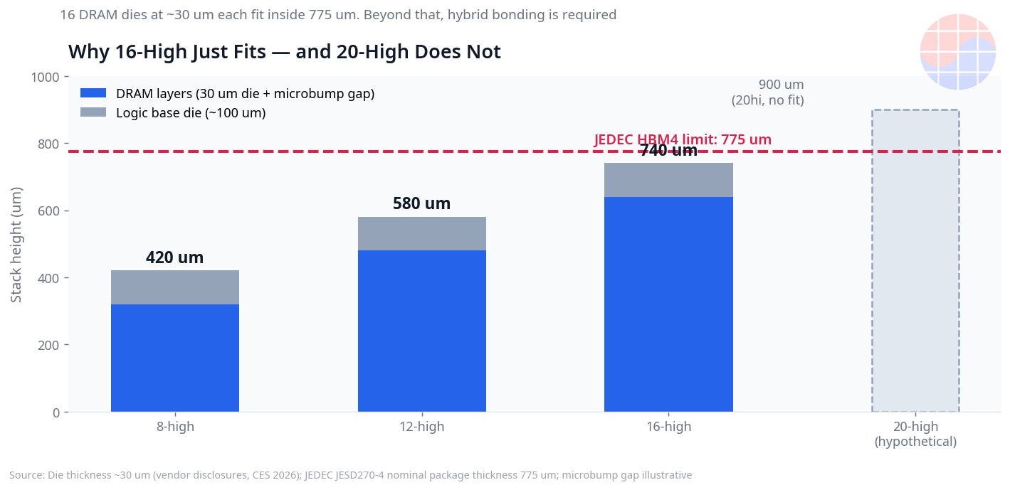
12-high — today's main battlefield. JEDEC JESD270-4 (the HBM4 standard, April 2025) sets package height at 775 µm for both 12-high and 16-high. Fitting 12 dies inside means thinning DRAM to about 30 µm and leveling up TSV (through-silicon via) formation, thin-wafer handling, and warpage control all at once. SK hynix began volume shipments of 12-high HBM4 to NVIDIA in late June 2026 using Advanced MR-MUF (mass reflow molded underfill); Samsung announced HBM4 mass production on February 12, 2026 (4 nm logic base die, 12-high, 3.3 TB/s). The base die is now standardly built on TSMC logic processes (3 nm/4 nm-class), not DRAM processes. Micron has been shipping HBM4 since March 2026.
16-high — the thinning-limit zone. JEDEC's decision to hold 775 µm created room for 16-high on existing bonding technology. At CES 2026, SK hynix showed a 48 GB HBM4 fitting 16 dies — each thinned to about 30 µm — inside 775 µm. But at 16-high, die-handling breakage, stack warpage, and heat dissipation all hit their limits simultaneously. Samsung is pushing further toward bumpless hybrid bonding for 16-high, while SK hynix counters by advancing MR-MUF. As of October 2026, no HBM product has shipped in volume using hybrid bonding.
Why it has to be expensive — the math of cumulative yield
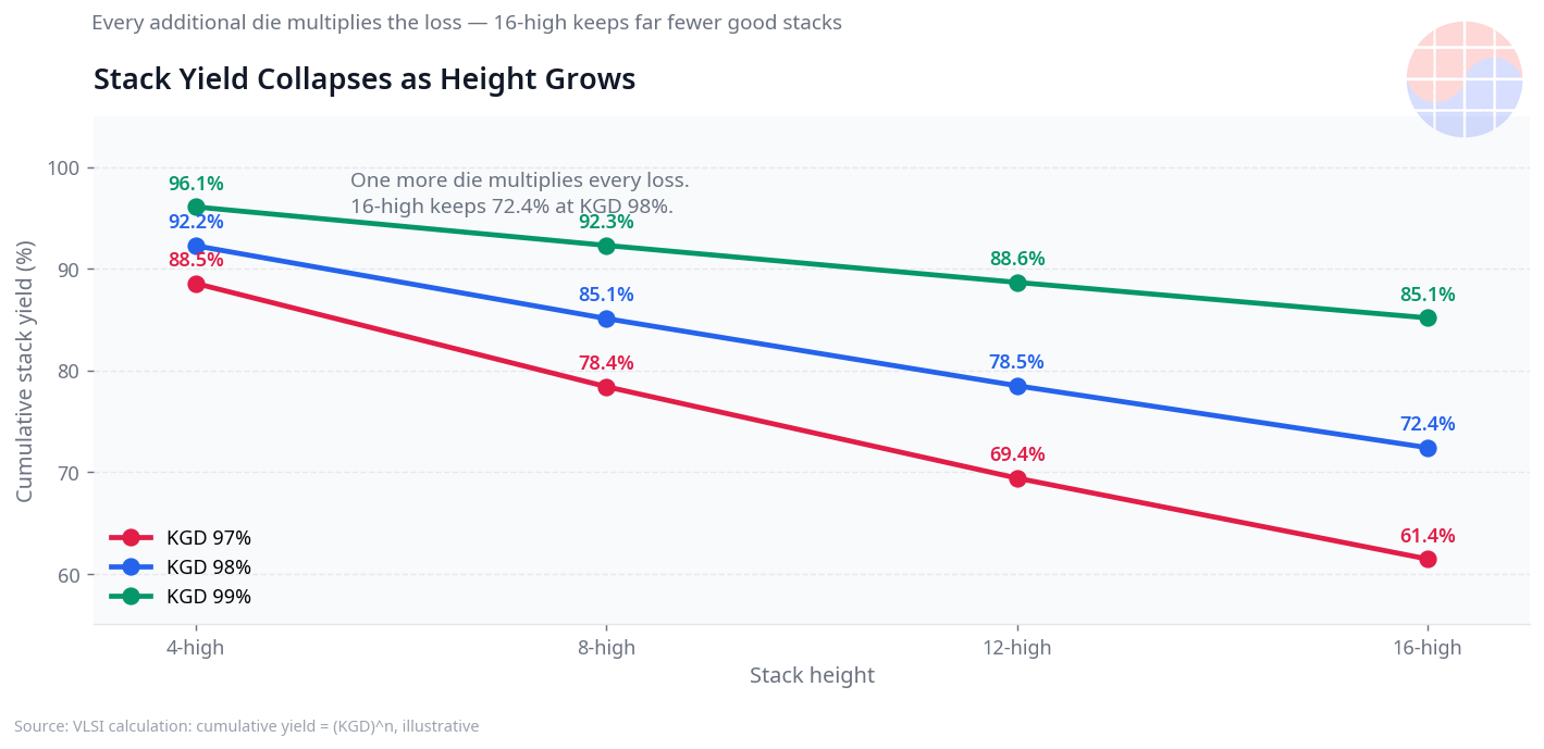
HBM pricing is, at its core, cumulative yield. If each of the N DRAM dies in a stack has a known-good-die (KGD) probability p, stack yield is p^N. At p = 98%, that is 85% for 8-high, 79% for 12-high, and 72% for 16-high. Drop die yield by a single point (p = 97%) and 16-high stack yield collapses to 62%.
Three more factors pile on. First, no rework after stacking — find a defect after all 16 dies are bonded and the whole stack is scrap. Pre-stack KGD testing is the lifeline, and test time and tester (Advantest/Teradyne-class) cost grow with height. Second, more bonding steps — die-by-die TC bonding makes height equal to takt time. Third, thinning cost — 30 µm-class thin wafers raise the difficulty of every step: handling, TSV etch (Lam, TEL tools), CMP, and metrology (KLA, Onto Innovation).
Market pricing reflects this. Industry estimates put 2027 HBM4 pricing at about USD 4.50–4.90 per Gb — nearly 3x HBM3E. Price per Gb rises with height, so the premise "if tall stacks cost the same, everyone would use them" never holds. They cannot cost the same — structurally.
Who wins — the tall-stack camp vs the short-stack camp
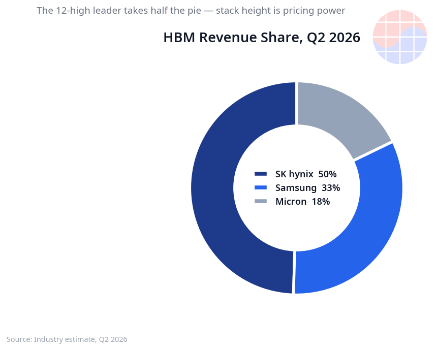
The tall-stack winners. The first mover takes the premium. In Q2 2026, SK hynix captured roughly 50% of HBM revenue, Samsung about 33%, and Micron about 18% (industry estimates) — the numbers show the payoff of ramping 12-high HBM4 first.
Samsung claims a technology lead in hybrid bonding and plays the turnkey card (memory + foundry) for what comes after 16-high. Equipment makers are on this side too: Hanmi Semiconductor, the dominant TC bonder supplier; BESI, Applied Materials, EVG, and Hanwha Semitech in hybrid bonding; Lam and TEL in TSV etch and deposition; KLA and Onto Innovation in inspection; plus advanced-packaging OSATs. Every added layer means more process steps, so the whole equipment–materials–packaging value chain benefits. Applied Materials has said its tools touch about three-quarters of HBM packaging steps and that it holds over 60% of that served market.
The short-stack winners. Paradoxically, the biggest beneficiary is NVIDIA — and the cloud vendors. With HBM wafer supply and TSMC leading-edge logic both fixed, building everything in 12-high cubes means fewer GPUs shipped. Drop to 8-high and the same wafers yield about 1.5x more stacks, while bandwidth per stack stays identical (bandwidth is set by interface width and speed, not height). Per SemiAnalysis, this rationing logic sits behind the reported Rubin Ultra spec change — from the original plan (16-high HBM4E × 16 stacks, 1 TB) to the revised one (8-high HBM4 × 8 stacks, 192 GB). There is a counter-view predicting 12-high stays (industry estimates), so treat this as reported analysis, not confirmed fact — NVIDIA has not confirmed it. Either way, short stacks are the "ship more accelerators" choice, favoring inference and cost-sensitive workloads — and followers. China's CXMT is the textbook case: 16 nm process, 8-high HBM3 ramping from roughly 25% yield, with HBM3E now in qualification. 8-high is the only zone where their economics work.
Bottleneck summary — each step dies differently
| Step | Three killer bottlenecks |
|---|---|
| 8-high → 12-high | ① Thinning DRAM to ~30 µm and thin-wafer handling breakage ② TSV etch difficulty as aspect ratio rises ③ Dependence on TSMC leading-edge logic for the base die (supply, cost) |
| 12-high → 16-high | ① Cumulative yield collapse (98% KGD → 72% stack) with no post-stack rework ② 16-high stack warpage and thermals (MR-MUF vs hybrid bonding fork) ③ Rising KGD test time and cost |
| 16-high → 20-high+ | ① Package height limit (beyond 775 µm) — hybrid bonding becomes mandatory ② Bumpless direct-bond alignment precision (~100 nm-class) and surface prep ③ HBM4E height-spec talks (~900 µm) and vendor-defined standard risk |
Outlook — 2027's three forks
Three variables decide 2027. First, HBM4E — a vendor-defined generation with no JEDEC standard as of October 2026. It keeps the 2,048-bit interface, pushes 14–16 Gbps for about 3.6 TB/s per stack, and targets 48 GB at 12-high (32 Gb dies). Samsung shipped 12-high HBM4E samples in late May, SK hynix followed about three weeks later, and Micron targets 2027 volume production. Second, the hybrid-bonding inflection — JEDEC is reportedly discussing relaxing the HBM4E height spec to around 900 µm. Relaxation extends the life of conventional TC bonders (Hanmi Semiconductor) and delays hybrid bonding (BESI, Applied Materials); a tight spec makes hybrid bonding mandatory beyond 16-high. Third, custom HBM — as Big Tech's in-house accelerators multiply, demand for customer-specific stacks beyond standard HBM is growing. The stack-height debate ultimately converges on one question: who buys memory, for which workload, at what price. Stack height is not a spec — it is a price tag.
Market-share, pricing, and yield figures are industry estimates as of October 2026. The Rubin Ultra specification change is at the reported-analysis stage and has not been confirmed by NVIDIA. HBM capacity is stated in Gb.