VLSI Korea
Hyper NA EUV: ASML and Zeiss's 10-Year Blueprint Beyond High NA (Deep Dive)
In a peer-reviewed paper, engineers from ASML and Carl Zeiss SMT have published the first system-level blueprint for "Hyper NA" EUV lithography — NA of at least 0.75, targeting 5nm-class features on the same 13.5nm wavelength. The mirrors are ready and the light source can be reused. What remains: polarization, mask 3D effects, mechanical


In a peer-reviewed paper, engineers from ASML and Carl Zeiss SMT have published the first system-level blueprint for "Hyper NA" EUV lithography — NA of at least 0.75, targeting 5nm-class features on the same 13.5nm wavelength. The mirrors are ready and the light source can be reused. What remains: polarization, mask 3D effects, mechanical stability, and economics.
30-Second Summary (TL;DR)
- What happened: The October 2026 issue of the Journal of Micro/Nanopatterning, Materials, and Metrology carries "Hyper-NA: a system with a numerical aperture of at least 0.75" by Patra, Michael (Zeiss), Feldmann, Neumann, and Bottiglieri (ASML) — the first peer-reviewed system paper on the successor to High NA EUV (0.55 NA). Source
- Key specs: Keep the 13.5nm wavelength, raise NA from 0.55 to 0.75 or higher, targeting 5nm-class features — more than a third smaller than High NA's 8nm. Source
- Readiness: Zeiss can already manufacture mirrors precise enough for Hyper NA, and the existing EUV light source "can be reused as is." The tool would be barely larger than High NA systems. Source
- Timeline and caveats: The engineers see readiness in about 10 years, but ASML has begun development without committing to production. Remaining challenges: polarization, reticle 3D effects, mechanical stability, and customer demand/economics. Source
Background: DUV 193i → EUV 0.33 NA → High NA 0.55 NA
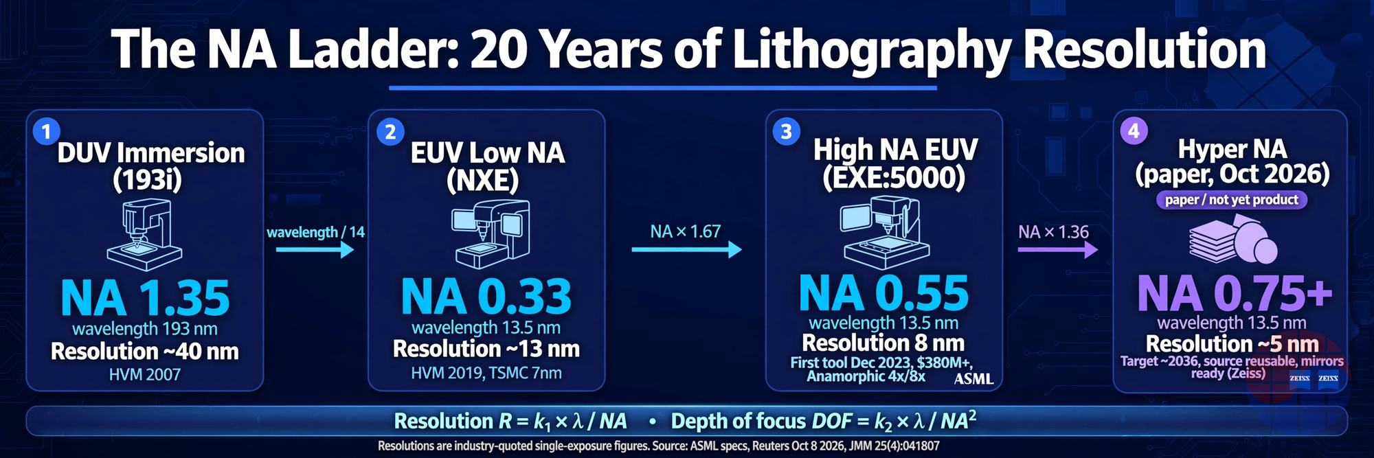
The history of lithography is a loop of "shorter wavelength, larger NA." The physics of resolution (Rayleigh criterion) is simple: R = k1 · λ / NA. Shrink the wavelength λ, widen the light-gathering angle (NA), or push the process factor k1 lower — those are the only three levers.
The DUV 193i era: Water immersion (2007) pushed NA to 1.35. But with wavelength fixed at 193nm, single-exposure resolution hit a wall around 40nm. The industry survived on double and quadruple patterning (SADP/SAQP), at the cost of exploding mask counts, process steps, and overlay risk. Below 10nm-class logic, DUV multi-patterning hit its economic limit.
The EUV 0.33 NA era: The gambit was cutting wavelength 14× to 13.5nm. Starting with TSMC 7nm volume production in 2019, the 5nm and 3nm nodes were built on EUV single exposure (~13nm resolution). The price was steep: no refractive lenses allowed, so an entirely new system — all-reflective Mo/Si multilayer mirror optics, vacuum, reflective masks — plus a decade-long fight over source power and resists.
The High NA 0.55 NA era: Same wavelength, NA raised from 0.33 to 0.55. ASML's TWINSCAN EXE:5000/5200B is specified at 8nm resolution, ~40% higher imaging contrast than NXE, ~1.7× smaller features per exposure and up to 2.9× transistor density. Source The key trick is anamorphic optics: a bigger NA needs a bigger optical column that would exceed the 6-inch reticle standard, so the projection optics demagnify 4× in one axis and 8× in the other, keeping mask size constant. The cost: exposure field halved (26 × 16.5mm), $380–400M per tool, and a footprint the size of a double-decker bus. Source
Adoption speed diverges sharply by vendor. Intel is the most aggressive — High NA is already in production on select Panther Lake (18A) layers, with over 1.35 million wafers processed across development and volume. Source Samsung and SK hynix have committed to 2028, TSMC to 2030. Source That gap is the key variable setting Hyper NA's commercial timeline.
Deep Dive: The Physics and Engineering of Hyper NA
1. How much resolution does NA 0.75 buy?
Plug λ = 13.5nm into R = k1 · λ / NA with k1 = 0.4 (representative of aggressive single exposure):
| System | NA | R (k1=0.4) | Industry-quoted resolution |
|---|---|---|---|
| EUV (NXE) | 0.33 | ~16.4nm | ~13nm |
| High NA (EXE) | 0.55 | ~9.8nm | 8nm |
| Hyper NA | 0.75 | ~7.2nm | ~5nm (paper) |
NA ratio alone gives 0.55 → 0.75 = 1.36× resolution improvement. But the paper's 8nm → 5nm is 1.6×. The difference sits in k1: the 5nm target assumes a lower k1 — better resists (lower LER at dose), source-mask optimization (SMO), and advanced RET progressing in parallel. Reuters' "more than a third smaller" comes from this 5nm-vs-8nm comparison. To be physically honest: NA scaling delivers 1.36×; the rest depends on the ecosystem doing its homework.
2. DOF collapse: the real price of bigger NA
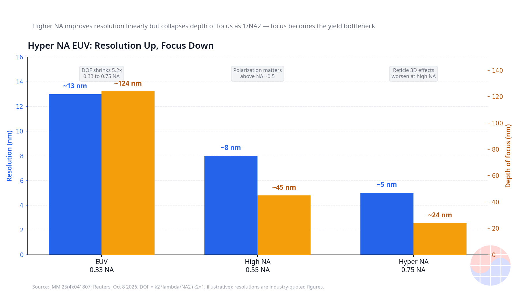
Resolution's twin is depth of focus: DOF = k2 · λ / NA². NA sits in the denominator squared, so focus latitude collapses fast. With k2 = 1:
- 0.33 NA: ~124nm
- 0.55 NA: ~45nm
- 0.75 NA: ~24nm
Going 0.33 → 0.75 shrinks DOF 5.2×. The practical meaning of 24nm is brutal: wafer topography, resist thickness, chuck flatness, and focus control errors must all fit inside a ~20nm budget combined. Focus budgets were already tight at High NA; at Hyper NA, focus threatens to become the first-order yield limiter. That is why the paper treats system stability alongside optical architecture. Research on a Hyper NA micro-exposure tool (MET) estimates the 0.55 → 0.75 NA step demands a 3× improvement in mechanical stability, targeting ~0.35nm rms image stability on-wafer during exposure. Source A MET is not an HVM scanner, but the direction of the stability requirement is the same.
3. Anamorphic optics extended — and reticle 3D effects
High NA's 4×/8× anamorphic demagnification will likely carry over: an isotropic 4× design at 0.75 NA would make the mirrors unmanageably large. But this choice worsens reticle 3D effects (mask shadowing). EUV masks are reflective, so light arrives at oblique incidence; larger NA means larger incidence angles and longer absorber shadows. Asymmetric shadowing in X vs. Y creates H-V bias that lands squarely on the OPC model. The paper's decision to cover reticle 3D effects as a standalone topic signals that how much of the resolution gain survives the mask is central to commercial viability.
4. Polarization: the vector-imaging problem that starts at 0.55
Above NA ~0.5, the scalar diffraction approximation breaks down and polarization starts eating contrast. Imec's Kurt Ronse has already flagged that "light polarization becomes a problem starting around 0.55 NA." Source At 0.75, polarization control is mandatory, not optional — illumination optics must control polarization state sector by sector, as MET research confirms. Source That is why polarization is one of the paper's four pillars.
5. Two problems already solved: mirrors and source
The most strategic message of the paper: Zeiss can already make mirrors precise enough for Hyper NA, and the current EUV source can be reused as-is. The two mountains that made EUV and High NA each take a decade — the projection optics and the light source — are declared climbed. Recall that more than half of High NA's long development was the fight over Zeiss's anamorphic optics and source power; the weight of this claim is tangible. That the tool would be "barely larger" than High NA also matters for fabs — customers who suffered through fab layout, crane, and vibration specs for High NA are told "it fits the same slot, with the same source," lowering the adoption barrier.
There is nuance in the source-reuse claim. The paper notes that a free electron laser (FEL) alternative would not change the illuminator design. Source Read it as insurance: with Elon Musk evaluating FEL sources for Terafab ("FEL FTW") and startups like xLight (chaired by Pat Gelsinger, $150M CHIPS Act award in June 2026, prototype targeted 2028) pushing source-replacement scenarios, ASML and Zeiss are preemptively stating "whatever the source, our optical architecture stands." Source
6. Fact-checking the "about 10 years" claim
How credible is "ready in about 10 years"? Cross-check:
- Precedent: High NA took roughly a decade from mid-2010s concept discussions to first shipment (December 2023, Intel Oregon) and HVM entry (2024–2026). EUV 0.33 NA took 10+ years from early alpha tools to 2019 HVM. Lithography generation turnover runs on a physical ~10-year cadence.
- What's shifted: In May 2024, then-ASML president Martin van den Brink first put Hyper NA (0.75 NA) on the roadmap at imec's ITF World, pointing at ~2030. Source The 2026 paper's "about 10 years" points at ~2036 — six years of slip in two years, consistent with ASML walking its official stance back to "feasibility studies are ongoing" (ASML's clarification to EE Times in 2024). Technical readiness and the production decision are decoupling.
- Counterpoint: Ten years is an engineering estimate premised on "mirrors and source are ready." The real schedule is held by customer pull. If TSMC adopts High NA in 2030, Hyper NA volume demand lands in the mid-to-late 2030s. No vendor builds a $400M+ tool (High NA pricing; Hyper NA would exceed it) without customer commitments — which is exactly why ASML says development has started but production is uncommitted.
Bottom line: ten years is reasonable as an engineering schedule with optics and source de-risked, but the commercial date is hostage to how fast TSMC and Samsung digest High NA.
7. Which node needs 5nm-class features?
5nm half-pitch corresponds to ~10nm-class metal pitch — the critical layers of sub-2nm logic (beyond Intel 14A; A14/A10-class at TSMC) and periphery/storage-node patterns of sub-10nm-class DRAM (post-1b generations). In other words, Hyper NA does not target "beyond 2nm" — it targets the 1nm-class regime where even High NA single exposure starts to struggle. If High NA is the tool that removes multi-patterning for 2nm-class logic, Hyper NA plays the same role one generation later.
Chase's Take: What "Lithography Is a Limiting Factor" Means in Practice
Having done STA signoff in PrimeTime and physical design tapeouts, the sentence "lithography is a limiting factor" lands differently — it shows up in numbers I look at daily.
First, the standard-cell architecture ceiling is lithography. Shrinking cell height (track count) means shrinking contacted poly pitch (CPP) and metal pitch (MMP), and both are set directly by lithography resolution. Just as High NA's 8nm enabled 2nm-class cells, Hyper NA's 5nm is the precondition for the next cell library generation. DTCO can be brilliant, but it cannot optimize a pitch that cannot be printed. "We compensate with 3D" (GAA, CFET, backside power) is transistor-structure innovation, not interconnect-pitch innovation. If BEOL doesn't shrink, cell area doesn't shrink.
Second, PPA's center of gravity is already in BEOL. Below 3nm, wire RC dominates timing over cell delay — every signoff engineer knows this. Tighter single-exposure metal pitch from Hyper NA means shorter wires at the same drive strength, less coupling capacitance — direct wins in dynamic power and IR drop. Conversely, DOF collapse (24nm) degrading LER and CD uniformity forces larger on-chip variation (OCV) derates and fatter STA margins. A practitioner's instinct: part of the resolution gain gets handed back as variation penalty.
Third, from an EDA standpoint this is good news. Multi-patterning is a complexity disaster for EDA: coloring for double patterning, cut masks, stitching-aware routing, multi-patterning-aware DRC — all of it shrinks or vanishes in front of Hyper NA single exposure. Like High NA before it, Hyper NA both "prints more" and "asks tools to worry about less." The remaining homework — reticle 3D effects and H-V bias — stays with OPC and litho modeling. For EDA vendors, the money migrates from litho simulation toward P&R.
Fourth, the Korea timing risk. Samsung Foundry and SK hynix adopt High NA in 2028, TSMC in 2030. If Hyper NA opens in the mid-2030s, late High NA adopters face "buy Hyper NA before High NA depreciation is done" capex pressure. Samsung Foundry, already fighting the 2nm yield and order battle, gets another capex-timing tangle. On memory, the business case for Hyper NA hinges on how many EUV layers SK hynix's and Samsung's HBM/DRAM roadmaps actually use.
Implications
ASML's moat extends by a decade. The moat is Zeiss. ASML bought 24.9% of Carl Zeiss SMT for €1B in 2016 plus ~€760M in R&D/capex support. Source Zeiss is the only company on Earth that can build EUV projection optics, and now its engineers say Hyper NA mirrors are already manufacturable. The optics barrier is ASML's moat. Nikon and Canon are stuck in DUV; challengers must replace the entire architecture.
The challengers' angles: Substrate (X-ray lithography, $1B valuation in October 2025, foundry-service model) and xLight (FEL source, Gelsinger as chair) are the notable ones. Source The paper's FEL footnote — "would not change the illuminator design" — reads as a preemptive message to them: even if the source changes, the optics stay ours.
Value chain: The source-reuse declaration matters for the supply chain too. Trumpf (CO₂ lasers), the Cymer source stack, and the whole EUV ecosystem stay valid into Hyper NA — extending everyone's investment payback period. "Extending the existing EUV ecosystem" is the paper's literal theme. Source
Beyond Hyper NA: The authors see shorter wavelengths next — the 6.x nm band ("BEUV") is still academic research. In other words, the 13.5nm wavelength's physical lifetime runs through Hyper NA: the wavelength isn't changing before the 2040s.
One-line investment read: For ASML, Hyper NA is "the growth story after High NA." Putting the next generation's technical feasibility into peer review just as High NA's HVM ramp (2025–2030) plays out serves customer capex persuasion and capital-markets storytelling at once. With production uncommitted, it's not near-term numbers material.
FAQ
What exactly is Hyper NA's numerical aperture?
Per the paper's title: "at least 0.75" — 0.75 or higher, one step above High NA's 0.55. The unspecified upper bound leaves room for optical design trade-offs (mirror size, polarization, DOF) to push beyond 0.75. Source
What changes versus High NA?
Same 13.5nm wavelength; only NA rises, 0.55 → 0.75+. Industry-quoted resolution moves 8nm → 5nm-class. The NA step itself gives 1.36×; reaching 5nm additionally requires resist, RET, and illumination improvements (lower k1). The tool stays nearly the same size as High NA and reuses the light source, per the paper. Source
When will volume tools appear?
The authors see ~10 years (mid-2030s), but ASML has not committed to production. The real date depends on how fast customers digest High NA — TSMC plans 2030, Samsung/SK hynix 2028 — and on customer commitments for a tool priced above $400M. Source
Can the existing EUV source really be reused as-is?
The paper states it "can be reused as is" — meaning the optical and illuminator architecture is compatible with current sources. Dose/throughput still need the source power roadmap to keep climbing, and the paper's footnote adds that even an FEL alternative wouldn't change the illuminator design. Source
This analysis is based on the published paper (abstract and press coverage); the full text sits behind the SPIE Digital Library paywall, so detailed figures were cross-verified against secondary sources. Quoted resolutions and timelines reflect reporting as of October 8–9, 2026 and are not ASML's official production plans.