VLSI Korea
NVIDIA Vera CPU Deep Dive: Why 1.2 TB/s of Memory Bandwidth Matters More Than 88 Cores
Vera delivers 1.5 TB of SOCAMM2 LPDDR5X and 1.2 TB/s per socket, about 13.6 GB/s per core. A full comparison with Grace and EPYC Turin, plus the limits of vendor claims and the SOCAMM2 memory race.


NVIDIA Vera CPU Deep Dive: Why 1.2 TB/s of Memory Bandwidth Matters More Than 88 Cores
TL;DR
- NVIDIA Vera is an 88-core data center CPU built on custom Olympus cores compatible with Armv9.2-A, first unveiled with the Vera Rubin platform at GTC in March 2025, with detailed architecture disclosures following in July 2026 (NVIDIA architecture disclosure, July 2026).
- The headline number is not the core count. Each Vera socket supports up to 1.5 TB of SOCAMM2 LPDDR5X memory and up to 1.2 TB/s of memory bandwidth, roughly 13.6 GB/s per core by simple division (NVIDIA architecture disclosure, July 2026; calculation from disclosed figures, October 20, 2026).
- That per-core bandwidth is about 1.8 times the figure for the prior Grace CPU and about 2.8 times a calculated figure for a 128-core AMD EPYC Turin flagship using 12-channel DDR5-6400 (calculation from vendor specifications, October 20, 2026).
- NVIDIA claims up to 1.9x instructions per cycle versus EPYC Turin in AI-related workloads, but that is a vendor claim, and the partner benchmark results published so far do not disclose full configuration or TDP settings (NVIDIA disclosure, July 2026).
- The strategic shift is memory content per socket: Vera carries 3 times the memory capacity of Grace per socket, which turns the CPU socket into a contest for LPDDR5X supply among Samsung Electronics, SK hynix, and Micron (NVIDIA architecture disclosure, July 2026).
Background
For two decades, data center CPU marketing was mostly a core-count race. That logic worked while general-purpose workloads were limited mainly by compute throughput. It works less well in the era of agentic AI, where the CPU is no longer a passive host for GPUs. It orchestrates tool calls, prepares and moves data, runs retrieval and ranking, handles networking and storage traffic, and feeds accelerators that stall quickly when data arrives late.
NVIDIA entered this market with Grace, a 72-core Arm Neoverse V2 CPU with up to 480 GB of LPDDR5X and 546 GB/s of bandwidth (NVIDIA Grace specifications, disclosed before July 2026). Grace proved an Arm CPU could sit at the center of an NVIDIA rack — and exposed the next constraint: faster GPU systems need more host memory capacity, more bandwidth per thread, and a faster coherent link.
Vera is NVIDIA's answer, unveiled as part of the Vera Rubin platform at GTC in March 2025 and detailed in architecture disclosures in July 2026 (GTC, March 2025; NVIDIA architecture disclosure, July 2026). Vera replaces the licensed Neoverse design with 88 custom Olympus cores. NVIDIA reports Spatial Multithreading that exposes 176 threads, a monolithic compute die, 2 MB of L2 cache per core, 164 MB of L3 cache, and a second-generation Scalable Coherency Fabric (NVIDIA architecture disclosure, July 2026).
Vera also provides NVLink-C2C at 1.8 TB/s for coherent CPU-to-GPU communication, PCIe Gen6, and CXL 3.1, with a configurable TDP of 250 to 450 W (NVIDIA architecture disclosure, July 2026). Two Vera CPUs form a Superchip with 176 cores, 352 threads, 16 SOCAMM2 modules, 2.4 TB/s of memory bandwidth, and 3 TB of memory; a rack reference with 128 Superchips reaches 22,528 cores and 384 TB (NVIDIA architecture disclosure, July 2026). Standalone CPU sales and initial customer shipments were reported during 2026, so availability here is stated on a reported basis (industry reporting, 2026).
Deep Dive 1: The Memory System — 1.5 TB and 1.2 TB/s per Socket
Vera's defining choice is its memory system. Each socket supports up to 1.5 TB of SOCAMM2 LPDDR5X at speeds up to 9,600 MT/s, delivering up to 1.2 TB/s of memory bandwidth (NVIDIA architecture disclosure, July 2026). SOCAMM2 is a socketed LPDDR module standard championed by NVIDIA. Unlike soldered LPDDR, a socketed module can be configured, serviced, and scaled per system design, while keeping the power efficiency advantages of LPDDR5X over conventional DDR5 server memory.
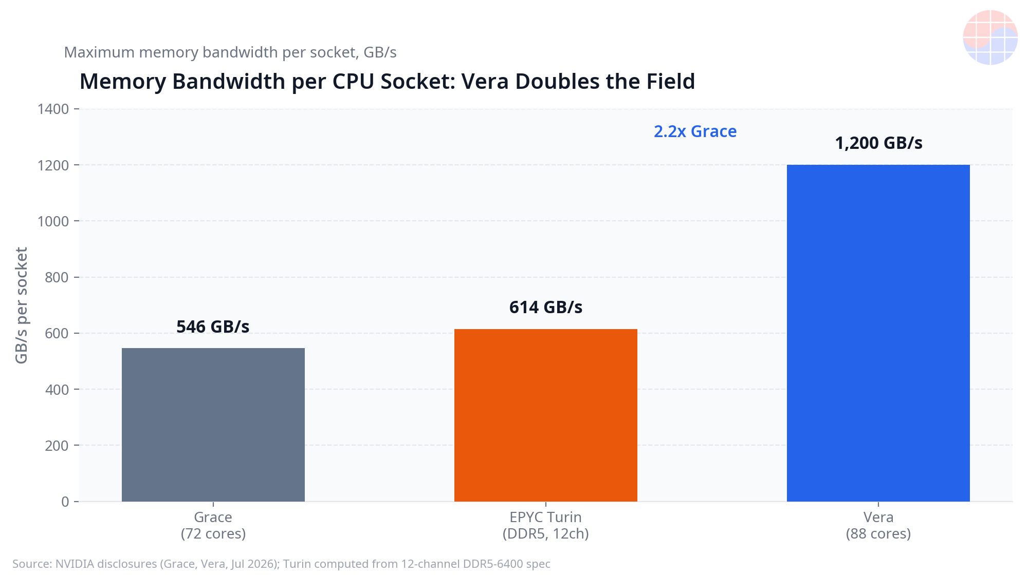
The comparison with Grace shows how far the design moved in one generation. Grace offered up to 480 GB of LPDDR5X and 546 GB/s of bandwidth per socket (NVIDIA Grace specifications). Vera triples the capacity to 1.5 TB and raises bandwidth to 1,200 GB/s, a 2.2 times increase (NVIDIA architecture disclosure, July 2026; calculation, October 20, 2026). In practical terms, a Vera socket holds larger working sets locally: bigger key-value caches, larger embedding tables, more concurrent agent sessions, and more data staged for the GPU.
Capacity and bandwidth must rise together: capacity without bandwidth leaves cores waiting, and bandwidth without capacity forces frequent eviction and refetch. Vera's design point — 1.5 TB at 1.2 TB/s — targets workloads where many threads touch large, changing data sets at once: retrieval pipelines, feature serving, vector search preprocessing, data loading, and control logic around large model inference.
A socketed LPDDR5X standard also creates a defined, replaceable unit of memory content bought in volume. At 1.5 TB per socket instead of 480 GB, every Vera system multiplies the LPDDR5X content attached to the CPU, before any HBM on the GPU is counted — a point Section 4 revisits for Samsung Electronics, SK hynix, and Micron.
Deep Dive 2: Per-Core Bandwidth and the x86 Comparison
Core counts mislead when memory bandwidth does not keep pace. Dividing socket bandwidth by core count gives a rough but useful measure of how much memory throughput each core can draw when all cores are busy. For Vera, 1,200 GB/s divided by 88 cores is about 13.6 GB/s per core, which NVIDIA rounds to about 14 GB/s per core (NVIDIA architecture disclosure, July 2026; calculation, October 20, 2026). For Grace, 546 GB/s divided by 72 cores is about 7.6 GB/s per core.
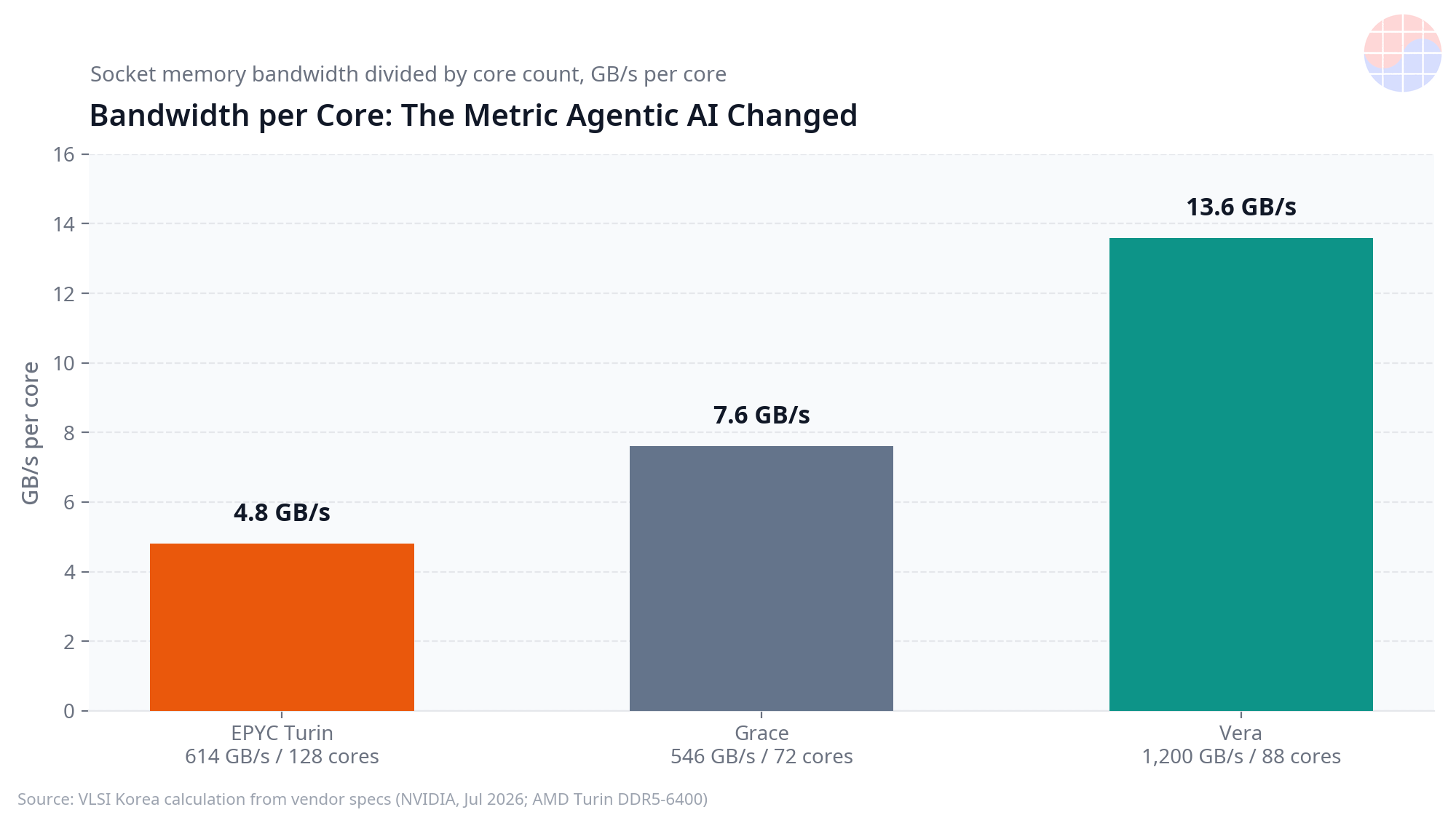
The x86 comparison requires a transparent method. An AMD EPYC Turin system with 12 channels of DDR5-6400 has a theoretical peak of 614 GB/s, calculated as 12 channels multiplied by 6,400 MT/s multiplied by 8 bytes per transfer (calculation from AMD EPYC Turin memory specifications, October 20, 2026). Spread across a 128-core flagship configuration, that is about 4.8 GB/s per core. Real sustained bandwidth is lower than theoretical peak for every platform in this comparison, so the figures should be read as specification-based ratios, not as measured application results.
On that basis, Vera offers roughly 2.8 times the per-core bandwidth of the Turin configuration and roughly 1.8 times that of Grace (calculation, October 20, 2026). This is the strongest part of NVIDIA's argument. Agentic and data-heavy workloads often run many threads that each stream, filter, or transform data. When per-core bandwidth is low, adding cores stops helping because the cores share a fixed memory pipe. When per-core bandwidth is high, thread scaling lasts longer.
NVIDIA also claims up to 1.9x instructions per cycle versus EPYC Turin in AI-related workloads (vendor claim, NVIDIA disclosure, July 2026). Treat it carefully: IPC depends on workload, compiler, and instruction mix, and Arm and x86 cores do not execute identical instruction streams. It signals design intent, not an independent measurement; buyers should wait for reproducible benchmarks with disclosed configurations.
Deep Dive 3: Olympus Cores, Coherency, and the Superchip
Vera's 88 Olympus cores are custom designs compatible with Armv9.2-A, beyond Grace's licensed Neoverse V2 cores (NVIDIA architecture disclosure, July 2026). Owning the design lets NVIDIA tune vector throughput and cache hierarchy for its rack workloads. Each core carries 2 MB of L2 cache and the chip 164 MB of L3, reducing how often threads wait on main memory (NVIDIA architecture disclosure, July 2026).
Spatial Multithreading doubles the exposed thread count to 176 threads per socket (NVIDIA architecture disclosure, July 2026). Thread doubling only pays off if the memory system can feed the extra threads, which is why the 1.2 TB/s figure and the thread count should be read as one design decision, not two separate specifications.
Coherency is the second pillar. The second-generation Scalable Coherency Fabric and NVLink-C2C at 1.8 TB/s let CPU and GPU share data coherently far above PCIe speeds, while PCIe Gen6 and CXL 3.1 attach conventional accelerators, network adapters, and memory expansion (NVIDIA architecture disclosure, July 2026). Coherent sharing reduces copy overhead: the CPU can prepare data structures the GPU consumes directly.
The Superchip scales the same idea: two Vera CPUs deliver 176 cores, 352 threads, 2.4 TB/s, and 3 TB across 16 SOCAMM2 modules, and the rack reference totals 22,528 cores and 384 TB across 128 Superchips — a CPU layer designed as pooled infrastructure for agent fleets, not a minimal GPU host (NVIDIA architecture disclosure, July 2026).
Power is configurable between 250 W and 450 W TDP (NVIDIA architecture disclosure, July 2026). That range matters for interpretation of any benchmark: a result at 450 W and a result at 250 W describe different operating points, and comparisons that do not state the setting are incomplete.
Deep Dive 4: The Honest Limits — Benchmarks, x86 Response, and Monolithic Cost
Three limits deserve direct attention. First, the public benchmark evidence is thin. Partner results, including streaming data results associated with Redpanda, were published without full disclosure of configuration and TDP settings (partner benchmark publications, 2026). Without core counts at test time, memory population, firmware, and power settings, outside readers cannot reproduce the numbers or judge whether the comparison was fair. NVIDIA's up to 1.9x IPC claim carries the same status: it is a vendor claim until independent testing with disclosed methods confirms it (NVIDIA disclosure, July 2026).
Second, x86 vendors are not standing still. Faster DDR5, MRDIMM memory that raises effective bandwidth per channel, and new generations with more channels will narrow the per-core bandwidth gap from the 614 GB/s baseline above. Vera's lead is real on specifications disclosed as of October 20, 2026, but it is a lead at a point in time, not a permanent structural gap.
Third, Vera's monolithic compute die has a cost profile. A large monolithic die generally faces harder yield economics than a chiplet design that discards only a small defective die and reuses known good dies across products (general semiconductor manufacturing principle, stated October 20, 2026). NVIDIA has not disclosed Vera yield or unit cost, so no specific cost claim is made here; the point is directional — the choice that helps latency and coherency also concentrates manufacturing risk.
Finally, software decides how much of the hardware advantage survives production. Arm tooling and middleware have improved, but migration remains a real cost for large x86 estates. Bandwidth wins benchmarks; total cost of ownership wins purchase orders.
Chase's Take
The important shift is not that NVIDIA built an 88-core CPU; it is where the bottleneck moved. In agentic AI systems, the CPU handles orchestration: planning loops, tool invocation, retrieval, memory management for long contexts, and data movement between storage, network, and GPU. Those tasks are thread-rich and memory-hungry, and their limiting resource is rarely peak floating-point throughput — it is how much data each thread can reach, how fast, without queueing behind every other thread. Vera is designed around that reality: bandwidth per core and capacity per socket first, core count second.
From a business perspective, SOCAMM2 may matter even more than the Olympus core. By defining a socketed LPDDR5X module, NVIDIA turned host memory into a standardized, high-volume content slot: 1.5 TB per socket against Grace's 480 GB, three times the content per socket (NVIDIA architecture disclosure, July 2026).
That makes the CPU socket a memory-content battleground. Samsung Electronics, SK hynix, and Micron compete in LPDDR5X supply, and qualification for a high-volume NVIDIA platform anchors volume, pricing power, and a position in the next module revision. Korean suppliers have a particular stake: LPDDR leadership has historically been a Korean strength, and SOCAMM2 gives it a new server-side outlet beyond smartphones. Read from Seoul, the Vera story is partly about who sells the memory that surrounds the CPU.
My judgment: judge Vera on per-core bandwidth delivered in production agent workloads, not on the 88-core headline or undisclosed benchmark settings. If independent tests confirm even most of the specification advantage, pressure on x86 roadmaps — more channels, MRDIMM adoption, lower core counts per bandwidth tier — will be the clearest sign Vera changed the market.
Implications
- For AI system buyers: Evaluate Vera on bandwidth per core and memory capacity per socket for your own agent, retrieval, and data-loading workloads, and require disclosed TDP and memory configuration in every vendor benchmark (basis: NVIDIA architecture disclosure, July 2026).
- For x86 platform planning: The specification gap — about 13.6 GB/s per core for Vera versus about 4.8 GB/s per core for a 128-core Turin configuration with DDR5-6400 — makes MRDIMM and higher-channel designs a roadmap priority, not an option (calculation, October 20, 2026).
- For memory suppliers: SOCAMM2 raises CPU-side LPDDR5X content to 1.5 TB per socket, three times Grace, so Samsung Electronics, SK hynix, and Micron are competing for a larger and more strategic socket (NVIDIA architecture disclosure, July 2026).
- For operators: Migration cost, software ecosystem fit, and monolithic-die pricing may offset part of the hardware advantage; total cost of ownership testing matters more than headline IPC claims.
- For the CPU market: If agentic workloads keep growing, per-core bandwidth becomes a first-order purchase criterion alongside core count, and CPU marketing that leads with cores alone will age badly.
This article is based on NVIDIA disclosures dated March 2025 and July 2026 and on specification calculations dated October 20, 2026; vendor performance claims are labeled as such and have not been independently verified.
FAQ
Q1. What is the NVIDIA Vera CPU and when was it disclosed? Vera is NVIDIA's data center CPU with 88 custom Olympus cores compatible with Armv9.2-A and 176 threads via Spatial Multithreading. It was unveiled with the Vera Rubin platform at GTC in March 2025, and NVIDIA published detailed architecture disclosures in July 2026.
Q2. How much memory bandwidth and capacity does Vera provide per socket? Each Vera socket supports up to 1.5 TB of SOCAMM2 LPDDR5X at up to 9,600 MT/s and up to 1.2 TB/s of memory bandwidth, which is about 13.6 GB/s per core across 88 cores (NVIDIA architecture disclosure, July 2026).
Q3. How does Vera compare with Grace and AMD EPYC Turin on bandwidth per core? Grace provides 546 GB/s across 72 cores, or about 7.6 GB/s per core. A 128-core EPYC Turin configuration with 12-channel DDR5-6400 has a theoretical 614 GB/s, or about 4.8 GB/s per core. Vera's roughly 13.6 GB/s per core is about 1.8 times Grace and about 2.8 times that Turin configuration, on a specification basis (calculation, October 20, 2026).
Q4. What are the main limits and open questions for Vera? NVIDIA's up to 1.9x IPC claim versus Turin is a vendor claim, partner benchmarks such as the Redpanda results do not disclose full configuration or TDP settings, x86 platforms are responding with MRDIMM and next-generation memory designs, and Vera's monolithic die may carry higher manufacturing cost than chiplet alternatives. Independent benchmarks with disclosed methods are still needed (status as of October 20, 2026).
📩 Subscribe to VLSI Korea
Get our daily semiconductor deep-dives delivered to your inbox first. Free to subscribe.