VLSI Korea
Samsung's 42nm 3D Stacked FET: Inside the VLSI Symposium Best Paper
A deep technical dive into Samsung's Best Paper at the 2026 VLSI Symposium: the world's first 3D stacked FET for logic at 42nm gate pitch, the RBC vertical interconnect, triple nanosheets, and where theory meets reality.


⏱ 30-second summary
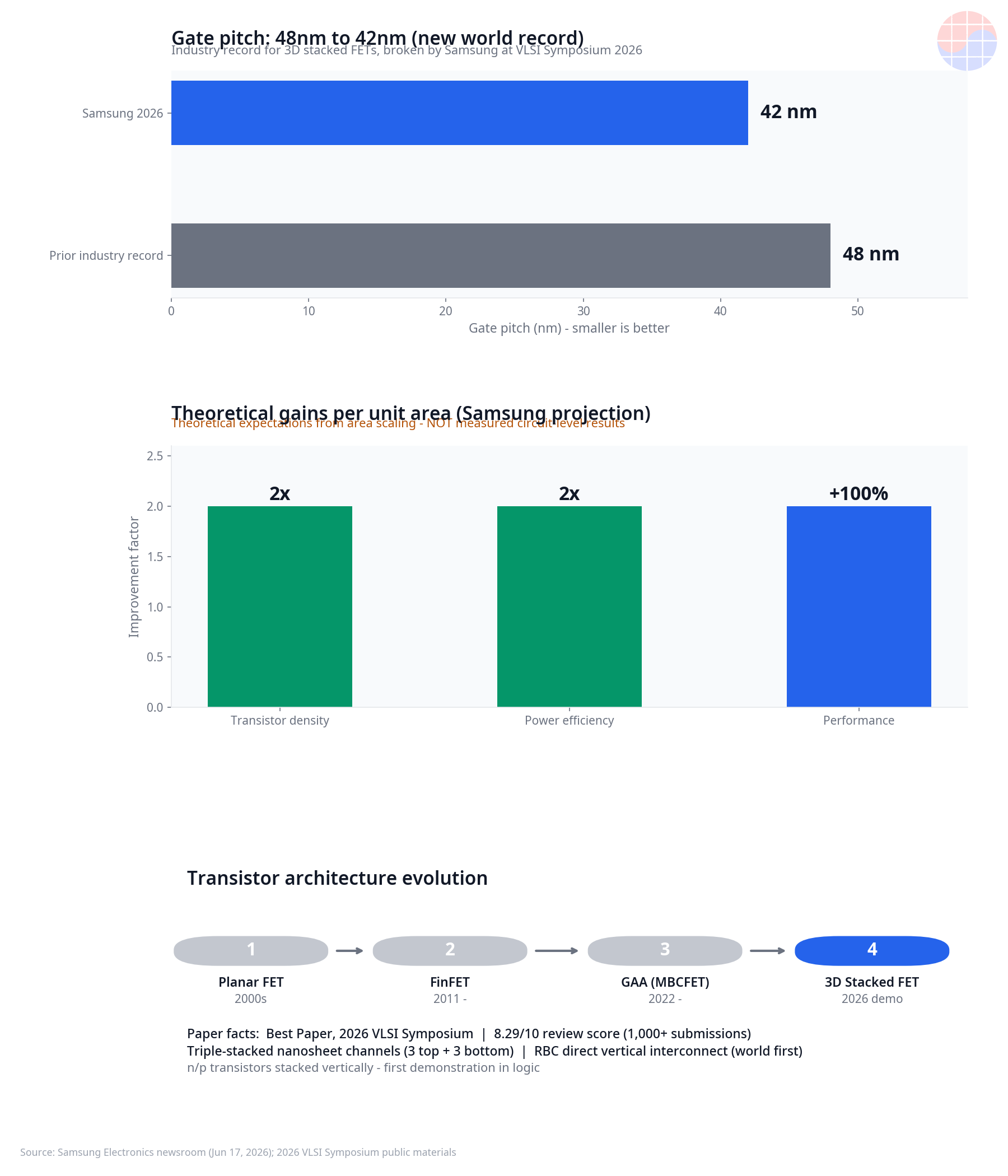
Samsung Electronics' Semiconductor R&D Center (Logic TD team) demonstrated the world's first 3D Stacked FET for logic at a 42nm gate pitch, winning Best Paper at the 2026 VLSI Symposium (top score among 1,000+ submissions, 8.29/10). The breakthroughs: vertically stacked n/p transistors with triple-stacked nanosheet channels on each tier, connected by the world's first direct vertical interconnect, RBC (RX Bounded Contact). Theory promises 2x density, 2x power efficiency, and +100% performance per area — but this is a device-level demo; logic-circuit implementation and manufacturing validation are still ahead.
Why open the series with this paper
Three reasons. First, it is a structural inflection point: the first demonstration of vertical transistor stacking — previously a memory-only trick — in logic, attacking the physical limits of planar scaling from the vertical axis. Second, the details are public: gate pitch, nanosheet stack count, interconnect architecture, and even the review score were disclosed through Samsung's official announcement, so this analysis can be evidence-based rather than speculative. Third, it connects to the reader's daily work: thermal, power-delivery, and PDK-modeling challenges of 3D-stacked devices land squarely in STA/signoff territory, and the foundry-competition angle gives the MBA lens plenty to chew on.
Background: where planar scaling stopped
The history of Moore's law is a history of transistor architecture. Planar FET gave way to FinFET, then to Gate-All-Around (GAA) — each step wrapping the gate more completely around the channel to choke off leakage. Samsung was first to ship GAA (MBCFET) in 3nm production.
But shrinking pitch on a flat plane hit a physical wall. As transistors are packed tighter, the insulator separating them gets thinner; below a critical thickness it stops insulating, current leaks, and devices malfunction. Horizontal density scaling effectively has a ceiling.
Memory showed the way out. V-NAND in flash and HBM in DRAM already broke density limits by stacking vertically instead of shrinking laterally. Logic had the same idea on paper for years: the CFET (Complementary FET) concept stacks n-type and p-type transistors on top of each other. Simple on a whiteboard, brutal in a fab — power delivery to two tiers, manufacturing uniformity, and electrical interference between stacked devices blocked real demonstrations. This paper is the first complete demo that works through all three.
What the paper actually showed
1. Device structure: stacked n/p, triple nanosheets per tier
The paper — "First Demonstration of 3D Stacked FETs at Gate Pitch of 42nm Featuring Triple-Stacked Nanosheet Channels for Advanced Logic Applications" — has two structural pillars. First, n-type and p-type transistors, conventionally placed side by side, are stacked vertically. Second, each tier carries triple-stacked nanosheet channels, widening the current path enough to deliver sufficient drive current in an extremely compact structure. Three sheets per tier is the world-leading level for this device class.
2. 42nm gate pitch: a new industry record
Gate pitch — the center-to-center distance between adjacent gates — was reduced from the previous industry record of 48nm to 42nm, the smallest ever reported for this kind of device. (For context, Samsung previously demoed a 3DSFET at 45nm CPP at IEDM 2023; the 42nm result is the follow-up peak.) This record was a direct input to the Best Paper selection.
3. RBC: the world's first direct vertical interconnect
The hardest part was wiring the two tiers together. The conventional approach routes around the transistor sidewall in a "C" shape. Samsung's RBC (RX Bounded Contact) punches straight down through the device in an I-shape — a direct vertical interconnect demonstrated for the first time anywhere. It requires etching holes more than 3x deeper than the bypass approach and filling them with metal void-free, a high-aspect-ratio process the team achieved after multiple process revisions. Because the bypass eats lateral area, RBC's success largely determines whether the whole structure is practical.
4. Killing interference: the inter-tier insulator
Two transistors packed this tightly interfere electrically and can fail to operate. The team solved it with an isolation layer between tiers. Here the vertical geometry shows its advantage: in a planar structure the insulator thickness consumes lateral area, but in a vertical stack the isolation thickness is defined in the vertical direction — density improves independent of horizontal area.
5. The award
Top evaluation among 1,000+ submissions at the 2026 VLSI Symposium (June 14–16, Honolulu, Hawaii), Best Paper, review score 8.29/10, selected as a 2026 VLSI Technical Highlight, and featured in the symposium's official press kit. According to Samsung's announcement, Master Ukhyun Kwon framed the work as the continuation of the vertical-stacking lineage from V-NAND through HBM into logic; Technical Leader Youngchae Jeong explained the physical limit of horizontal isolation; and Principal Researcher Donghun Hwang stated the theoretical expectation of 2x density, 2x power efficiency, and up to 100% performance gain.
* A note on evidence: figures and structural details here come from Samsung's official newsroom announcement (June 17, 2026) and the symposium's public materials. The full paper sits behind the IEEE proceedings paywall, and the "2x / 100%" numbers are the team's theoretical expectations, not measured circuit-level results. The analysis below separates disclosed facts from engineering inference.
Deep dive: the engineer's reading
What "2x area" really means: a DTCO view
Reading "twice the transistors in the same area" as a density number is only half the story. Through a DTCO (Design-Technology Co-Optimization) lens, the impact starts at the standard cell. A CMOS inverter or NAND gate is an n/p pair; stacking the pair vertically nearly halves the cell footprint. SRAM bitcells follow. For reticle-limited AI accelerator dies, that means either 2x compute units under the same mask or the same transistor count at half the die cost. One caution: gate pitch is only one of several density-defining pitches (CPP, metal pitch). "42nm = which node?" is the wrong question — node names are marketing labels; real PPA comes from the combination of pitches and the interconnect stack.
Why RBC is really hard: MOL and yield
RBC's difficulty isn't just etch depth. Etching uniform, void-free, 3x-deeper high-aspect-ratio contacts in the middle-of-line (MOL) and filling them with metal maps directly onto defect density — and one bad contact kills the entire n/p pair above and below it. The yield of this architecture will likely be dominated by the RBC chain's yield. Samsung's mention of "multiple process revisions" is the tell. From a manufacturing standpoint, the metric to watch isn't device characteristics; it's the defect learning curve of the RBC process.
The overlooked problem 1: heat
Two tiers of heat sources in one footprint doubles power density per unit area, and the upper tier's heat must escape through the lower one — self-heating and thermal coupling get worse together. This isn't just a packaging concern; it's device reliability (thermally driven Vth shift). Thermal is as big a gate as RBC on the road to commercialization, and it's why thermal-aware design and 3D thermal simulation are becoming mandatory EDA workflow elements.
The overlooked problem 2: the power delivery network
Feeding two stacked tiers reliably demands a 3D rethink of the PDN. Frontside-only routing will run out of IR-drop and electromigration margin. The natural pairing is backside power delivery (BSPDN), which the industry is already pursuing. BSPDN maturity is arguably a prerequisite for the theoretical 2x power-efficiency claim to survive contact with reality.
The STA/signoff view: PDKs get harder
The day this structure enters a foundry PDK, signoff engineers' lives get more complicated. First, compact models for vertically stacked devices: the BSIM family must absorb inter-tier coupling and self-heating, and STA-SPICE correlation validation explodes in case count. Second, thermal-aware STA stops being optional — delay depends on the temperature field, so worst-case corner definitions may need rethinking. Third, 3D parasitic extraction breaks 2D extraction assumptions in the vertical direction. That's a burden for EDA tools — but also the mechanism by which harder PDKs increase EDA value capture. The more difficult the PDK, the deeper the customer's EDA dependence.
The limit: it's still a device demo
The cold-eyed view: this is a device- (or device-array-) level demonstration. No ring-oscillator or SRAM-macro circuit data, no yield data, no long-term reliability data has been disclosed. Samsung itself noted that logic-circuit implementation and process stabilization remain. The 2x/100% figures are geometric expectations from area scaling, not system-level measurements including interconnect delay and thermals. No production timeline was announced; against industry CFET-class roadmaps, the 2030s is the reasonable visibility horizon.
Chase's Take: the VLSI engineer + MBA read
The value — and limits — of "first" in the foundry game
Recall Samsung's GAA 3nm first: a genuine technology first-mover that did not convert into foundry market share. Foundry is a technology race and a trust-and-scale business simultaneously. Fabless customers (Qualcomm, NVIDIA) choose a process on stable-yield PDKs delivered on time, not on who demoed first. Apply the same lens here. As a technology-leadership signal — "we have CFET-class technology too" in the advanced-roadmap contest with TSMC — the demo clearly has value. But orders follow PDK maturity and a production timeline, not press releases.
Cost per transistor, revived
The MBA-relevant number isn't 2x; it's cost per transistor. Over the last decade, slowing area scaling flattened the cost-per-transistor decline at leading nodes. If 3D stacking puts 2x devices on the same wafer area at roughly constant wafer cost, the cost curve bends down again. For reticle-limited AI chips, that's direct product competitiveness. "More compute in less area at lower power" — Hwang's phrasing points at exactly this economics.
Good news for EDA
More complex devices mean more pricing power for EDA. 3D device modeling, thermal-electrical co-simulation, 3D PDN analysis — each is a new license category or a high-margin option on existing tools. For EDA vendors, the CFET era is an era of "more problems to sell solutions for." In the foundry-EDA-fabless triangle, harder PDKs strengthen EDA's negotiating position.
Memory-logic convergence
Kwon's comment (V-NAND → HBM → logic) sketches the big picture: the vertical-stacking manufacturing grammar is migrating from memory into logic. The next step is 3D integration of logic and memory — already underway with HBM-on-logic stacking. The 3D stacked FET sits in the middle of that long convergence.
Implications: what actually changes
- Circuit/PD engineers: 3D-stacked-era design is impossible without thermal and power fluency. Building intuition for thermal-aware STA and 3D PDN design now pays off. Expect PDK validation (STA-SPICE correlation) workloads to get heavier.
- Foundry customers (fabless): not a PDK option today, but CFET-class options belong in 2030s roadmap planning. Watch how Samsung's vs. TSMC's CFET implementations differ (interconnect structures like RBC) — that delta becomes a future PDK-selection variable.
- The industry: the planar-scaling alternative is converging on "vertical." For equipment, high-aspect-ratio etch and deposition matter even more — a mid-to-long-term demand signal for etch toolmakers.
FAQ
Is a 3D Stacked FET the same as a CFET?
Same family. CFET (Complementary FET) is the umbrella concept — stacking n/p transistors vertically — and Samsung's 3D Stacked FET (3DSFET) is Samsung's implementation of it. Implementation choices (sequential vs. monolithic stacking, interconnect architecture) differ by company; Samsung's differentiators are the RBC direct vertical connection and the 42nm gate pitch demonstration.
What process node does a 42nm gate pitch correspond to?
There is no direct mapping. Gate pitch is one of several density-defining pitches, and node names ("2nm" etc.) are close to marketing labels. What matters is the real cell area and PPA produced by the combination of pitches. The significance of 42nm is "the smallest ever built for this class of stacked device."
When will we see it in shipping products?
No timeline has been announced. This is a device-level demo; logic-circuit implementation, yield stabilization, and reliability qualification remain. Against industry CFET-class roadmaps, the 2030s is the reasonable horizon — expect more papers and incremental disclosures before then.
Why did this paper win Best Paper?
It scored on all three review axes: novelty (world's first logic 3D-stacking demonstration), technical depth (RBC, triple nanosheets, 42nm — a complete package), and impact (breaking the planar-scaling limit). Top evaluation among 1,000+ papers (8.29/10), Technical Highlight selection, and press-kit featuring are the conference's own validation.
For your own papers: If you are drafting a paper of your own, an academic writing tool such as Paperpal can help polish the English manuscript before submission. Use code PAP20 for 20% off. Purchases through this link may generate a commission.
Sources
- Paper: "First Demonstration of 3D Stacked FETs at Gate Pitch of 42nm Featuring Triple-Stacked Nanosheet Channels for Advanced Logic Applications" — 2026 Symposium on VLSI Technology and Circuits (June 14–16, 2026, Honolulu, Hawaii), Samsung Electronics Semiconductor R&D Center, Logic TD team
- Award: Best Paper (top evaluation among 1,000+ submissions, review score 8.29/10), 2026 VLSI Technical Highlight, symposium official press kit
- Samsung Electronics newsroom official announcement (June 17, 2026) and Korean/international press coverage
- Prior art: Samsung 3DSFET 45nm CPP demonstration (IEDM 2023)