VLSI Korea
Samsung and Mistral AI Deep Dive: On-Premise AI Moves Inside the Fab (HBM, Foundry Yield)
Samsung led Mistral AI's EUR 3 billion Series D on Sep 8, 2026, and will integrate Mistral Large across its semiconductor operations on-premise. This deep dive explains why the data boundary, not the model, is the story, and what 1 point of yield is worth.


Samsung and Mistral AI Deep Dive: On-Premise AI Moves Inside the Fab (HBM, Foundry Yield)
The core of this deal is not adopting an LLM. It is putting AI into fab operations in an on-premise structure that never sends yield and process data outside.
TL;DR
- Samsung Electronics and Mistral AI announced a strategic partnership on Sep 8, 2026, on the occasion of the Korea-France summit at the Elysee Palace in Paris, and Samsung led Mistral AI's Series D (Samsung announcement, Sep 8, 2026).
- Series D raised EUR 3 billion at a post-money valuation of more than EUR 21 billion, described as the largest European tech equity raise (company announcement, Sep 8, 2026).
- In practice, the partnership integrates Mistral AI services, including Mistral Large, across Samsung's semiconductor operations and co-develops custom on-premise models tailored to DS division data (company announcement, Sep 8, 2026).
- The stated application areas are data analysis, defect prediction and defect detection, and process and equipment optimization, with goals of shortening the design cycle and stabilizing yield for advanced memory and logic (company announcement, Sep 8, 2026).
- No yield improvement has been publicly verified with any figure yet, so the announcement is a statement of direction, not confirmed performance (company announcement, Sep 8, 2026).
Background
Using AI in an office and using AI inside a fab are fundamentally different problems. Office AI can run in an external cloud on documents and meeting material. Fab operations data is different. A record of which process conditions increased defects, and which equipment combinations made yield unstable, is itself a source of competitiveness. Once that record leaves, it cannot be taken back.
That is why this partnership should not be judged by model performance alone. The right questions are who funded the round, where the models run, what data they are tailored to, and whether the work can translate into HBM and foundry competitiveness. Samsung led the Series D, which means a financial investment and an operating partnership were announced together (Samsung announcement, Sep 8, 2026).
Jeon Young-hyun, head of the DS division, said in substance that continuous innovation is needed as the complexity of AI chip design and manufacturing grows (company announcement, Sep 8, 2026). The quote also defines the scope. The target is not a consumer service. It is the core operation of the DS division: design and manufacturing (company announcement, Sep 8, 2026).
Deep Dive: The Funding and the Valuation Path
Series D raised EUR 3 billion at a post-money valuation of more than EUR 21 billion and was presented as the largest equity raise by a European tech company (company announcement, Sep 8, 2026). The co-leads were the Scaleup Europe Fund managed by EQT and PSG Equity. New investors included Advent, funds managed by BlackRock, and the Grand Duchy of Luxembourg, while existing investors including ASML and NVIDIA participated again (company announcement, Sep 8, 2026). Samsung's own investment amount was not disclosed, and Korean reporting put it at less than KRW 1 trillion, which should be read as reporting only, not as a confirmed figure (reporting after the Sep 8, 2026 announcement).
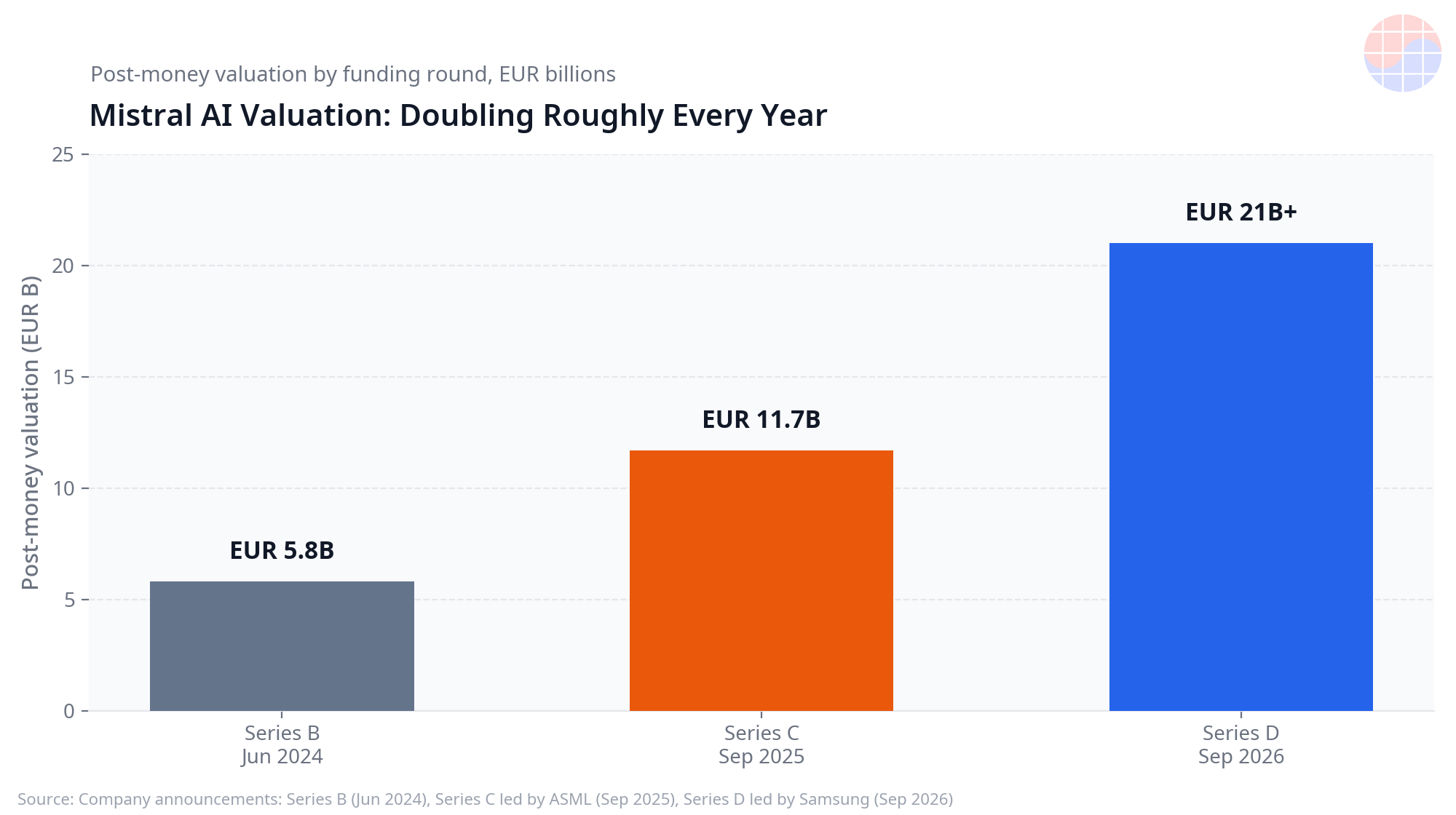
The valuation path shows how quickly the partner has grown.
| Round | Timing | Details | Valuation |
|---|---|---|---|
| Series B | June 2024 | Early large raise | EUR 5.8 billion |
| Series C | September 2025 | Led by ASML, EUR 1.7 billion raised | EUR 11.7 billion |
| Series D | September 2026 | Led by Samsung, EUR 3 billion raised | More than EUR 21 billion |
The path above is based on company announcements and reporting (company announcements and reporting, Sep 8, 2026). A rise from EUR 5.8 billion in June 2024 to more than EUR 21 billion in September 2026 does not by itself prove fab results. It does, however, mean Samsung entered not only as a customer but also as a lead investor and industrial partner, which gives the partnership more weight than a one-off pilot (company announcement, Sep 8, 2026).
The figures presented for Mistral AI itself need to be read as self-reported. The company has been presented as having more than 125 enterprise customers across 20 countries, with Airbus, ASML and HSBC named among them, ARR of more than USD 400 million in February 2026, and a target of USD 1 billion in ARR by the end of 2026 (company remarks, February 2026 and 2026 target). Those ARR and customer figures are self-reported by the company, not audited figures (company self-reported figures, Sep 8, 2026 announcement materials).
Deep Dive: What the Partnership Actually Does Inside the DS Division
The partnership integrates Mistral AI services and solutions, including the flagship LLM Mistral Large, across Samsung's semiconductor business and co-develops custom on-premise AI models tailored to DS division data (company announcement, Sep 8, 2026). Two words matter here: custom and on-premise. This is not described as taking a general-purpose model as-is. It is described as developing models for DS data (company announcement, Sep 8, 2026).
The stated application areas are data analysis, defect prediction and defect detection, and equipment and process optimization (company announcement, Sep 8, 2026). The goals are to shorten the design cycle, improve manufacturing precision and quality, and stabilize yield for advanced memory and logic chips (company announcement, Sep 8, 2026).
In operational terms, these areas connect. If defect data can be integrated quickly, correlations with process conditions become easier to find. If equipment state and process variables are viewed together, optimization has a starting point. In design, the speed of searching and organizing large internal data sets affects the design cycle. That is an interpretation of the application areas and goals in the announcement, not a disclosure of specific improvement figures, because no such figures were disclosed (company announcement, Sep 8, 2026).
Deep Dive: Why On-Premise Is the Real Story
In the on-premise structure, sensitive technology and operations data are processed only inside the boundary of Samsung's semiconductor infrastructure, with no transfer to an external cloud, and blocking technology leakage risk is presented as the core of the design (company announcement, Sep 8, 2026).
Yield and process data are crown-jewel assets for a simple reason. The asset is not just the final yield number. It is the full record of the conditions under which yield broke down and the actions that restored it. If that data flows into external model training or external storage, years of trial and error accumulated by the fab flow out with it. For AI inside a fab, the first requirement is therefore not performance. It is boundary design.
The choice has a cost. On-premise trades security for an operating burden that Samsung carries directly, including model updates and GPU infrastructure operations, and that burden is part of the honest limits of this partnership (analysis based on the company announcement, Sep 8, 2026). Work that an external service provider would normally handle has to be handled by the internal organization. Stronger security means more operating responsibility moves inside.
Deep Dive: Yield Economics — What 1 Percentage Point Is Worth
Yield is a percentage, but in a fab it converts directly into money. With the same wafer input, a different good-die ratio immediately changes the number of chips that can be sold.
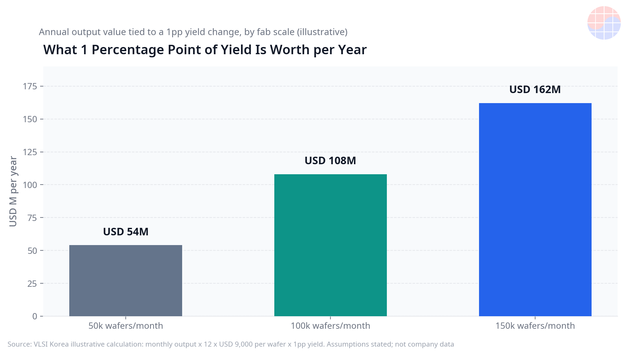
Here is a VLSI Korea illustrative calculation, with assumptions stated explicitly. Assume 100,000 wafers per month, USD 9,000 per wafer, and 12 months per year. On those assumptions, annual input value is 100,000 multiplied by 12 multiplied by USD 9,000, or USD 10.8 billion, and 1 percentage point of yield corresponds to 1 percent of that, or about USD 108 million per year (VLSI Korea illustrative calculation, assuming 100,000 wafers per month and USD 9,000 per wafer, as of Oct 21, 2026).
| Monthly volume | Annual input value | Annual value of 1 percentage point of yield |
|---|---|---|
| 50,000 wafers | USD 5.4 billion | USD 54 million |
| 100,000 wafers | USD 10.8 billion | USD 108 million |
| 150,000 wafers | USD 16.2 billion | USD 162 million |
The table applies the same VLSI Korea illustrative calculation and the same USD 9,000 per wafer assumption at every volume (VLSI Korea illustrative calculation, as of Oct 21, 2026). In a real fab, the result changes with product mix, node and wafer price, so this calculation shows direction and scale. It is not an estimate for any specific fab.
Even with that caveat, the point is clear. An improvement of even 0.1 percentage point can accumulate to tens of millions of dollars per year in a large fab, and yield instability destroys value at the same rate. The sensitivity is larger for HBM, where the process is long and stacking adds steps, and for foundry, where winning and keeping customers depends on yield stability. That is why the partnership explicitly names yield stabilization as a goal (company announcement, Sep 8, 2026).
Chase's Take
A precedent makes the picture sharper. ASML has also been collaborating with Mistral AI on R&D, engineering and operations AI and led the Series C, and Samsung, a chip maker, has now joined by leading the Series D (company announcements, September 2025 Series C and Sep 8, 2026). Both an equipment maker and a chip maker are pulling the same AI partner inside fab operations. That, more than the headline valuation, is the essence of this trend.
The honest limits matter just as much. First, no yield improvement has been publicly verified with any figure yet, and the announcement is a declaration of direction, not a result (company announcement, Sep 8, 2026). Second, an LLM has a different role from dedicated vision models such as defect image classification. The natural place for an LLM is the data integration, reporting and agent-style analysis layer. Third, Samsung directly carries the on-premise operating burden. Fourth, Mistral AI's ARR and customer numbers are self-reported, not audited (company self-reported figures, Sep 8, 2026 announcement materials).
My judgment is this. The value of the partnership will not be decided by launch-day expectations. It will be decided by whether Samsung built a structure that raises AI usage without sending fab data outside. The structure itself points in the right direction. In a fab, data is both raw material and finished product, and without a design that protects that boundary, no model can be used for long. The remaining question is execution: in which process, by which metric, and from when an improvement can be confirmed.
Implications
- The competitive axis for fab operations AI shifts from whether a model is adopted to how the data boundary is designed, and the stated reason for the on-premise structure is itself evidence of that shift (company announcement, Sep 8, 2026).
- For the Samsung DS division, the ability to treat fab data as an asset becomes more important, because co-developing custom models is about building internal data capability, not simply buying an external product (company announcement, Sep 8, 2026).
- In HBM and foundry, yield stabilization is directly linked to customer trust, so even a small yield improvement carries large business value, as the VLSI Korea illustrative calculation shows (VLSI Korea illustrative calculation, as of Oct 21, 2026).
- The sequence of an equipment maker, ASML, followed by a chip maker working with the same partner suggests fab operations AI may become a common layer connecting equipment and manufacturing (company announcements, September 2025 and Sep 8, 2026).
- Verification remains open. Until disclosed yield figures and audited business figures appear, the soundness of the structure and the results of execution should be evaluated separately (company announcement, Sep 8, 2026).
This article is analysis based on company announcements and reporting, is not investment advice, and unverified items such as yield effects should be read only within the limits stated in the text.
FAQ
Q1. What did Samsung Electronics and Mistral AI announce, and when? A1. On Sep 8, 2026, on the occasion of the Korea-France summit at the Elysee Palace in Paris, the two companies announced a strategic partnership in which Samsung led Mistral AI's Series D and agreed to integrate Mistral AI services, including Mistral Large, across its semiconductor operations (Samsung announcement, Sep 8, 2026).
Q2. Why does on-premise deployment matter? A2. Yield and process data are crown-jewel assets that cannot leave the fab, so the core design is to process sensitive technology and operations data only inside Samsung's semiconductor infrastructure boundary, with no transfer to an external cloud (company announcement, Sep 8, 2026).
Q3. How much is 1 percentage point of yield worth? A3. In a VLSI Korea illustrative calculation assuming 100,000 wafers per month and USD 9,000 per wafer, 1 percentage point corresponds to about USD 108 million per year, and the result changes with the assumptions and is not a verified performance figure.
Q4. Has a yield improvement already been verified? A4. No. No yield improvement has been publicly verified with any figure yet, and the announcement as of Sep 8, 2026 is a statement of direction, not confirmed performance (company announcement, Sep 8, 2026).
📩 Subscribe to VLSI Korea
Get our daily semiconductor deep-dives delivered to your inbox first. Free to subscribe.