VLSI Korea
Applied Materials Opens Its $5 Billion EPIC Center: The New Economics of Process R&D
Applied Materials opened its $5B EPIC Center in Sunnyvale on Oct 12, 2026 — a bet on shortening process R&D learning cycles after losing CHIPS Act funding. TSMC, Intel, Samsung, Micron, and SK hynix are founding partners. No Korean equipment maker is on the roster.


The bottom line: why an equipment company is building a $5 billion R&D factory
Applied Materials, the world's largest semiconductor equipment maker, unveiled its EPIC (Equipment and Process Innovation and Commercialization) Center on October 12, 2026, on its Sunnyvale, California campus. At roughly $5 billion, it is the largest collaborative R&D facility for semiconductor process and equipment in the world.
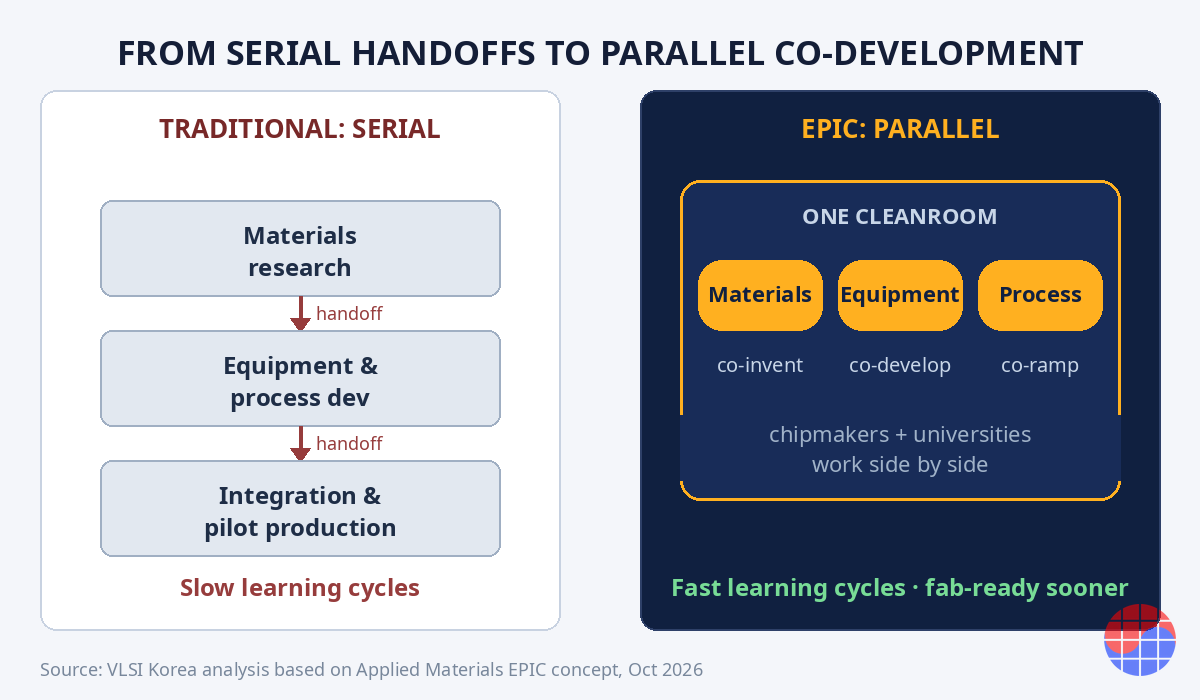
More important than the building is the business model. On the premise that at atomic-scale process nodes no single company can innovate alone, the center puts the people who invent materials, the people who build equipment, and the people who make chips in the same cleanroom and has them develop in parallel. TSMC, Intel, Samsung Electronics, Micron, and SK hynix are all on the roster as founding partners.
This is a signal that the cost structure of process innovation is changing. And for Korea's two memory makers, it represents a strategic asset: early access to next-generation process technology.
What happened: the facts (as of October 12, 2026)
- Announcement: Applied Materials official press release (GlobeNewswire, October 12, 2026), with an opening event on the Sunnyvale campus.
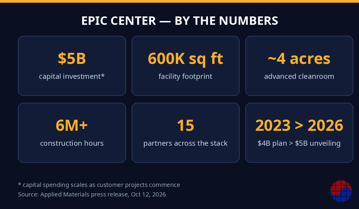
- Investment: Approximately $5 billion, to be deployed in phases as customer projects commence. This is up from the $4 billion announced when the project was first revealed in May 2023.
- Scale: A 600,000 sq ft (about 55,700 m²) building with roughly 4 acres (about 16,000 m²) of advanced cleanroom. Construction required more than 6 million hours of labor; the concrete used equals 34 Olympic-size swimming pools, and the steel equals two Eiffel Towers. Each of the 34 roof trusses spanning the cleanroom is about 300 feet (about 91 m) long.
- Core concept: Dismantling the conventional serial development model — in which fundamental materials research, equipment and process development, and process integration and pilot production happened in separate environments with a handoff at every stage. At EPIC, all three domains innovate in parallel under one roof.
- Founding partners (chipmakers): TSMC, Intel, Samsung Electronics, Micron, SK hynix
- Innovation partners: Broadcom, Advantest, SCREEN, KIOXIA, Besi
- Research partners: Arizona State University, Rensselaer Polytechnic Institute (RPI), Stanford University, UC Berkeley, UCLA Samueli School of Engineering
- Event: A summit of global chip industry R&D leaders, hosted by Prabu Raja, President of Applied Materials' Semiconductor Products Group.
Background: from the 2023 announcement to the 2026 opening
The EPIC Center is not new news. According to Reuters reporting on May 22, 2023, Applied Materials announced plans to invest up to $4 billion over seven years, hire 2,000 engineers, and conduct roughly $25 billion of research over the facility's first ten years. The cleanroom was then described as roughly the size of three American football fields.
There were setbacks along the way. According to Bloomberg, Applied Materials was rejected in its application for funding under the U.S. CHIPS and Science Act. It has decided to spend $5 billion without government subsidies. The contrast with 2023 is sharp: CEO Gary Dickerson said at the time that "scale and pace depend on government incentives." The 2026 message is unambiguous — this is an investment the company has to make whether or not the subsidies come.
Why $5 billion: the "cost disease" of process innovation
Prabu Raja's explanation cuts to the heart of it. At today's atomic-scale dimensions, many materials and material interfaces behave in entirely new ways, and making them work at industrial scale demands "coordinated development and integrated solutions."
To put it in the language of an engineer who has taped out chips: as scaling advances, signoff margins are tied directly to process variation. From my perspective as an STA engineer, half the battle of closing timing in PrimeTime comes down to how realistic the foundry's variation models are. And we now live in an era when the variation models themselves are being built for new materials and new structures — backside power delivery, hybrid bonding, and the like. Under the old serial model, where equipment, materials, and processes were developed separately and exchanged as files, the learning cycle is simply too slow.
In other words, EPIC's $5 billion is not a bet on a building; it is a bet on shortening the learning cycle. The figure Applied Materials put forward in the 2023 announcement — cutting the time from a university research idea to a production tool in the fab to nearly one-third — remains the justification for the 2026 opening.
Anatomy of the business model: the economics of a platform
The returns Applied Materials expects are two-sided.
What chipmakers get: early access to next-generation materials and equipment, shorter learning cycles, and a faster path to production. TSMC Chairman and CEO C.C. Wei said that "beyond 2nm, collaboration with Applied gives us early access to disruptive equipment technologies that will define the future." Intel CEO Lip-Bu Tan referenced the roadmap of "more than one trillion transistors per package by 2030," stressing close collaboration with equipment partners.
What Applied Materials gets: more important. In the words of the official press release, the company gains visibility into "emerging technology challenges" across multiple generations, uses that visibility to decide where to concentrate R&D investment, and gets its systems "designed in" to customer fabs. The company that sees customers' roadmaps first sets the equipment specifications. That is the strongest moat in the equipment industry.
In numbers: the 2023 plan — roughly $25 billion of research over the first ten years — represents five times the leverage on the $5 billion investment. That multiple is possible because customers and partners share the research cost. This is why the company pushed ahead even after being shut out of the CHIPS Act: it is a platform economics structure that works without subsidies.
The imec contrast: neutral consortium vs vendor-led
At this point, it is impossible not to think of imec in Leuven, Belgium. With more than 600 partners, imec is a neutral R&D consortium — the very emblem of open innovation built on shared pilot lines. EPIC is the model standing on the opposite side: vendor-led collaboration driven by the world's No. 1 equipment maker.
The differences come down to three things.
- Who captures roadmap visibility: At imec, research outcomes are broadly shared among partners by design. At EPIC, Applied Materials sits in the position of seeing every generation's technology challenges first.
- Who decides equipment specifications: Chipmakers in EPIC can influence tool design before it is finalized. Companies outside the tent — customers of Tokyo Electron or Lam Research, for instance — must adapt to finished specifications.
- Competitive dynamics: TEL, Lam, and ASML are not going to sit still. Vendor-led, large-scale collaborative R&D is likely to become the industry's standard playbook, which will only entrench the oligopoly structure of the equipment industry.
The neutral model is one everyone uses but no one monopolizes. The vendor-led model deepens the moat of whoever leads it. Applied Materials chose the latter.
Implications for Korea: early access for the two memory makers
From Korea's perspective, one fact matters most. Samsung Electronics and SK hynix are founding partners. Song Ja-hyuk, CTO of Samsung's DS Division, spoke of an end-to-end perspective spanning leading-edge logic, memory, and advanced packaging. Nohjung Kwak, CEO of SK hynix, directly cited "major inflections" across HBM, DRAM, and NAND. The next round of memory process competition will likely be decided in memory architectures beyond HBM4 — and Korea's two companies are standing at the starting line of that learning cycle.
On the other hand, no Korean equipment maker appears on the founding roster. The innovation partners include Japan (Advantest, SCREEN) and the Netherlands (Besi). For Korea's equipment ecosystem — where front-end equipment localization remains an unfinished task — this is a painful gap. While next-generation process learning happens in Sunnyvale, the absence of a Korean equipment company at that table is not a matter of pride; it is a matter of having a voice in how equipment specifications get decided over the next five years.
One more point: Micron is also a founding partner. With all three memory makers under one roof, memory process competition has now fully moved to the speed dimension — who learns faster. Whether EPIC's "tight, secure learning cycles" are actually secure cannot be verified from the outside — but the very fact that rival companies' engineers will work in the same facility says something about the level of trust in this industry.
Risks and counterpoints
For balance, three counterarguments.
- The $5 billion payback risk: This is money being spent from Applied Materials' own pocket after the CHIPS Act rejection. If customer projects do not materialize as expected, Applied Materials shareholders bear the cost. The phrasing that the investment of "approximately $5 billion" will "scale" as customer projects commence can also be read the other way: it is a demand-linked investment.
- The IP isolation question: TSMC, Intel, and Samsung will be doing research in the same facility. Applied Materials touts "tight, secure learning cycles," but there is no way to verify that from the outside. It is entirely possible that participating companies keep their core IP in their own fabs.
- The historical lesson of consortia: The history of large semiconductor consortia — SEMATECH, founded in 1987 — shows both the successes and the limits of the model. Collaborative R&D is no panacea, and Applied Materials knows that as well as anyone.
Figures and quotes in this article are based on the Applied Materials official press release (October 12, 2026), Reuters (May 22, 2023), and Bloomberg reporting; undisclosed items such as per-partner cost-sharing are not included.
FAQ
What exactly is the EPIC Center?
The EPIC (Equipment and Process Innovation and Commercialization) Center is an approximately $5 billion collaborative R&D facility for semiconductor process and equipment built by Applied Materials in Sunnyvale, California. Its core concept is performing materials research, equipment and process development, and process integration and pilot production in parallel under one roof, with 15 partners including TSMC, Intel, Samsung Electronics, Micron, and SK hynix. (As of October 12, 2026)
Why invest $5 billion after being rejected for CHIPS Act support?
According to Bloomberg, Applied Materials was rejected in its CHIPS Act funding application. It proceeded anyway because the structure works without subsidies: with customers and partners sharing research costs, roughly $25 billion of research over the first ten years (per the 2023 plan) rides on top of the $5 billion investment. In exchange, Applied Materials gains visibility into customer technology roadmaps across multiple generations.
How is it different from imec in Belgium?
imec is a neutral R&D consortium, while EPIC is a vendor-led model driven by the world's No. 1 equipment maker. Where imec shares research outcomes broadly among partners, EPIC puts Applied Materials in the position of seeing technology challenges first and reflecting them in equipment specifications. The defining difference is a structure that favors the leader.
What does it mean for the Korean semiconductor industry?
With Samsung Electronics and SK hynix joining as founding partners, they gain early access to next-generation logic, memory, and advanced packaging technologies — standing at the starting line of the learning cycle for the next major inflections in HBM, DRAM, and NAND. However, the absence of any Korean equipment maker on the founding roster remains a challenge for the front-end equipment ecosystem.
Disclosure
This article is the author's independent analysis based on public press releases (Applied Materials, October 12, 2026; Reuters, May 22, 2023) and published media reports. Mention of any specific company is not an investment recommendation; the author has no financial interest in the companies mentioned. This is not investment advice.