VLSI Korea
Copper's Last Stand: Why 448G PAM6 and PTFE Are Delaying the CPO Crossover
In the 576-GPU rack era, the real battle is signal integrity. 448G PAM6, PTFE substrates, and active copper buy copper one to two more generations, pushing the CPO economic crossover into the 2028–2030 window.


Copper's Last Stand: Why 448G PAM6 and PTFE Are Delaying the CPO Crossover
The 30-Second Version
- The AI infrastructure debate is always about GPUs and HBM. But when 576 GPUs move into a single rack — NVIDIA's Vera Rubin Ultra NVL576, scheduled for 2027 — the real battleground becomes signal integrity, not compute.
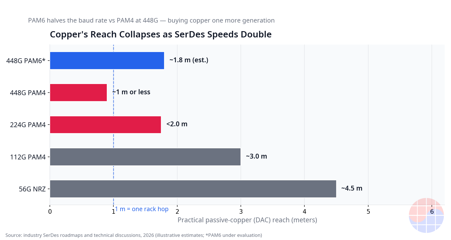
- Physics is unforgiving. At 224G SerDes, a passive copper cable reaches well under 2 meters; at 448G it drops to roughly 1 meter (industry discussion as of 2026). The skin effect and the Nyquist frequency set the limit — that barely spans a rack.
- So the industry chose extension over surrender. Three weapons keep 448G copper alive — PAM6 modulation, low-loss PTFE laminates, and ultra-dense cable assemblies — all on display at the NVIDIA MGX ecosystem showcase at the OCP Global Summit in October 2026.
- Optics is accelerating too: MACOM's 448G/lane PAM4 drivers (over 120 GHz RF bandwidth, March 2026), the Keysight–NTT–Lumentum 448G demo (OFC 2025), and TSMC COUPE's 2026 target for CoWoS-based CPO integration.
- But this article's core thesis is one sentence: the gate to CPO volume production is not photonics physics — it is test throughput. Wafer-level PIC testing, double-sided probing, and fiber attach set the slope of the production ramp.
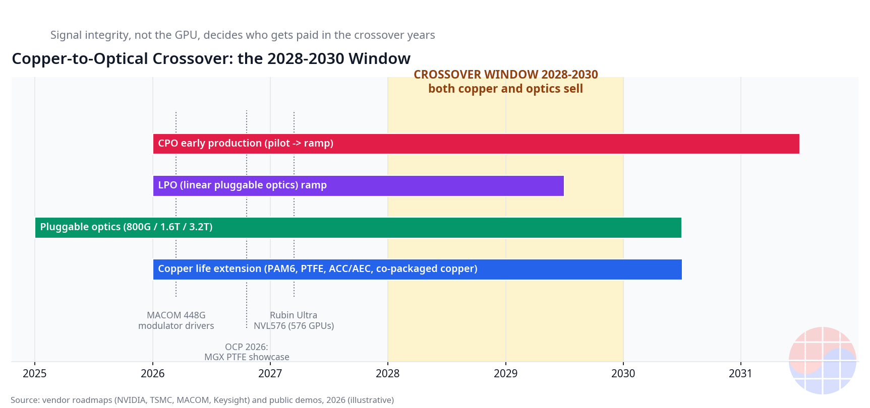
- Bottom line: the copper-to-optics economic crossover is sliding into a crossover window in 2028–2030. The winners of that window won't be GPU companies. They will be the companies that keep the signal alive — SerDes, low-loss materials, active copper, and optical test equipment.
Background: The Rack Is the Computer
In 2020, the average data center rack drew 8.2 kW. In 2025, NVIDIA's GB200 NVL72 (72 GPUs) hit 132 kW per rack. The roadmap keeps going: after Rubin NVL144 (2026) comes Rubin Ultra NVL576 (2027) — 576 GPUs in one rack, four pods, 18 blades per pod, 8 GPUs per blade, with industry analysis in 2026 putting peak power in the megawatt class.
Inference architecture is changing too: splitting prefill (compute-intensive, reading the prompt) from decode (memory-bandwidth-intensive, generating tokens one by one) onto different GPU groups — disaggregated inference — became the standard design language of 2026, with the KV cache moving between node types over RDMA so fabric traffic explodes.
The SerDes roadmap collides with both: 56G NRZ → 112G PAM4 → 224G PAM4 (IEEE 802.3dj in progress) → 448G next. The rule of thumb: double the speed, and copper's reach roughly halves. Skin-effect losses steepen as frequency rises, and the Nyquist frequency — tied to the modulation scheme — sets the ceiling.
So AI infrastructure now sits where three waves crash at once: (1) exploding GPU counts per rack, (2) exploding fabric bandwidth from prefill/decode separation, and (3) collapsing copper reach as SerDes speeds double. The answer to "what's the bottleneck after the GPU?" is signal integrity.
The fabric has a dual structure. Scale-up — GPUs bound directly together (NVLink) — is copper territory today. Scale-out — racks stitched together (Ethernet, InfiniBand) — is already optics territory. Copper survived the 224G era because scale-up distances stayed inside the rack. But with 576-GPU racks and multi-rack NVLink domains arriving, scale-up distance grows too. The economics of this article begin exactly at the boundary where copper's territory gets invaded by optics' territory.
Deep Dive
1. How Copper Fights Back: Three Weapons
For copper to survive 448G, it has to win the war against channel loss — the industry's answer is three weapons.
First, modulation: PAM6 under serious consideration. Push 448G over PAM4 and you need 224GBaud, with a Nyquist frequency of 112 GHz. Send the same 448G over PAM6 and the baud rate drops to roughly 149GBaud, Nyquist to about 74.5 GHz. Since channel loss scales with frequency, lowering the baud rate is a direct loss reduction for the copper channel. The price: six levels instead of four shrink the signal-to-noise (SNR) margin and raise the forward error correction (FEC) and DSP burden — and stronger FEC adds latency, which in a scale-up fabric is GPU idle time. Keysight stated in an April 2025 release that it was exploring diverse modulation formats for early 448Gbps R&D. In other words, 448G copper's modulation scheme is still undecided — and undecided means a one-to-two-generation design window before the standard hardens.
Second, materials: PTFE. At 224G/448G lanes, the PCB trace itself — not the connector or the cable — accounts for a large share of channel loss. With a conventional FR-4 dielectric loss factor (Df), 100 GHz-class signals struggle to travel even a few tens of centimeters. Dielectric constant (Dk) sets signal speed and impedance; the loss factor (Df) sets the energy lost as heat. The flagship material that gets both low at once is the fluoropolymer laminate PTFE. Megtron-class low-loss FR-4 variants are the alternative, but beyond 224G toward 448G, the consensus is that only PTFE-class materials can close the channel budget. That an "NVLink PTFE Board" was one axis of the October 2026 OCP Global Summit's NVIDIA MGX ecosystem showcase — with thirteen companies across PCB, advanced materials, connectors, and cable assemblies — is symbolic. Substrate selection is now part of rack design competitiveness.
Third, connectors and cables: bring copper to the chip. The other axis of that same showcase was the "Ultra Dense Interconnect Cable Cartridge." The concept is simple and powerful. Ultra-dense near-chip connectors minimize PCB trace length; twinax-based high-density cables bring copper directly up to the chip. The industry calls it co-packaged copper. Instead of fighting trace loss, it routes around it. Molex's Impress co-packaged copper solution supports 224Gbps PAM4 today and is being developed toward 336G and 448G. Then active copper (ACC/AEC) extends reach further: retimer and redriver DSPs at both cable ends buy a few more meters in exchange for more power — paying watts to buy copper's lifetime. The math underneath assumes it can still undercut an optical module's DSP power.
Alchip and Synopsys jointly announced in September 2026 that they solved die-edge escape routing and package breakout problems for 224Gbps SerDes scale-up interconnects through system-level optimization, with the methodology extendable toward 448G SerDes. Copper still holds cards.
2. The Optical Counterattack: 448G Photonics Is Out of the Lab
Meanwhile, optics isn't waiting.
Keysight, NTT Innovative Devices, and Lumentum (April 2025, OFC 2025) demonstrated 448Gbps data transmission with 224GBaud PAM4 optical technology. Two Keysight M8199B arbitrary waveform generators and NTT's frequency-domain interleaver produced the electrical signal, transmitted through Lumentum's InP EML — targeting power-efficient 3.2T optical interfaces.
MACOM (March 17, 2026, OFC 2026) released two 448G/lane PAM4 modulator drivers — the MAOM-025408 (Mach-Zehnder driver) and MAOM-022404 (EML driver) — both delivering over 120 GHz of RF bandwidth and supporting silicon photonics, EML, and TFLN modulators alike. These are the parts meant to pull 1.6T and 3.2T optical transceivers into the market — matching copper's next-generation per-lane speed, so the two camps fight over the same SerDes physics.
The middle ground is opening too. LPO (linear pluggable optics) strips out the DSP and uses linear direct drive to cut power — a pluggable module that keeps the established ecosystem (field-replaceable, mature supply chain) and only trims watts. If CPO is the revolution — putting the optical engine inside the package — LPO is the refinement: keep the pluggable form, lower the power. Refinements make money while revolutions run late.
And the big CPO picture. TSMC's COUPE (Compact Universal Photonic Engine) stacks the electrical die (EIC) directly on the photonic die (PIC) with SoIC-X chip stacking. The roadmap: small-form-factor pluggable qualification in 2025, CoWoS-based CPO integration in 2026 — with TSMC citing 5–10x power efficiency improvement and 10–20x lower latency. NVIDIA (GTC 2025) answered with CPO networking switches — Quantum-X and Spectrum-X — using micro-ring modulators for density and claiming 3.5x power efficiency and 10x resilience over conventional networks. Samsung joined the field at OFC 2026, mentioning a 2027 optical engine and a 2029 turnkey CPO service.
Even the pluggable camp has played its last card. At OCP 2026 (October 2026), NVIDIA and Cisco announced USFP (Ultra-Dense Small Form Factor Pluggable) — a new form factor targeting 400G/lane, 16 lanes per module (6.4T), and 32 lanes (12.8T) later. With front-panel density at its limit, the module itself got redesigned — yet USFP still insists on being 'pluggable.' Even NVIDIA is keeping a middle path open: "go optical now, take CPO slowly."
3. The Real Gate Is Testing
TSMC's packaging leadership has publicly named the three challenges for CPO volume production: wafer-level testing, fiber array unit integration, and high-speed optical packaging assembly — and the first is the one that strangles the ramp.
The reason is structural. In a COUPE-style stack, the hybrid bonding that joins the electrical and photonic dies cannot be reworked. Discover a defect only after the engine is bonded onto an expensive switch or GPU package, and yields disintegrate — so both dies must be optically probed before bonding, at the engine level. Engine yield is EIC yield × PIC yield × bonding yield × coupling yield — the curse of multiplication.
Test equipment makers are already moving. FormFactor and Advantest formed a strategic partnership for wafer-level test cells for silicon photonics and CPO — 9-axis nano-precision automated optical alignment, integrating Advantest's V93000 ATE with FormFactor's Velox probe stations. FormFactor projected 2026 CPO-related revenue to "significantly exceed" $20 million (Q2 2026 earnings call). Teradyne unveiled the Photon 100 at OFC 2026: double-sided probing for COUPE-style stacks, where electrical contacts sit on one face and optical ports on the other.
The summary: the slope of the CPO production ramp is set by how fast test equipment gets installed. Test throughput is CPO shipments.
4. The Economics of the Crossover: The Inflection Arrives as Curves, Not Technology
The winner isn't the "better technology" — it's whichever cost-per-bit and power-per-bit curve crosses first.
Pushing the copper curve down: PAM6 (lower baud rate, less channel loss), PTFE (less dielectric loss), ACC/AEC (pay power, extend reach). Pushing the optics curve down: LPO (drop the DSP, cut power), CPO (package integration for power and density), USFP (pluggable density innovation).
The key question: what happens if copper survives one or two more generations at 448G? The optical economic crossover gets pushed back. The moment CPO becomes "cheaper and more power-efficient than copper" slides into a crossover window in 2028–2030. This is a "both sell" window: copper's last harvest season and optical test equipment's golden age. LPO is the wild card here. Because it keeps the pluggable ecosystem while cutting power, it could pull the crossover forward — ahead of CPO.
5. The Other Side: Why CPO Could Arrive Sooner
First, power. In the era of hundreds-of-kilowatts — soon megawatt-class — racks, the interconnect's share of power can't be ignored. TSMC's 5–10x power efficiency claim for CPO is photonics' strongest weapon.
Second, density. Put 576 GPUs in a rack and front-panel area hits a physical limit. If even pluggable innovations like USFP fall short, packaging the optical engine inside the package — CPO — becomes the only answer. NVIDIA's OCP 2026 preview of Rubin Ultra as a "CPO-based NVLink fabric connecting 576 GPUs" is the peak of this argument.
The rebuttal. Roadmaps are not production. Between "CPO works" and "CPO ships at yield" lies the canyon of testing. And NVIDIA itself played the USFP pluggable card simultaneously — a sign that even they know how long the transition window will be. The early-CPO case isn't wrong; its clock just needs recalibrating to test throughput.
Chase's Take
Any engineer who has signed off timing in PrimeTime will nod at this sentence: "You can't tape out on an uncovered timing path."
CPO is exactly the same. It's not the physics of the photonic die that matters — it's the "engine yield proven by testing" that separates production from press releases. CPO's signoff is dual: an optical yield signoff stacked on top of the electrical signal-integrity signoff. An optical I/O without test coverage is like a netlist without timing closure. You can't ship it.
Through the MBA lens, this is a textbook case of crossover economics. The winner isn't the "most advanced technology" — it's whoever captures the transition window's cash flow. Copper's one-to-two-generation extension is the last supercycle for SerDes and DSP, PTFE laminates, and active cable makers. CPO test equipment is the picks-and-shovels of the optical transition. The window's economic rent doesn't flow to GPU companies — it flows to the companies that keep the signal alive. The thing to watch isn't the next page of the GPU roadmap; it's the breakeven point of signal integrity.
Implications: For Investors and Operators
For investors.
- Copper-extension winners. SerDes IP and DSP, retimers, active cable, low-loss materials (PTFE laminates). The catalyst: the direction of 448G PAM6 standardization — if PAM6 hardens, copper's life extends one more generation.
- Optical test equipment. The leading indicator and direct beneficiary of the CPO ramp: test-cell utilization and equipment orders move before CPO volumes themselves.
- CPO itself. Aggressive bets before 2028 risk capital getting stuck in the crossover window. LPO is the middle-ground wildcard, worth tracking separately.
For architects and operators. At 448G lanes, design the 1-meter reach assumption in from the start of the architecture. PCB stackup and material selection is no longer a downstream decision — it's part of rack competitiveness, and the precondition for a CPO roadmap isn't securing optical engines but securing the test supply chain.
Through the Korea lens. 2026 is Korea's AI infrastructure founding year: the National AI Computing Center (Samsung SDS consortium, May 2026 — KRW 2.5 trillion, 15,000 AI accelerators by 2028), Samsung's Chuncheon modular AIDC (July 2026, Blackwell-ready, October 2027 target), SK–AWS Ulsan (103 MW, ~60,000 GPUs, 2029), and Naver Gak Sejong (up to 270 MW). The AI Data Center Act (May 2026) accelerates non-metro builds.
Korea is mostly in the position of importing and building racks for now — but that is exactly where the opportunity sits. The high-frequency demands of Blackwell- and Rubin-class racks — low-loss PCB materials, high-density cable assemblies, signal-integrity validation — are the crossover window's direct beneficiaries. Copper's one-to-two-generation extension buys Korea's interconnect supply chain time to build cash flow before the optical transition.
FAQ
Q1: Why does PAM6 help 448G copper? Pushing 448G over PAM4 requires 224GBaud; PAM6 needs only about 149GBaud. A lower baud rate means a lower Nyquist frequency, which cuts frequency-dependent channel loss. The cost: six signal levels shrink the SNR margin and raise the FEC and DSP burden. As of 2026, the 448G copper modulation scheme remains under industry discussion.
Q2: Why did PTFE substrates suddenly become important? At 224G/448G lanes, the PCB trace itself — not the connector or cable — dominates channel loss. PTFE is a fluoropolymer-based low-loss, high-frequency laminate; its low dielectric constant (Dk) and low loss factor (Df) sharply cut dielectric loss at 100 GHz-class frequencies. The "NVLink PTFE Board" in the NVIDIA MGX ecosystem showcase at the October 2026 OCP Global Summit shows substrate selection has become part of AI rack competitiveness.
Q3: What's the difference between LPO and CPO? LPO (linear pluggable optics) is a pluggable optical module that drops the DSP and uses linear direct drive to cut power — a refinement that keeps the established pluggable ecosystem. CPO (co-packaged optics) puts the optical engine directly inside the switch or GPU package: a bigger leap in power and density, but with heavy manufacturing challenges in wafer-level testing and fiber attach.
Q4: When will CPO reach serious volume production? TSMC's COUPE targets CoWoS-based CPO integration in 2026, and NVIDIA and Samsung have published CPO roadmaps. But hybrid bonding can't be reworked, so wafer-level testing, double-sided probing, and fiber-attach throughput set the ramp. Given how test equipment (FormFactor, Advantest, Teradyne) is deploying, the reasonable base case for serious volume is after 2028.
Reach, power, and timing figures here are estimates based on public disclosures and industry technical discussion as of October 2026; actual product specifications and production schedules vary by vendor.
Sources
- MACOM, "Two New 448G per Lane Drivers for 3.2T Data Center Connectivity" (March 17, 2026, official press release)
- Keysight, NTT Innovative Devices, Lumentum, "448 Gbps Data Transmission" joint demo (OFC 2025, April 2, 2025, official press release)
- Alchip and Synopsys, "Address Scale Up and Out Bandwidth Constraints" (September 23, 2026, joint press release)
- FormFactor and Advantest strategic partnership on silicon photonics wafer-level test cells (joint announcement)
- NVIDIA OCP Global Summit 2026 presentations: MGX 1.2 contributions, Vera Rubin Ultra preview, USFP (NVIDIA and Cisco)
- Gangwon Ilbo, "Samsung to Build AI Data Center in Chuncheon" (July 6, 2026)
- Asia Business Daily, "Samsung SDS Consortium Confirmed for National AI Computing Center Project" (May 11, 2026)