VLSI Korea
Rapidus: Japan Plans Another 400 Billion Yen for 2nm, and a Medical AI Use Case Arrives
Japan plans 400 billion yen more in equity for Rapidus over FY2027-2029, taking state investment to 650 billion yen to support 2 trillion yen in private loans. A 2nm medical AI project adopted the same week gives the fab its first named use case, but validation starts only in FY2029.


Key takeaways
1. On October 19, 2026, the Ministry of Economy, Trade and Industry presented a plan at a subcommittee of the Fiscal System Council to invest an additional 400 billion yen in Rapidus over the three years from fiscal 2027 to fiscal 2029. Combined with the 250 billion yen already decided, cumulative government equity would reach 650 billion yen. The amount is not final: each fiscal year's request still needs approval before funds are disbursed.
2. The point of this money is equity, not subsidy. To borrow 2 trillion yen from private lenders, Rapidus has to hold its equity ratio, and the government is putting in capital to support that ratio.
3. The next day, October 20, a research project to build a medical imaging system around an inference-specialized 2nm-generation chip was adopted under a NEDO program. Its targets are 5 times the processing speed and 10 times the energy efficiency of current GPUs. In effect, Japan-made 2nm has gained its first concrete use case.
4. The schedules do not line up. Rapidus targets the start of mass production in the second half of fiscal 2027, while real-device validation of this medical AI chip starts only in fiscal 2029 or later. Filling the funding gap and filling the fab are different problems.
The money: 400 billion yen is capital, not a subsidy
Broken down by year, the plan presented by the ministry on October 19, 2026 is 150 billion yen in fiscal 2027, 150 billion yen in fiscal 2028, and 100 billion yen in fiscal 2029. The investment will be made as an industrial investment through the Information-technology Promotion Agency (IPA). The government already invested 100 billion yen in fiscal 2025 and 150 billion yen in fiscal 2026, so cumulative equity would reach 650 billion yen if the new plan is approved in full.
| Item | Amount | Status |
|---|---|---|
| Government equity (fiscal 2025-2026) | 250 billion yen | Decided, in execution |
| Additional equity, fiscal 2027 | 150 billion yen | Budget request |
| Additional equity, fiscal 2028 | 150 billion yen | Planned request |
| Additional equity, fiscal 2029 | 100 billion yen | Planned request |
| Cumulative government equity (if all approved) | 650 billion yen | Not yet final |
| NEDO R&D contracts approved, cumulative (fiscal 2022-2026) | About 2.354 trillion yen | Approved |
| Loans planned from private financial institutions | 2 trillion yen | Letters of intent received, execution under negotiation |
| Equity target from private companies | About 1 trillion yen in scale | Fundraising under way |
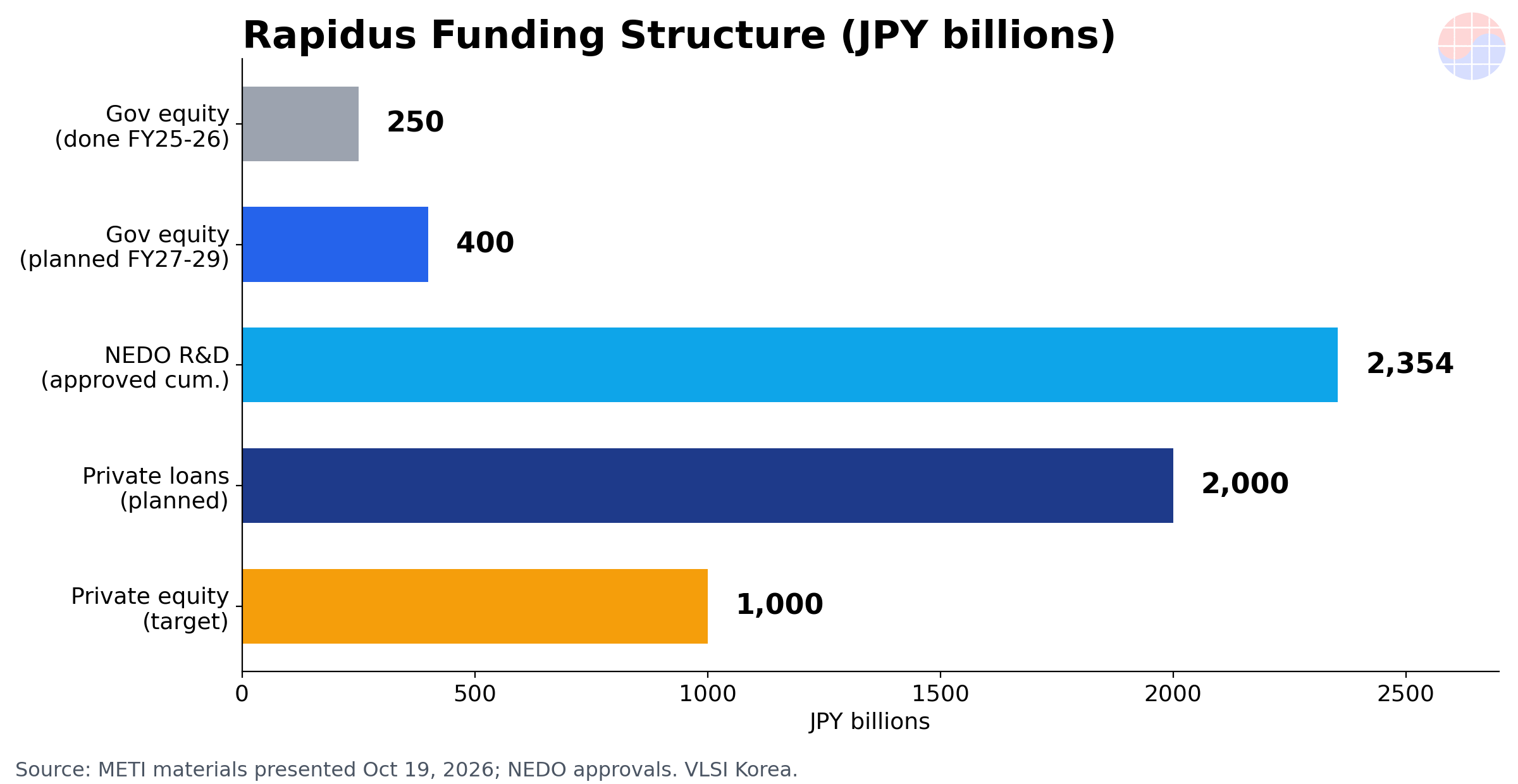
Why it has to be capital is the core of this case. The equity-ratio benchmarks cited in the ministry material are 50.4% on average for manufacturing, 61.0% for semiconductor-related manufacturers, and 65.5% on average for the three companies TSMC, Intel and Samsung Electronics. A leading-edge fab spends on equipment first and waits years for revenue to follow, so a company funded only by borrowing would see its ratio collapse and its next loan blocked. Private lenders issued a legally non-binding letter of intent for 2 trillion yen in loans in 2025, and talks to move toward execution are now under way. A government debt guarantee is also part of the plan. The immediate goal is to raise about 400 billion yen first in fiscal 2027.
The research money has been piling up separately. In April 2026, Rapidus received approval from NEDO for a fiscal 2026 support ceiling of about 631.5 billion yen: about 514.1 billion yen for 2nm integration and short-lead-time manufacturing technology, and about 117.4 billion yen for chiplet package design and manufacturing technology. Together, approved R&D contracts for fiscal 2022 through fiscal 2026 total about 2.354 trillion yen. The latest material also lists a budget request of about 300 billion yen for fiscal 2027 R&D contracts. In short, this is a two-layer structure: R&D is carried by contract funding, while the balance sheet for mass production is carried by equity and loans.
The use case: 2nm medical AI, with Hokkaido University Hospital as the first real-world test site
On October 20, 2026, five parties — the Leading-edge Semiconductor Technology Center (LSTC), Hokkaido University, Fujifilm, GE Healthcare Japan and imec — announced that a new project had been adopted under NEDO's program to strengthen the foundations of post-5G information and communications systems. The project is research and development of a high-speed, low-power medical imaging system using an inference-specialized 2nm-generation semiconductor.
| System | What it does | Goal |
|---|---|---|
| Real-time diagnostic imaging support | High-speed reconstruction AI for large-volume photon-counting CT data, plus organ segmentation AI | Improve diagnostic accuracy and speed at the same time |
| Real-time clinical support | Real-time overlay of ultrasound images with CT and MRI images | Remove positioning delay during procedures |
| Real-time surgical support | Real-time measurement of instruments, anatomy and bleeding in surgical microscope video | Support decisions during surgery |
Development proceeds in two stages. Models are first built and optimized on IBM's AI accelerator, the Spyre Accelerator, and the results are then ported to an inference-specialized 2nm-generation AI chip. The numeric targets are at least 5 times the image-processing speed and at least 10 times the energy efficiency of current GPUs. The technology will be validated for clinical usefulness at Hokkaido University Hospital. The project runs from September 2026 to September 2031 and was presented as a contract program worth 6.2 billion yen through the stage evaluation in March 2029, and 10.5 billion yen in total.
Two points need to be stated precisely. First, the manufacturer has not been officially confirmed. The chair of LSTC, which leads the project, also chairs Rapidus, and at the announcement it was explained that the intended use is for Rapidus to manufacture, on a foundry basis, a chip designed by IBM. Given that the design starts from an IBM-family chip, Rapidus is indeed the most likely candidate, but no contract has been announced. Second, the project itself is a partial answer to the oldest question around Rapidus: who will pay for chips and place orders? For the first time there is a named use case whose end user is a hospital, whose validation site is a university hospital, and whose performance targets are written in numbers.
The timing gap: mass production in 2027, validation of this chip in 2029 or later
Rapidus's business plan calls for 2nm mass production to start in the second half of fiscal 2027, advanced packaging mass production in fiscal 2028, positive operating cash flow in fiscal 2029, and positive free cash flow and a stock listing in fiscal 2031. Real-device validation of the medical AI project's 2nm chip, however, starts only in fiscal 2029 or later, because the period up to the stage evaluation in March 2029 is for building the models on the existing Spyre accelerator.
What this gap means is clear. This use case is not volume that will support utilization at the fab in its early production phase. Even if the line starts running in 2027, this chip will not flow through it right away. Customers and volume to fill the period from the start of mass production to validation in fiscal 2029 or later have to come from somewhere else. Viewed from the other side, securing now a use case that will still be alive after 2029 can be read as laying a demand pipeline in advance for after the fab is built. Either way, there is one yardstick: how many customers actually tape out and place production volume in 2027 and 2028 is the number to check before the size of the equity package.
📩 Following this story?
Get the follow-up analysis — earnings, reports and HBM supply — in your inbox daily at 10:30 KST. Subscribe free →
The cost arithmetic also needs a cold look. A medical-only chip ships in small volumes. Public estimates put the cost of a full 2nm mask set at a very high level, so a dedicated chip built in the tens of thousands of units per year can hardly recover its mask and design costs. For this structure to work, the same chip has to spread into server or industrial inference and grow in volume. The IBM-family origin of the design makes that expansion possible — and also means the arithmetic fails if the chip stays confined to a single medical use.
A Korean perspective: a different funding structure, and the opportunity sits in design and verification
Korean semiconductor support centers on tax credits and infrastructure, while Japan's approach here is for the government to inject capital directly and prop up the equity ratio. The comparison is not about which is better; it is that fabless companies and foundries are financed in fundamentally different ways. Adding government equity of 650 billion yen to R&D contracts of 2.354 trillion yen gives a sense of the weight of public money Japan is placing on a single company.
The practical opportunity lies elsewhere. An inference-specialized chip differs from a training chip in the character of its design verification. In edge inference, where latency and power are constrained at the same time — medical imaging is the example here — the architecture is narrowed for a specific purpose, and in return timing closure, low-power verification and reliability verification at a functional-safety level become heavier. From the standpoint of STA, power analysis and DFT, a larger 2nm design ecosystem in Japan means growing demand for design services, verification talent and IP alongside it. For Korean companies, that is the immediate meaning, more than a competitive threat. Once 2nm design actually starts running in Japan, money flows first to whoever sells design automation tools and verification know-how.
The choice of medical AI as the use case carries a message of its own. Japan has hospitals and large medical-device makers at home, and it is a market where medical imaging demand grows structurally as the population ages. By choosing, as its first use case, demand that is absorbed domestically regardless of export controls or geopolitical risk, the selection fits the country's industrial structure.
Risks: approval, the ratio, and the customer count
First, the 400 billion yen is at the request stage. The fiscal investment and loan request has to be approved each year, and it has already been pointed out in the review process that policy value and profitability should be checked regularly to decide each year whether to proceed with the industrial investment. Second, an equity ratio is not maintained by equity injections alone. Losses in early mass production erode capital, so holding the ratio depends on yield and the pace of revenue. Third, the 2 trillion yen in loans is moving from the letter-of-intent stage into execution talks; it is not confirmed borrowing. Fourth is the customer problem. Medical AI is a good use case, but its volume sits in fiscal 2029 or later. The credibility of the whole plan will rise only when the list of customers that will fill the fab before then can be confirmed in published numbers.
The conclusion is simple. Japan has moved past the stage of attaching money to 2nm and into the stage of attaching a funding structure and a first use case. The remaining question is neither money nor use case, but time. What fills the two years between mass production in 2027 and real-device validation in 2029 is the real test of this project.
Frequently asked questions
Q. How much is the Japanese government investing in Rapidus in total?
A. If the additional 400 billion yen planned for fiscal 2027-2029 is approved on top of the 250 billion yen already decided, the cumulative total reaches 650 billion yen. The additional portion assumes approval in each fiscal year, so it is not yet a confirmed amount. (Material presented by the Ministry of Economy, Trade and Industry on October 19, 2026)
Q. Why equity rather than a subsidy?
A. Because Rapidus needs to maintain its equity ratio to borrow 2 trillion yen from private financial institutions. The ministry cited 61.0% as the equity-ratio benchmark for semiconductor manufacturers and 65.5% as the average for TSMC, Intel and Samsung combined.
Q. What will the 2nm medical AI project build?
A. Three systems on an inference-specialized 2nm chip: CT reconstruction, overlay of ultrasound with CT and MRI, and image recognition during surgery. The targets are 5 times the speed and 10 times the energy efficiency of current GPUs, with validation at Hokkaido University Hospital. (Adoption announced on October 20, 2026)
Q. Is it confirmed that Rapidus will manufacture the medical AI chip?
A. No, it is not officially confirmed. The design starts from an IBM-family chip and the leadership of the project lead organization overlaps with Rapidus, so Rapidus is cited as the most likely candidate, but no manufacturing contract has been announced.
Q. What are the Rapidus production schedule and targets?
A. The business plan targets 2nm mass production in the second half of fiscal 2027, advanced packaging mass production in fiscal 2028, positive operating cash flow in fiscal 2029, and positive free cash flow and a stock listing in fiscal 2031.
Chase's Take — The two announcements that came out of Japan this week have to be read together. One builds the financial structure by injecting capital, and the other shows where 2nm will be used. Both are progress, but neither fills the fab in 2027. The next number I will check is not the approved equity amount; it is how many outside customer chips actually enter tape-out in 2027 and 2028. Until that number appears, Rapidus is a project with money and a use case, not yet a fab with volume.
📩 Missed today's analysis? Get tomorrow's in your inbox
Daily Silicon at 10:30 KST plus earnings and analyst-report breakdowns, first. Samsung Electronics, SK hynix, TSMC and HBM supply, read by practicing engineers. Join 300+ subscribers.
Subscribe free →
Free · No spam · Unsubscribe anytime