VLSI Korea
Space Data Center Semiconductors 1: How Radiation Kills Chips — TID, SEE and Rad-Hard Design Basics
Radiation kills orbital chips two ways: TID degrades them slowly over years, SEE flips or destroys them in nanoseconds. ODC Episode 1 explains both and the rad-hard design stack that fights them.


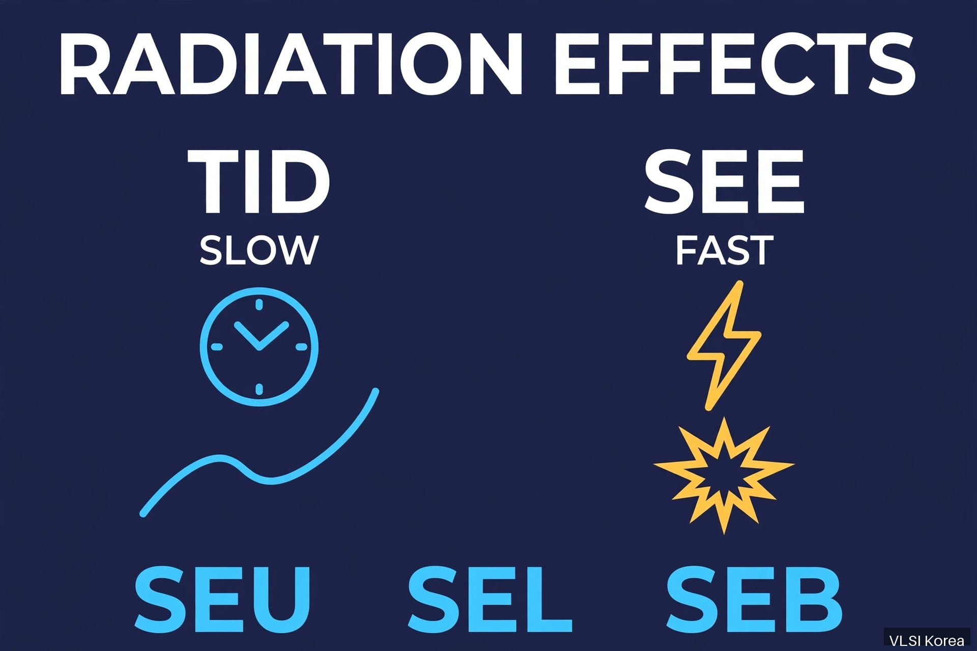
30-second summary. Radiation kills an orbital chip in two completely different ways. Total ionizing dose (TID) is a slow poison: trapped charge builds up in transistor oxides over months and years, shifting threshold voltages and raising leakage until the chip drifts out of specification. Single-event effects (SEE) are an instant hit: one heavy ion or proton deposits enough charge in picoseconds to flip a bit, hang a processor, latch up a power rail, or burn out a device — with no warning. As of 23 October 2026, every credible orbital data center (ODC) design is therefore built around the same stack: choose the orbit, budget the dose in rad(Si), harden the silicon with radiation-hardened-by-design (RHBD) techniques, correct what still gets through with ECC and redundancy, and qualify the whole thing by test. This is Episode 1 of the ODC semiconductor series, built on the Orbital Data Center Technical Report.
Put a terrestrial GPU on a satellite without changing anything else, and the silicon itself becomes the mission risk. Not the launch, not the link budget — the transistors. Earth protects its data centers with an atmosphere and a magnetosphere. Orbit removes both. What remains is a continuous flux of trapped protons and electrons, solar particle bursts, and galactic cosmic rays heavy enough to punch through a spacecraft wall and through a chip package as if neither existed.
This episode lays out the physics first, because every later episode in this series — COTS survival strategy, thermal design, power, optical links, memory, on-board AI, economics, players, and the Korean opportunity — depends on it. If you understand TID and SEE, you understand why space silicon looks the way it does.
Background: three radiation sources, one bad neighborhood
Space radiation comes from three sources, and each one attacks electronics differently (NASA and ESA radiation-effects literature, accessed 23 October 2026).
- Trapped radiation (Van Allen belts). Earth's magnetic field traps protons and electrons in two belts. This is the dominant, predictable dose source for Earth-orbiting systems, and it is worst where the inner belt dips closest to the planet: the South Atlantic Anomaly (SAA), a region over Brazil and the South Atlantic where the offset, tilted magnetic field lets trapped protons descend to low Earth orbit (LEO) altitudes. Most of the total dose a LEO satellite accumulates arrives during SAA passes, which recur on most orbits. Dosimeters flown on a recent commercial crewed LEO mission attributed roughly 44 percent of the crew's total absorbed dose to SAA crossings alone (reported 2026).
- Solar particle events. Flares and coronal mass ejections accelerate protons to high energies in bursts lasting hours to days. They are episodic, hard to schedule around, and they spike both dose rate and upset rate at exactly the moment the operator can do least about it.
- Galactic cosmic rays (GCR). Nuclei from outside the solar system, up to iron and beyond, at energies so high that practical shielding barely slows them. Their flux is low, but a single heavy ion carries the highest linear energy transfer (LET) — energy deposited per unit path length, measured in MeV·cm²/mg — and LET is what makes single-event effects destructive.
Altitude and inclination decide which source dominates. A 500 to 600 km equatorial orbit is comparatively benign. A polar or sun-synchronous orbit crosses the high-latitude horns of the belts and the SAA far more often. Higher LEO near 1,400 km sits inside the proton belt and can be harsher than geostationary orbit (GEO) for total dose. There is no single "space dose" — there is only a mission dose, computed orbit by orbit.
| Orbit (reference mission) | Typical TID behind shielding | Design implication |
|---|---|---|
| LEO, about 800 km, 3–5 years | About 3–5 krad(Si) | Carefully selected COTS can survive with system-level protection |
| LEO, about 1,400 km, 5 years | About 30–50 krad(Si) | Rad-tolerant parts and shielding become mandatory |
| GEO, 10–15 years | About 100 krad(Si) class (about 100 krad behind 5 mm of aluminum over 18 years; about 10 krad behind 10 mm) | Rad-hard parts are the default baseline |
| MEO navigation, about 10 years | Up to the Mrad(Si) class in design targets | Only fully hardened technology qualifies |
Table: order-of-magnitude design references compiled from NASA/ESA radiation-effects literature and university lecture material, accessed 23 October 2026. Actual mission dose depends on shielding, orbit, and solar cycle, and is always verified by analysis and test.
TID: the slow poison inside the oxide
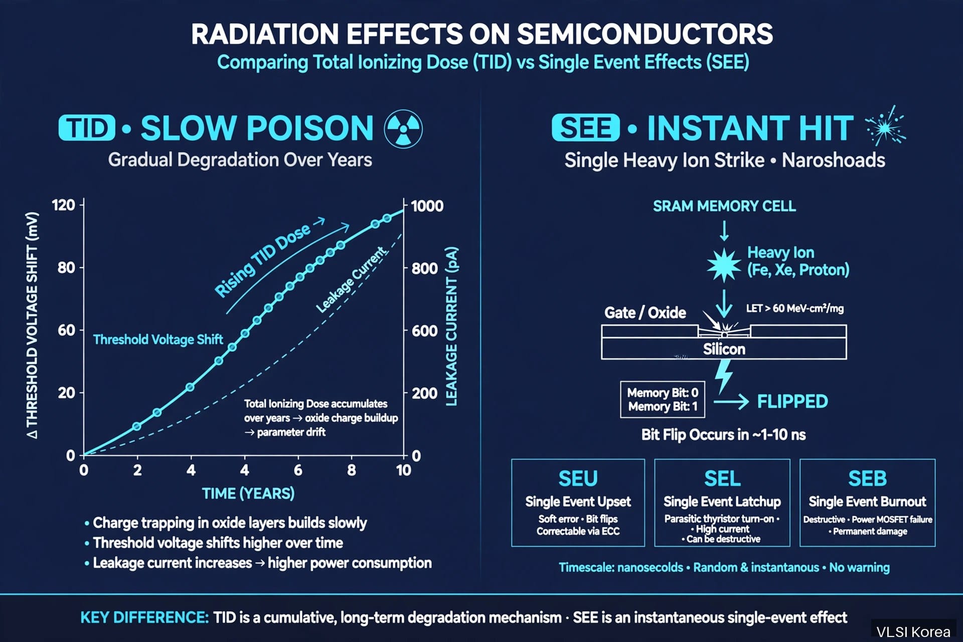
Total ionizing dose is the cumulative energy that ionizing radiation deposits in a material, measured in rad(Si) — dose absorbed in silicon. One rad(Si) is 100 erg per gram. The number itself is small; the accumulation is the problem.
The mechanism runs in four steps. First, a passing particle creates electron–hole pairs in the silicon dioxide that insulates every MOS transistor gate and isolates neighboring devices. Second, electrons are mobile and are swept out quickly, but holes move slowly and a fraction of them get trapped in the oxide, especially near the silicon interface. Third, that trapped positive charge changes the transistor itself: threshold voltage shifts, off-state leakage rises through parasitic edge paths in shallow trench isolation, carrier mobility falls, and low-frequency (1/f) noise increases. Fourth, the circuit drifts — timing margins shrink, standby current climbs, analog offsets wander — until one day the part is out of specification and the mission degrades or ends.
Three properties make TID treacherous for a data center operator. It is cumulative: there is no reboot for oxide charge. It is uneven: two chips on the same board can age at different rates depending on local shielding and bias conditions during exposure. And it is quiet: nothing alarms when a threshold voltage has moved 50 mV; the failure announces itself later, as a timing violation on the hottest day of the mission. A terrestrial data center replaces failed servers in hours. An orbital one watches the same slow failure arrive on schedule, years in advance, with no truck roll possible.
Context for the numbers above: many unhardened commercial parts fail functionally somewhere around 3 to 10 krad(Si), with about 5 krad(Si) a common rule-of-thumb failure point. LEO rad-tolerant parts are typically specified at 20 to 50 krad(Si). Fully rad-hard parts target 100 krad(Si) to 1 Mrad(Si). The gap between a commercial GPU's natural tolerance and a GEO mission's dose is roughly two orders of magnitude — that gap is the entire rad-hard industry.
SEE: one particle, one nanosecond, one dead chip
A single-event effect needs no accumulation. A heavy ion crossing a reverse-biased junction leaves a dense ionization trail; the circuit collects that charge through drift, funneling, and diffusion. If the collected charge exceeds the node's critical charge (Qcrit) — the minimum charge that changes its state — the node flips. Collection takes picoseconds; the upset is decided within nanoseconds. Shielding does not solve this: it filters the low-energy end of the spectrum, while the high-energy ions that cause the worst SEE pass through essentially unaffected. Mitigation has to happen in the device, the circuit, and the system.
| Effect | What happens | Recoverable? |
|---|---|---|
| SEU (single-event upset) | A bit flips in SRAM, a register, or a flip-flop | Yes — correct with ECC, rewrite, or reset |
| SET (single-event transient) | A voltage glitch propagates through logic or an analog chain | Yes — if filtered or captured harmlessly; dangerous if latched |
| SEFI (single-event functional interrupt) | A control block hangs; the device stops responding correctly | Yes — by reset or power cycle, with service interruption |
| SEL (single-event latchup) | A parasitic thyristor turns on and shorts the supply; current runs away | Sometimes — only if current is limited and power is cycled fast; otherwise destructive |
| SEB / SEGR (burnout / gate rupture) | A power MOSFET burns out or its gate oxide ruptures | No — permanent destruction |
Table: the SEE family, ordered from routine to fatal. An ODC design goal is not zero events — it is zero uncorrected, unrecoverable events.
📩 Following this story?
Get the follow-up analysis — earnings, reports and HBM supply — in your inbox daily at 10:30 KST. Subscribe free →
For a compute payload, the arithmetic is unforgiving. A modern accelerator carries gigabits of SRAM and configuration state. Even a tiny per-bit upset cross-section, multiplied by billions of bits and years of exposure, yields a steady rain of flips. Uncorrected, they corrupt model weights, gradients, and checkpoints silently — the worst kind of data center failure, because the output looks plausible. This is why memory architecture, covered in Episode 6, and scrubbing strategy matter as much as the process node.
The scaling paradox: smaller transistors, two opposite effects
Advanced nodes cut both ways. Smaller, thinner oxides trap less TID charge per device, and modern processes are often intrinsically better on total dose than the thick-oxide generations before them. The sensitive volume of each node is also smaller, so a single ion collects less charge in one transistor.
But the critical charge falls faster. At advanced nodes a storage node's Qcrit is on the order of a femtocoulomb or less, because node capacitance and supply voltage have shrunk with scaling. A strike that a 180 nm latch would have shrugged off can flip a FinFET-era register. Charge sharing adds a second problem: one ion track can upset several adjacent cells at once, turning a single-bit error into a multi-bit error that defeats simple ECC unless bits of one word are physically interleaved across the array. GAA (gate-all-around) channels and SOI substrates shrink the collection volume again — helpful, not sufficient. The honest summary as of October 2026: scaling improved TID, complicated SEE, and moved the fight from the process to the architecture.
Rad-hard by design: the five-layer stack
Radiation hardening by process (RHBP) uses special wafers, epitaxy, or SOI substrates. Radiation hardening by design (RHBD) achieves tolerance on a standard process with layout and circuit techniques — and RHBD is what makes modern space silicon economically possible, because it rides commercial foundry capacity instead of a boutique line. In practice the two blend into a five-layer stack.
- Process layer. SOI (silicon-on-insulator) confines each transistor in a dielectric tub, cutting the charge-collection volume and eliminating the classic latchup path. Thin oxides and careful isolation design reduce TID leakage paths.
- Layout layer. Enclosed layout transistors (ELT) wrap the gate around the drain, removing the oxide edge where TID leakage flows. Guard rings surround sensitive devices, sink stray carriers, and break the parasitic thyristor before SEL can sustain itself. Wider spacing between critical nodes limits charge sharing.
- Circuit layer. Hardened storage cells (for example DICE-style dual-interlocked latches) tolerate a strike on one node by construction. Resistive decoupling slows transients so restoring transistors win the race. Triple modular redundancy (TMR) triplicates logic and votes — expensive in area and power, reserved for control paths where a single wrong output is unacceptable.
- Memory layer. ECC (SECDED and stronger chipkill-class codes) corrects flips, bit interleaving spreads one physical strike across many logical words so each word sees only a correctable single-bit error, and background scrubbing periodically reads, corrects, and rewrites memory so errors never accumulate into an uncorrectable pair.
- System layer. Watchdogs, current monitors that detect latchup and power-cycle the affected block in milliseconds, checkpointing, and fault detection, isolation, and recovery (FDIR) software assume events will happen and make them operationally boring.
Every layer charges rent in area, power, performance, or all three. A fully hardened design can cost several times the silicon area of its commercial twin and run generations behind on raw performance — the reason Episode 2 examines how Starlink-class systems instead fly largely commercial silicon behind layers 4 and 5, accepting upsets and engineering the recovery.
Qualification: dose, LET, and the discipline of margin
Rad-hard is a tested specification, not an adjective. TID qualification irradiates biased parts — classically with cobalt-60 gamma sources — to the mission dose multiplied by a radiation design margin, commonly a factor of 2, then re-measures parametrics. SEE qualification exposes parts to heavy-ion beams across a range of LET values and measures the error cross-section versus LET curve, from which on-orbit upset rates are predicted with environment models. A part specified "SEL-immune to 62 MeV·cm²/mg" is making a precise, testable claim: no latchup observed up to that LET. LEO rad-tolerant parts commonly claim SEL thresholds in the roughly 37 to 62 MeV·cm²/mg range and TID of 20 to 50 krad(Si); anything vaguer than numbers like these in a datasheet should be treated as marketing, not engineering.
Displacement damage completes the picture: protons and neutrons knock silicon atoms out of the lattice, shortening carrier lifetime. CMOS logic tolerates it comparatively well; bipolar devices, image sensors, and optoelectronics degrade first — one reason optical intersatellite links (Episode 5) need their own radiation budget.
Chase's Take
From a VLSI seat, the ODC radiation problem is a PPA (performance, power, area) problem wearing a physics costume. Every hardening decision is a trade an engineer can price: TMR triples a block to save a mission; ECC costs bits and bandwidth to buy silent correctness; SOI costs wafer premium to delete a failure class. The winning ODC architectures will not be the ones with the most hardening — they will be the ones that spend hardening exactly where an error is unrecoverable (power devices, boot state, control logic) and buy the rest back with statistics (ECC, scrubbing, redundancy across satellites). A constellation is itself an error-correction code: losing one node is a correctable error if the system was designed to notice. That reframing — chip-level RHBD plus constellation-level fault tolerance — is where the MBA math and the device physics meet, and it decides whether the 10 MW break-even model in Episode 8 survives contact with reality.
Implications
- For ODC operators: orbit selection is a silicon decision. A few hundred kilometers of altitude can multiply mission dose and erase the cost advantage of COTS compute.
- For chip vendors: the datasheet numbers that matter are TID in krad(Si), SEL LET threshold, and SEU cross-section — published, tested, and margined. AI accelerator vendors who publish them first will own the qualification conversation.
- For memory roadmaps: charge-based storage (DRAM, SRAM, flash) is inherently upset-prone; magnetic and resistive memories change the SEE equation, which is why Episode 6 treats memory as the ODC bottleneck.
- For test and EDA: radiation-aware sign-off — upset-rate prediction, charge-sharing analysis, TID drift models — becomes part of the standard flow, not a post-tapeout surprise.
FAQ
What is the difference between TID and SEE?
TID is cumulative damage from total absorbed dose over time: trapped oxide charge shifts transistor parameters until the chip drifts out of specification. SEE is damage or disruption from one particle in one instant: a flipped bit, a hang, a latchup, or a burned-out device. TID is managed with dose budgets and margin; SEE is managed with hardened design, ECC, and recovery.
How much radiation does a chip in low Earth orbit face?
Order of magnitude, a LEO chip behind typical shielding accumulates about 3–5 krad(Si) over 3–5 years near 800 km, rising to about 30–50 krad(Si) near 1,400 km, with most dose arriving during South Atlantic Anomaly passes. GEO missions design for about 100 krad(Si) class over 10–15 years. Exact values require orbit-specific analysis.
Can shielding stop radiation from killing chips?
Only partly. Shielding is effective against electrons and lower-energy protons, so it reduces total dose substantially — going from 5 mm to 10 mm of aluminum can cut a GEO dose from about 100 krad to about 10 krad over 18 years. But high-energy heavy ions pass through practical shielding almost unaffected, so single-event effects must be mitigated in the silicon and the system, not with mass alone.
What does radiation-hardened by design (RHBD) mean?
RHBD means achieving radiation tolerance on a standard commercial process through design techniques — enclosed layout transistors, guard rings, hardened latches, TMR, ECC, interleaving, and scrubbing — instead of a specialized hardened fab process. It is what lets space programs use modern foundry nodes, at the cost of area, power, and engineering effort.
Note: dose and LET figures in this episode are order-of-magnitude design references compiled from public NASA/ESA radiation-effects literature accessed on 23 October 2026; flight hardware decisions require mission-specific analysis and part-level test data.
Series: This is Episode 1 of Space Data Center Semiconductors. Start from the hub, the Orbital Data Center Technical Report, and continue with Episode 2 — the COTS counterattack: how Starlink-class systems keep commercial chips alive in orbit. Related briefings: leo-01 (Starlink chips) and leo-02 (terrestrial GPUs in space), linked from the hub.
📩 Missed today's analysis? Get tomorrow's in your inbox
Daily Silicon at 10:30 KST plus earnings and analyst-report breakdowns, first. Samsung Electronics, SK hynix, TSMC and HBM supply, read by practicing engineers. Join 300+ subscribers.
Subscribe free →
Free · No spam · Unsubscribe anytime