VLSI Korea
Daily Silicon: Semiconductor Design and AI Chips: CoWoS and $3 billion R&D
A practicing semiconductor engineer's daily read on global silicon news - Semiconductor Design and AI Chips: CoWoS and $3 billion R&D


🆓 무료 글 · 누구나 무료로 읽을 수 있는 글입니다
A practicing semiconductor engineer's daily read on global silicon news:
The CoWoS-versus-EMIB choice changes interconnect verification and customer-qualification wait time more than package size, while Lam plans to invest more than $3 billion in its R&D lab network over 5 years and lift experiment capacity by more than 50%.
Chase's Take - From a backend perspective, I care less about whether CoWoS or EMIB wins than about how many wafer splits and measurement turns an engineering change passes through before it reaches customer qualification. More lab throughput does not shorten post-tapeout ramp time if the metrology and reliability queues stay put.
The next check is whether Lam's 50% capacity expansion actually translates into shorter customer-site validation lead time.
1. Advanced Packaging Market Trends: CoWoS and EMIB
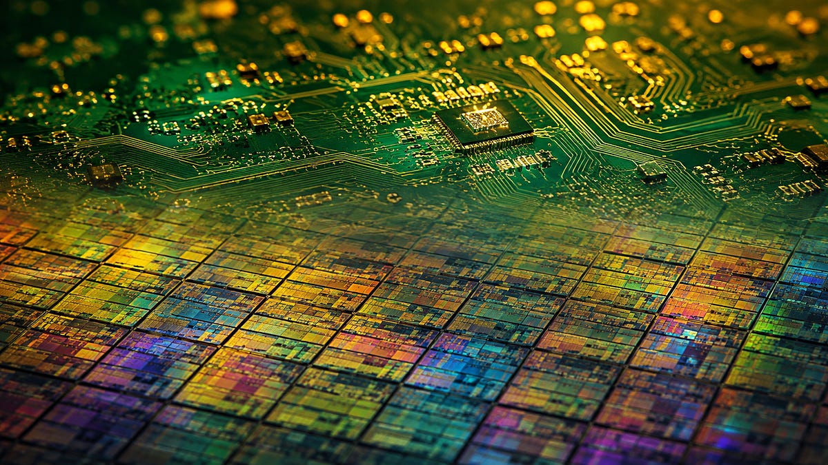
TL;DR - TrendForce treats CoWoS·CoPoS, Intel EMIB, and glass substrates as one advanced-packaging supply-chain problem.
Different interposer structures and reticle-expansion paths shift the comparison from die area to interconnect verification; backend signoff needs substrate, bridge, micro-bump, and test escape in one table.
Source: TrendForce - Advanced Packaging Market Trends: CoWoS and EMIB
2. Lam Global Lab Network: $3 billion R&D

TL;DR - Lam plans to invest more than $3 billion over 5 years to lift R&D lab experiment capacity by more than 50%, supporting more than one million experiments; it says some process-development timelines are up to 2.5x faster.
The ramp gain still depends on shrinking metrology and reliability queues, not tool count.
Source: Lam Research - Lam Global Lab Network: $3 billion R&D
3. Silvaco and Dassault: First-Time-Right Semiconductor Manufacturing

TL;DR - Silvaco and Dassault Systèmes announced a connected digital twin workflow for first-time-right semiconductor manufacturing.
It only changes yield ramp if the model boundary between TCAD/EDA results and fab data, calibration ownership, and release gates are explicit.
Source: Silvaco - Silvaco and Dassault: First-Time-Right Semiconductor Manufacturing
4. SRC Launches SPARC

TL;DR - SRC launched SPARC to consolidate industry-led university research in semiconductor innovation, packaging, and manufacturing.
To reach product PDKs, thermal, power-integrity, reliability, and qualification data need to close in the same loop early.
Source: SRC - SRC Launches SPARC
What to Watch Next
- Lam R&D lab network multi-site expansion schedule
Track whether more than 50% higher experiment capacity converts into shorter customer-qualification lead time. - CoWoS and EMIB reticle expansion and interconnect-yield disclosures
Assess how larger package sizes change substrate, bridge, and test-coverage constraints. - Calibration scope of the Silvaco-Dassault digital twin workflow
See whether traceability between models and fab data actually feeds into yield ramp. - SRC SPARC's first solicitation and industry-sponsor scope
See whether packaging research reaches the PDK and reliability handoff.
Signal Radar — More Headlines
- SIA Names Michael Robbins President and CEO (Semiconductor Industry Association)
- ITM Semiconductor H1 Revenue Excluding Apple (The Elec)
- [AI Ecosystem] The Paradigm Shift in AI Computing (SK hynix)
Further Reading on VLSI Korea
- VLSI Korea Calendar (2026-08-17): Semiconductor Jobs, Industry Events, and Education
Useful background for today's brief. - What Semiconductor Sales Teams Do: EDA, Equipment, IDM, and Fabless Workflows
Useful background for today's brief.