VLSI Korea
Why Hybrid Bonding Is Hard to Perfect: The Yield War Behind 16-High HBM
Hybrid bonding is mandatory for 16-high HBM, but volume yields are not solved. Overlay under 0.3um, CMP recess under 2.5nm, and particle control form a triple wall. Samsung targets partial HBM4E adoption; SK hynix points to HBM5. The longer the delay, the longer the TC bonder moat holds.


The 30-Second Summary
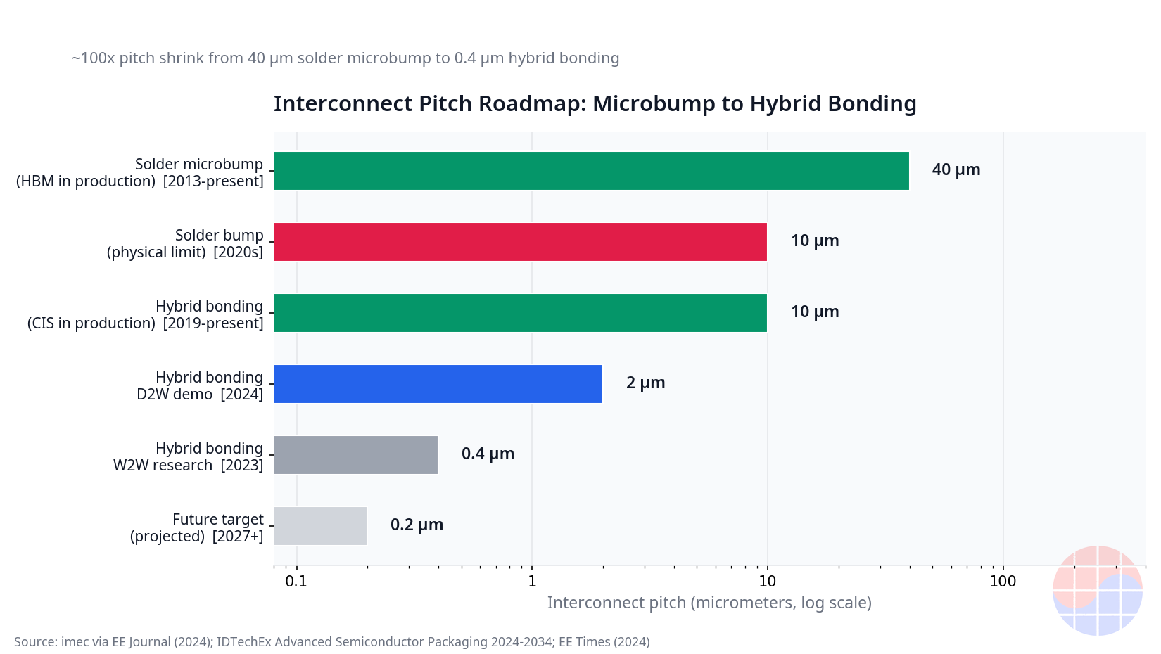
The bottom line first: hybrid bonding is a necessary condition for the 16-high HBM era, but it is not yet a sufficient one for volume production. It is a bumpless 3D stacking technology that joins copper pads directly, shrinking interconnect pitch from roughly 40µm with solder microbumps to under 10µm (0.4µm in research). The catch is yield. Three stacked walls stand in the way: overlay accuracy below 0.3µm, CMP control holding copper recess under 2.5nm, and particle-plus-anneal warpage discipline. Stick to confirmed facts: Samsung Electronics disclosed HBM4-based HCB (Hybrid Copper Bonding) sample shipments on its January 2026 earnings call, and SK hynix's official August 2026 tech note points to a transition at the HBM5 generation. In other words, "hybrid bonding is locked in for 16-high HBM4E" is still a hypothesis, not a fact. The investor read is simple: the longer the transition takes, the longer the TC bonder incumbent's moat holds; the faster it arrives, the sooner power shifts to the European and Japanese bonder makers.
Background: Why Hybrid Bonding Matters Right Now
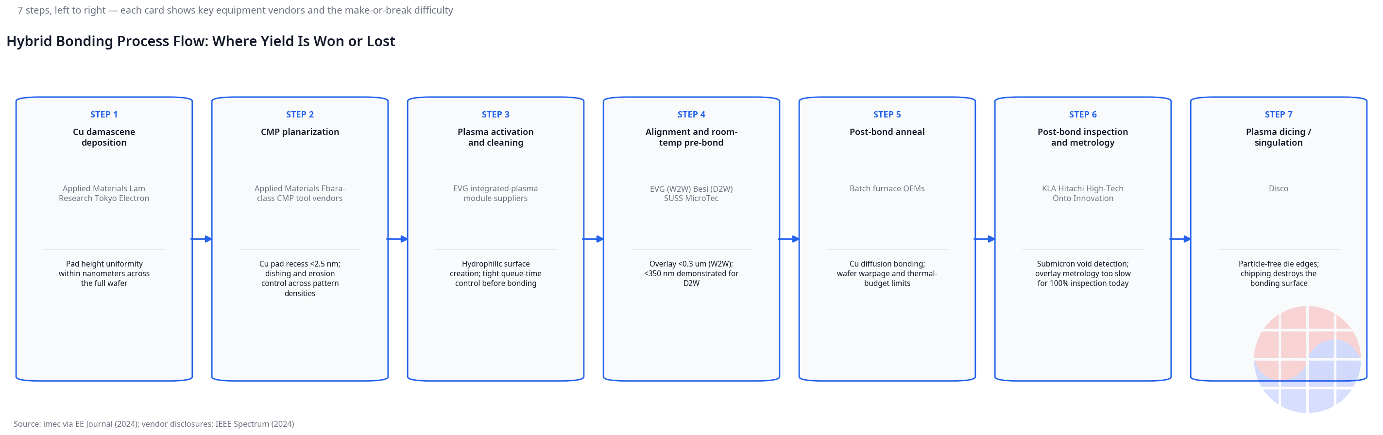
Hybrid bonding fuses dielectric to dielectric and copper to copper in a single step, also known as DBI (Direct Bond Interconnect). The recipe reads simply: form copper damascene wiring, planarize with CMP to near-atomic flatness, activate the surface with plasma, pre-bond at room temperature via hydrogen bonds, then anneal to complete copper diffusion bonding. No solder anywhere. The thickness added per layer collapses from 10–30µm with microbumps to 1–2µm.
Image sensors have shipped with this technology since 2019. So why is the memory industry suddenly obsessed? The answer sits in the HBM4 specification sheet. As SK hynix laid out in its August 2026 tech note, HBM4 doubles I/O from 1,024 in HBM3E to 2,048, pushes stack height toward 16 layers and beyond, and keeps the package height ceiling fixed at 775µm. Try building that with TC bonders and microbumps and three things break at once. First, tens of microns of bump thickness times 16 layers blows past the height budget. Second, CTE mismatch accumulates alignment error across 16 layers. Third, the underfill between bumps becomes the thermal bottleneck.
That is why hybrid bonding looks less like an option and more like a prerequisite. At NVIDIA GTC in March 2026, Samsung showed HCB supporting stacks of 16 or more layers with thermal resistance down more than 20% versus conventional TC bonding. At the Future of Memory and Storage conference in Santa Clara in August 2026, Samsung unveiled its zHBM concept, stacking HBM directly on top of AI accelerators. Samsung's 3D DRAM roadmap points the same way: per market reports, the company showed a 16Gb prototype combining a 4F² cell with wafer-to-wafer (W2W) hybrid bonding at ISSCC in February 2026, targeting commercialization around 2028. SK hynix's CTO stated at the 2025 IEEE VLSI Symposium that the company's 4F² VG (Vertical Gate) platform and 3D DRAM would target sub-10nm nodes.
Step back, though. A technology being necessary is a different claim from yields being ready.
Interlude: W2W, D2W, D2D — Three Ways to Bond
Hybrid bonding splits three ways depending on what gets bonded to what. W2W (wafer-to-wafer) bonds whole wafers at once. Fast and simple, but there is no way to screen out bad dies — the compound yield is the product of both wafers' yields. D2W (die-to-wafer) bonds only pre-tested good dies onto a wafer. KGD (known-good-die) screening is possible, but pick-and-place speed is the bottleneck. D2D (die-to-die) bonds die to die, mostly for chiplet combinations. Image sensors won with W2W; logic chiplets use a mix of D2W and D2D. Sixteen-high HBM — large dies, many layers — is the one arena where no option can yet claim to be the answer.
Why Memory Is the Hardest Application
Logic chiplets with hybrid bonding are already in volume production. Memory, and HBM in particular, lags for three reasons. First, die area is large: bigger dies amplify warpage and particle exposure. Second, layer count is extreme: logic typically bonds two layers; HBM targets sixteen. Third, cost sensitivity is brutal. Logic chiplets are high-margin products that can absorb an expensive process; memory is a cost-per-bit business where one point of yield goes straight to unit cost. The bar for memory hybrid bonding is set far higher than anywhere else.
Deep Dive: Why It Is Hard — Seven Walls
1. Overlay: a nanometer war
The alignment spec for hybrid bonding is brutal. Industry analysis puts microbump alignment at 3–10µm; hybrid bonding demands under 0.3µm (300nm). W2W lives in the hundreds-of-nanometers regime, and die-to-wafer (D2W) is tougher still. imec's 2024 demonstration hit 2µm pitch with D2W overlay error under 350nm and Kelvin electrical yield above 85%. That sounds impressive until you invert it: even at 2µm pitch, the error budget is only a few hundred nanometers. In a 16-high stack, that error compounds layer by layer. One finished product needs fifteen bonding interfaces to all succeed, not one.
2. CMP: fighting 2.5nm of recess
If the step between copper pads and the dielectric surface exceeds 2.5nm, the bond fails. That was exactly imec's demo condition. CMP must control dishing (copper polishing faster than dielectric) and erosion (pattern-density-dependent polish rates) across the entire wafer at nanometer scale — a tougher spec than front-end CMP. Annealing lets copper expand into contact, but oversized initial recess leaves voids behind.
3. Plasma activation and queue time
Surfaces must be rendered hydrophilic by plasma just before bonding so that room-temperature pre-bonding takes hold. The catch: activated surfaces have a shelf life. Miss the queue-time window between activation and bonding and bond strength collapses. It is a hidden tax on fab scheduling flexibility.
4. Particles: one speck is a killer defect
Hybrid bonding wants Class 100 cleanroom assembly. A single submicron particle trapped at the interface becomes a void, and that die is scrap. imec went as far as adopting plasma dicing to keep singulation particle-free. From a yield-management view, particle control is an operations problem rather than an equipment problem, which makes it harder, not easier.
5. Anneal: heat it without warping it
Pre-bonding relies on weak hydrogen bonds, so a high-temperature anneal must drive the interface to full covalent bonding before downstream processing. But warped wafers stress the bond line. The thinner the dies — tens of microns in memory stacks — the more warpage control degrades with each added layer. Thermal budget bites too: copper must diffuse at temperatures that do not damage the devices underneath.
6. Throughput versus yield: the W2W–D2W dilemma
W2W bonds the whole wafer at once, so it is fast — but there is no way to screen out bad dies, and the compound yield is the product of both wafers' yields. D2W bonds only known-good dies (KGD) but pick-and-place speed is the bottleneck. The industry has not settled which route fits memory. Image sensors won with W2W, but stacking sixteen large-area DRAM dies has no precedent.
The Equipment Map: Who Makes Money, and Where
The hybrid bonding equipment market has different winners at each process step.
In bonders, two camps dominate. EVG is the established W2W leader, carrying its fusion-bonding installed base into hybrid bonding. In D2W, the Netherlands' Besi leads; its investor-day disclosures put cumulative hybrid bonder orders in the triple digits, with the current customer mix skewed toward logic. SUSS MicroTec and ASMPT hold positions across both W2W and D2W.
CMP belongs to Applied Materials and fellow CMP tool vendors; post-bond inspection and metrology sits with KLA, Hitachi High-Tech, and Onto Innovation. Detecting submicron voids at the bond interface is still too slow for 100% inline inspection — a bottleneck that, read differently, is an open opportunity for metrology vendors.
This is where Korean investors should pay attention. Today's HBM packaging runs on TC bonders, and that world belongs to Hanmi Semiconductor. Per TechInsights data cited in February 2026, Hanmi holds 71.2% of the HBM TC bonder market. Founded in 1980 and headquartered in Incheon, the company has been the prime beneficiary of every Samsung and SK hynix HBM capacity cycle. The longer the hybrid transition takes, the longer this moat lasts.
If the transition accelerates, the beneficiary axis shifts. SEMES, Samsung's equipment affiliate, is developing a W2W hybrid bonder (reported February 2026). Hanwha Semitech has reportedly sent second-generation hybrid bonder samples to SK hynix. Samsung is reported to be building a D2W hybrid bonding production line at Pyeongtaek P5 (reported July 2026). To be explicit: these are press reports, not company-confirmed facts. Even so, the direction is legible. The three memory makers are hedging between buying hybrid bonders abroad and cultivating them at home.
Chase's Take: This Is a Timing Problem, Not a Technology Problem
Through an engineer's lens, the difficulty of hybrid bonding converges on one equation. The compound yield of a 16-high stack is the per-interface yield raised to the 15th power. At 99% per interface, fifteen multiplications leave 86%. At 95%, you get 46%; even at 99.5%, only 93%. Just as an STA engineer stacks timing margins layer by layer, a packaging engineer must beat this multiplicative curse. The volume-manufacturing gate is therefore not "does it work" but "at what stable percentage."
Through an MBA lens, the most interesting fact is that the two Korean makers quote different schedules for the same technology. Samsung's January 2026 earnings call spoke of "partial commercialization of selected products" at the HBM4E stage. SK hynix's August 2026 tech note points to a transition at HBM5. If yields were solved, there would be no reason for the schedules to diverge. The gap between them is the current state of yield, expressed in calendar quarters.
For investors, read the gap this way: hybrid bonding insertion in 16-high HBM4E is a contested hypothesis. On June 18, 2026, SK hynix shipped 12-high HBM4E samples (48GB, 16Gbps per pin) to major customers — packaged with Advanced MR-MUF, not hybrid bonding. The mainstream packaging story for the HBM4E generation is still an extension of incumbent technology. The fact-based bet on hybrid bonding sits on the HBM5 (20-high and above) timeline.
The equipment investment thesis reduces to a binary. Scenario A (delayed transition): Hanmi Semiconductor's TC bonder moat holds, and the fruits of HBM4/HBM4E capacity expansion flow to the incumbent. Scenario B (accelerated transition): power migrates to Besi, EVG, and SUSS, while a share battle opens among domestic options like SEMES and Hanwha Semitech. Neither scenario is bad for Korea: scenario A favors Hanmi, scenario B brings SEMES and Hanwha Semitech into the frame. The real risk is the third scenario — no transition and no capacity expansion — which only happens if AI memory demand itself breaks.
Implications: What Investors and Executives Should Track
1. Hybrid bonding in 16-high HBM4E is unconfirmed. Treat "it will be adopted" reporting as hypothesis. Anchor only on official statements: Samsung's January 2026 earnings call and SK hynix's August 2026 tech note.
2. The yield-stabilization date decides 2027–2028 HBM share. Whoever stabilizes 16-high yields first takes the margin pool of high-stack HBM4E and HBM5. Track the tone of HCB and hybrid bonding mentions across quarterly earnings calls.
3. The equipment watchlist has four branches. ① The TC bonder moat: Hanmi Semiconductor (71.2% share, TechInsights). ② Hybrid bonders: Besi (D2W), EVG (W2W), SUSS. ③ Domestic options: SEMES, Hanwha Semitech. ④ Inspection and metrology: KLA and peers — a process that cannot be fully inspected inline structurally grows metrology demand.
4. 3D DRAM (circa 2028) is the next CAPEX wave. If Samsung's 4F² plus W2W hybrid bonding roadmap materializes, memory equipment spending shifts toward packaging once more. W2W bonders, CMP, and post-bond inspection form the beneficiary chain.
FAQ
Q1. What is the difference between hybrid bonding and conventional TC bonding? TC (thermal compression) bonding presses solder microbumps together with heat and force. Hybrid bonding joins copper pads directly with no solder, while simultaneously bonding dielectric to dielectric. Bump pitch falls from roughly 40µm to under 10µm, and per-layer thickness growth drops from 10–30µm to 1–2µm. The price is alignment precision tightening more than 10x, from 3–10µm to under 0.3µm.
Q2. Is hybrid bonding confirmed for 16-high HBM4E? No. Samsung guided "partial commercialization of selected products" at the HBM4E stage on its January 2026 earnings call; SK hynix's August 2026 tech note points to a transition at HBM5. SK hynix's 12-high HBM4E samples shipped in June 2026 use Advanced MR-MUF packaging. Hybrid bonding in 16-high HBM4E remains a contested industry forecast, not a confirmed fact.
Q3. Why won't yields come easily? Four difficulties multiply: ① overlay accuracy under 0.3µm, ② CMP control holding copper recess under 2.5nm, ③ cleanroom discipline where one particle is a killer defect, and ④ warpage control through anneal. In a 16-high stack, fifteen bonding-interface yields multiply together, so even 99% per interface leaves 86% overall.
Q4. Which equipment makers should Korean investors watch? It depends on timing. A delayed transition preserves Hanmi Semiconductor's moat at 71.2% of HBM TC bonders (TechInsights). An accelerated transition shifts the benefit toward hybrid bonder makers Besi, EVG, and SUSS, and opens a share contest among domestic options SEMES and Hanwha Semitech. Post-bond inspection and metrology (KLA and peers) is a structural beneficiary either way, since the process resists full inline inspection.
Footnote: the 2029–2030 volume-production timelines, the Pyeongtaek P5 D2W line build, and Hanwha Semitech's sample shipments to SK hynix cited above rest on press reports and are not company-confirmed. Samsung's HCB sample shipments and HBM4E partial-commercialization plan come from its January 2026 earnings call; SK hynix's HBM5 transition signal comes from its August 2026 official tech note. All figures reflect public disclosures as of October 14, 2026.