VLSI Korea
DRAM Without a Capacitor — Vertical Dual-Gate IGZO Reaches 4F2 in a 2T0C Cell
A capacitor-less 2T0C DRAM cell reaches the 4F2 floor. A number-by-number dissection of the CAS vertical dual-gate IGZO result, honestly compared with the Samsung and SK hynix silicon 1T1C 4F2 route: 470 s retention, and the 90 s limit at 85 C.


Start with the conclusion. Remove the capacitor and a DRAM cell can reach 4F2, the smallest footprint the notation allows. A team led by the Institute of Microelectronics at the Chinese Academy of Sciences has now demonstrated exactly that, forming two vertical dual-gate IGZO transistors in a single self-aligned etch. The best cell held data 1 for 350 to 470 seconds and data 0 for more than 500 seconds, and stored 4 bits per cell. The caveats matter just as much: this is a single-cell demonstration, retention falls to 90 seconds at 85 C, and no endurance data is reported. It also shares only a name with the silicon 1T1C 4F2 programs at Samsung Electronics and SK hynix. The physics is entirely different. This article dissects the paper number by number and puts both routes on the same table.
Source paper: Liao et al., High-density three-dimensional integration of dynamic random-access memory using vertical dual-gate IGZO TFTs, Nature Communications 16:10932 (2025). DOI: 10.1038/s41467-025-65925-3. Preliminary results appeared at IEDM 2024. Affiliations: Institute of Microelectronics, Chinese Academy of Sciences, Beijing; Beijing Superstring Academy of Memory Technology; Darwin College, Cambridge; Shandong University.
Why the capacitor is the problem
Conventional DRAM is 1T1C: one transistor plus one capacitor. Cell area is written as a multiple of F squared, where F is the minimum feature size. The industry has been stuck at 6F2 for more than a decade.
The blocker is not the transistor. It is the capacitor. Holding enough charge forces the capacitor into a tall, narrow pillar. Shrink the cell to 4F2 and the pillars stand too close together: leaning, interference and extreme aspect ratios follow. That geometry is the structural ceiling of 1T1C.
A 2T0C cell removes the premise. There is no separate capacitor. The gate oxide capacitance of the read transistor itself serves as the storage node: two transistors, zero capacitors. IGZO is the channel material for three reasons. Its wide bandgap gives an extremely low off-current. It can be processed near 250 C, which fits back-end-of-line integration on top of logic. And charge leaks so slowly that refresh intervals can stretch by orders of magnitude.
Three things this paper actually does differently
1. SASS: both transistors in one step
Conventional vertical stacking builds the write and read transistors layer by layer. Any offset between layers becomes misalignment, and misalignment is paid for in area.
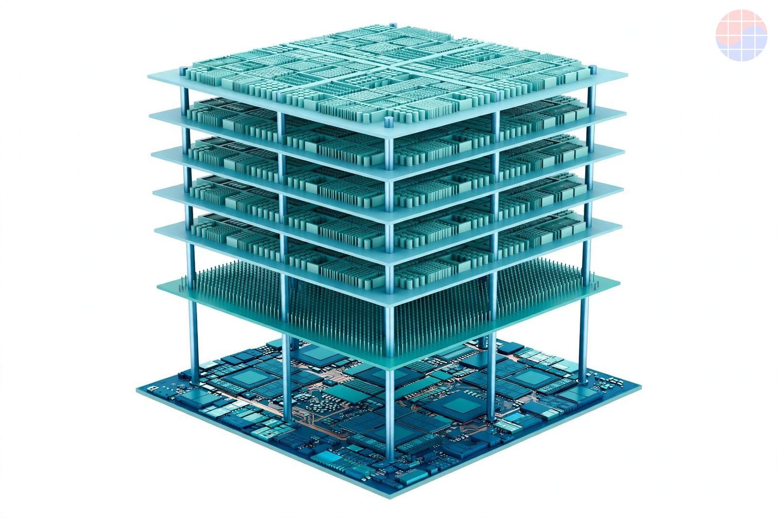
SASS stands for Self-Aligned Single-Step. Five electrode layers and four isolation layers are deposited first, then a single etch opens the circular channel and forms both transistors at once. ITO at 30 nm serves as ground, bit line and storage node. Ta at 40 nm serves as the read and write word lines. The isolation layers are 40 nm SiO2.
The payoff is direct. Photolithographic misalignment is removed by construction. Cross-section TEM at a critical dimension of 150 nm shows no observable offset between the top and bottom devices. Fewer steps also mean fewer thermal cycles and fewer contamination opportunities.
2. Vertical dual gate: from 20F2 planar to 4F2
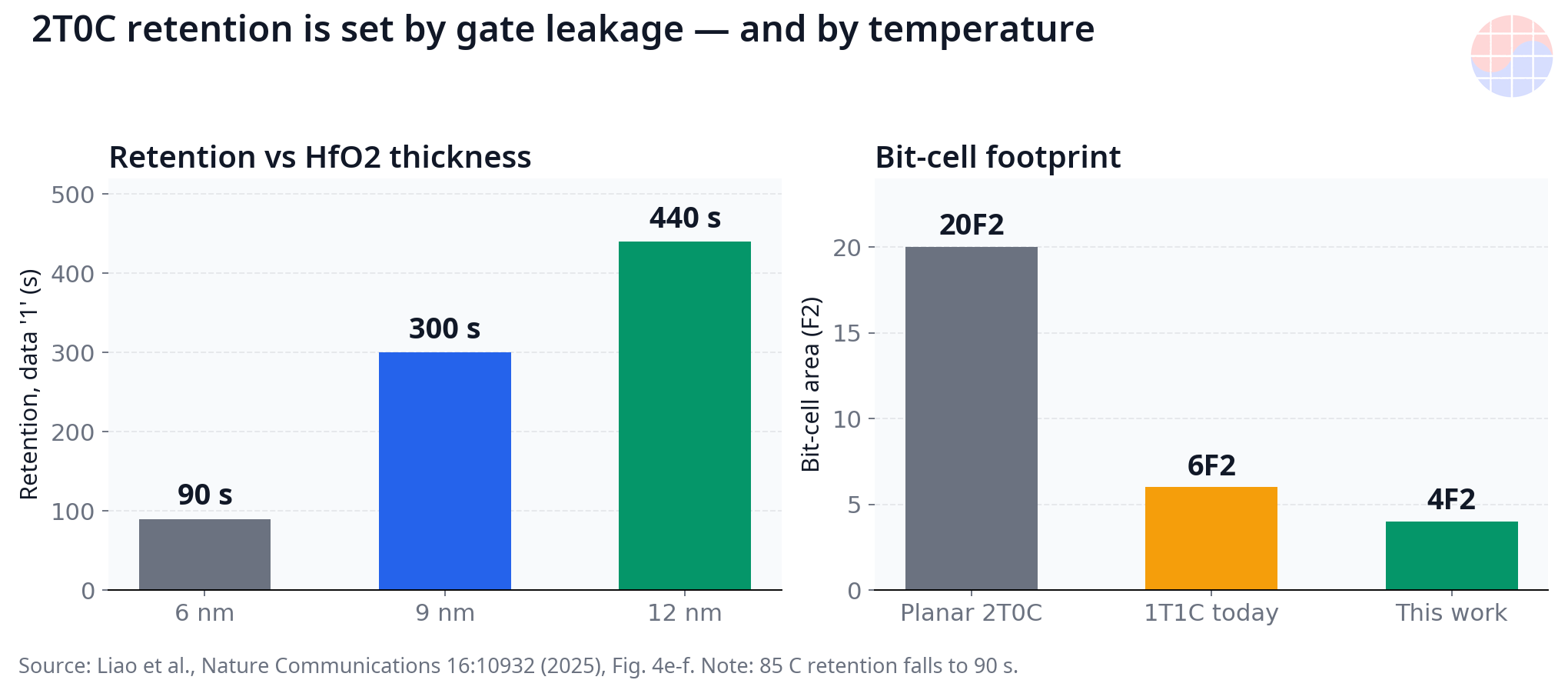
A planar 2T0C cell occupies about 20F2. By standing the channel up and gating it from both sides, this work reaches 4F2, the minimum the area notation permits.
The dual gate is not only about area. It makes the read operation more reliable, hardening the cell against the current-sharing and IR-drop problems of single-gate reads. The extra gate on the write transistor also adds storage-node capacitance, which means more stored charge. The price is the hold bias: that same extra capacitance forces the write word line to minus 1.5 V to keep the write transistor firmly off.
3. In-situ ozone self-oxidation: grow the dielectric in place
The Ta metal gate is oxidized by ozone inside the same ALD chamber to form the high-k dielectric Ta2O5 directly. Conditions are 250 C for 45 minutes to one hour. The resulting film is 7 nm thick, with a dielectric constant near 21 and a breakdown field of 5 MV/cm.
Staying in one chamber is the point. Compared with ex-situ oxygen oxidation, interface contamination falls and uniformity improves. The channel stack, IGZO 6 nm, HfO2 9 nm and IZO 25 nm, is deposited by PEALD in the same chamber. Sputtered IGZO showed thickness variation above 1.5 nm; PEALD IGZO held variation near 0.3 nm. In a vertical channel, that difference shows up directly as current spread.
Device performance, in numbers
Best-device figures use a channel length of 120 nm and a width-to-length ratio of 500 nm to 120 nm.
| Metric | Best device | Statistics (24 devices, in-situ) | Why it matters |
|---|---|---|---|
| Subthreshold swing SS | 63 mV/dec | 68 +/- 5 mV/dec | Close to the 60 mV/dec theoretical limit |
| On-current Ion | 50.3 uA/um | 45 +/- 5 uA/um | At Vgs = Vth + 1 V, Vds = 1 V |
| Threshold voltage Vth | -0.04 V | Near zero | Tunable through the dual gate |
| Transconductance Gm | Above 100 uS/um | - | Supports a usable read current |
| CD scaling | 6 um down to 100 nm | No Ion or SS degradation | Evidence the vertical structure scales |
Reliability is strong for a vertical-channel device. Under positive bias temperature stress at 85 C, plus 2 V for 3600 s, the threshold shift was 87.7 mV. Under negative stress at minus 2 V it was minus 22.6 mV. Both are better than reported vertical CAA and GAA references. A 30-minute anneal in nitrogen at 300 C left the transfer curves nearly unchanged, which is what BEOL compatibility requires.
Cell operation and retention: the table that counts
Writes use a write word line of 0.5 V, with the bit line at 1 V for data 1 and 0 V for data 0. Reads bias the read word line at 0.5 V and sense current at a bit-line voltage of 0.1 V. The stored-current ratio exceeds 300.
| Item | Value | Condition and caution |
|---|---|---|
| Data 1 retention, best | 470 s | Representative Fig. 4 cell. Abstract and Fig. 4b quote 350 s under different conditions |
| Data 1 retention, average | 230 s | Nine cells, all above 100 s |
| Data 0 retention | Above 500 s | Held to the limit of the measurement window |
| Write speed | No decay down to 50 ns | The paper also discusses 10 ns potential. The measured floor is 50 ns |
| Retention at 85 C | 90 s | Down from 410 s at room temperature. Thermally activated carriers are the cause |
| Multi-bit | 4 bits per cell, 16 states | Data voltage 0.2 V to 0.95 V in 0.05 V steps. Read current scales linearly |
Retention is set by two leakage paths: the off-current of the write transistor and gate leakage at the storage node. Thickening HfO2 cuts the gate leakage and stretches retention. At 6 nm retention was 90 s, at 9 nm it was 300 s, and at 12 nm it was 440 s, while total leakage fell from 4.42e-16 A/um toward 4e-17 A/um. In other words, retention here is a gate-stack design variable, not a fixed material limit. That is the engineering message of the paper.
Crosstalk was checked in SPICE, covering Row Hammer and passing-gate effects. Unselected-cell current stayed below 1 fA, while the selected cell separated cleanly at 3.8 uA for data 1 versus 0.2 uA for data 0. Read that correctly: it is simulation, not a large-array measurement.
Multi-bit needs the same discipline. Four bits per cell invites a simple division, effective density equals 4F2 divided by four. That arithmetic is ours, not a claim by the paper, and it should not be quoted as one. Storing analog voltage levels on a storage node is exposed to noise, device variation and temperature. Separating 16 states in one cell and separating them without errors across a full array are different problems.
📩 Following this story?
Get the follow-up analysis — earnings, reports and HBM supply — in your inbox daily at 10:30 KST. Subscribe free →
Honest comparison with imec: where it wins, where it does not
Imec originated the 2T0C concept. In 2020 it reported retention above 400 s with an extracted off-current of 3e-19 A/um. In 2021 it reported gate-length scaling to 14 nm and endurance above 10 to the power of 11 cycles. Planar reports above 1000 s also exist.
| Axis | This work, vertical dual gate | Imec and planar prior art | Verdict |
|---|---|---|---|
| Cell area | 4F2, vertically stacked | About 20F2 planar | This work leads |
| Retention among vertical devices | Up to 470 s, average 230 s | Roughly 10x below this work | Best reported for vertical 2T0C |
| Absolute retention including planar | 470 s | Reports from above 400 s to above 1000 s | Still behind on absolute value |
| Endurance cycles | Not reported | Above 10 to the power of 11 reported | No comparison possible. A gap |
| Process temperature | 250 C BEOL | Low-temperature BEOL capable | Comparable |
| Multi-bit | 4 bits demonstrated | Multi-bit also reported | Comparable |
The contribution is area and integration, not a retention record. This paper shows that standing the cell up does not have to destroy retention. That is a narrower and more credible claim than a headline about beating planar DRAM.
Industry context: same 4F2, different physics
Timing makes this paper land in the middle of a live strategy split. On October 22, 2026, Electronic Times Korea mapped the diverging 4F2 routes across the United States, Korea and China. The essentials are below.
| Player | 4F2 route | Channel and storage |
|---|---|---|
| Micron | Declined 4F2 on cost and complexity. Extends 6F2 and goes to wafer bonding and 3D DRAM | Silicon 1T1C retained |
| Samsung Electronics | Head-on. About five years of prior research. Vertical channel transistors, IGZO materials research and wafer bonding | Silicon-led 1T1C, capacitor retained |
| SK hynix | Head-on. 4F2 vertical-gate platform with wafer bonding, plus a long-term two-track move to 3D DRAM | Silicon-led 1T1C, capacitor retained |
| CXMT | Uses 4F2 to cut area even on ArF tools, routing around EUV restrictions | Silicon-led 1T1C |
| This paper, CAS | Detour. Deletes the capacitor itself to reach 4F2 | IGZO 2T0C, no capacitor |
The Korean 4F2 fight keeps the capacitor and stands only the transistor up. This paper deletes the capacitor. The target area is identical and the bottlenecks are not. The first route is limited by capacitor spacing, aspect ratio and bonding yield. The second is limited by retention, temperature behavior and sensing margin. If one route wins, it does not prove the other was wrong. They bought different risks.
The geopolitics are part of the story. This result comes from a Chinese state research institute. Any density path that does not depend on EUV carries strategic weight under export controls. CXMT pursuing 1T1C 4F2 and this team pursuing 2T0C 4F2 are different answers to the same pressure: raise density without leading-edge exposure tools.
The SK hynix 3D DRAM link, without the hype
At SEDEX 2026, SK hynix projected AI infrastructure scale in 2030 at roughly 20 times the 2026 level, and put two ideas beyond HBM on the roadmap: 3D Stacked DRAM, with DRAM placed directly on the processor, and NAND-based HBF, High Bandwidth Flash.
The BEOL monolithic 3D approach in this paper is legitimately one device candidate for that 3D DRAM picture. Building memory at 250 C after the logic is finished matches the idea of stacking DRAM on a processor.
Hold the line there. The SK hynix roadmap 3D DRAM may well mean stacked 1T1C. A roadmap slide does not fix the channel material or the cell structure. Treating this paper as proof of the SK hynix roadmap would be an overclaim. It is evidence about candidate maturity, nothing more.
Limitations: what this paper does not prove
First, scale. This is a single-cell and small-device demonstration, not a large-array manufacturing demonstration. Yield, variation, defective-cell handling and redundancy are separate and harder problems. Second, endurance. There is no cycling data, which stands out next to the imec figure above 10 to the power of 11 cycles. Third, temperature. Retention collapses to 90 s at 85 C, so the refresh-power advantage erodes quickly in hot operating environments such as servers and automotive. Fourth, dimensions. Demonstrated critical dimensions are 100 to 150 nm, while production DRAM works with F near the 10 nm class. 4F2 is a structural area figure, not a statement that 10 nm-class density has been achieved today. Fifth, multi-bit. Analog voltage storage is fragile against noise and variation, and the error-correction burden can eat the density gain. Sixth, context. With authors at a Chinese state institute, technology transfer and export-control framing will follow this topic regardless of the technical merit. Adoption paths will be shaped by geopolitics as well as by device data.
On manufacturability, neither route is finished. Samsung and SK hynix still face capacitor processing and bonding yield in 1T1C 4F2. This 2T0C route still faces refresh, sensing margin and high-temperature behavior. On sensing alone, a stored-current ratio above 300 looks comfortable in one cell and thins out fast once array parasitics and variation are included.
Investment read: the map without the hype
The firmest beneficiaries are the ones both routes need. Atomic layer deposition and high-aspect-ratio etch tools gain importance in 1T1C 4F2 and in 2T0C 4F2 alike. High-k materials such as HfO2 and Ta2O5, and IGZO precursors, sit in the same position.
BEOL integration also expands the design problem. Memory on top of logic turns thermal design, power integrity and timing analysis into three-dimensional work, which points to more EDA and thermal simulation demand. What to avoid is the single-structure bet. Nothing in this paper justifies moving an IGZO DRAM mass-production date forward on its own.
Outlook: what to watch next
Three checkpoints decide whether this detour becomes a road. First, arrays: a follow-up reporting retention distributions and sensing margin on arrays of at least several kilobits. Second, endurance: cycling data reported together with high-temperature retention, so a like-for-like comparison with imec becomes possible. Third, scaling: holding Ion and SS while pushing the critical dimension below 50 nm is what would validate the density story.
Until those arrive, the precise status of this work is the most convincing demonstration yet of a specific trade: deleting a 40-year constraint, the capacitor, in exchange for new constraints in retention and temperature, now quantified in a vertical 4F2 cell. That is enough to make it worth reading closely, and not enough to call it a production technology.
Frequently asked questions
Q. What is a 2T0C DRAM cell?
A. A DRAM cell built from two transistors and zero capacitors. The gate oxide capacitance of the read transistor serves as the storage node instead of a separate capacitor. Source: Liao et al., Nature Communications (2025).
Q. Why does 4F2 matter?
A. It is the smallest structural cell area in F-squared notation. Production DRAM remains at 6F2. Note that 4F2 describes structure area, not the process node itself.
Q. Is the retention in this paper a world record?
A. No. It is the best level reported for vertical-device 2T0C, but planar 2T0C reports above 1000 s are higher. Best 470 s, average 230 s, and 90 s at 85 C.
Q. How does this differ from the Samsung and SK hynix 4F2 programs?
A. The Korean programs keep the capacitor in a silicon 1T1C cell and stand the transistor up. This work uses IGZO and deletes the capacitor. Same 4F2 label, completely different bottlenecks.
Q. Does 4 bits per cell mean four times the density?
A. Sixteen states were separated in a single cell. Array-level noise, variation and error correction are not in that simple division, and the paper does not claim four times the density.
Q. Is this ready for mass production?
A. No. It is a single-cell level demonstration with no endurance data and no large-array data. Read it as a device candidate for BEOL 3D DRAM.
Sources: Liao et al., Nature Communications 16:10932 (2025), https://www.nature.com/articles/s41467-025-65925-3, DOI 10.1038/s41467-025-65925-3. Imec 2T0C prior work (IEDM 2020, 2021). Electronic Times Korea 4F2 report (2026-10-22). SK hynix SEDEX 2026 keynote reports (2026-10-14).
📩 Missed today's analysis? Get tomorrow's in your inbox
Daily Silicon at 10:30 KST plus earnings and analyst-report breakdowns, first. Samsung Electronics, SK hynix, TSMC and HBM supply, read by practicing engineers. Join 300+ subscribers.
Subscribe free →
Free · No spam · Unsubscribe anytime