VLSI Korea
Tesla Terafab Schedule: 2027 Test Chip, 2028 Volume Production - 7 Features of the World's Largest Chip Fab
Tesla and SpaceX Terafab schedule: a first SRAM test chip in Austin in May-June 2027 and volume production at Gibbons Creek in Q3-Q4 2028 on Intel 14A, with logic, memory, and packaging under one roof.


Key Summary
1. Tesla and SpaceX's semiconductor fab, Terafab, now has calendar dates for the first time. The target is a first SRAM test chip at the Austin research fab in May-June 2027, and volume production at the main Gibbons Creek fab in Q3-Q4 2028. (SpaceX Q3 call on October 20, 2026, Tesla Q3 call on October 21, 2026)
2. This is not an ordinary fab. It puts design, logic manufacturing, memory manufacturing, advanced packaging, and test under one roof, serves only Tesla and SpaceX internal demand with no external customers as a captive fab, and supplies its own power and water.
3. The process at its core is Intel 14A. This is not an in-house process but a structure that brings in Intel technology, so half of the success conditions depend on how fast Intel 14A matures.
4. Musk himself cited a "large error bar" and called it a "crazy fast timeline by semiconductor standards." The real gate is not the building schedule but the yield schedule.
The Schedule Is Out: Test Chip in 2027, Production in 2028
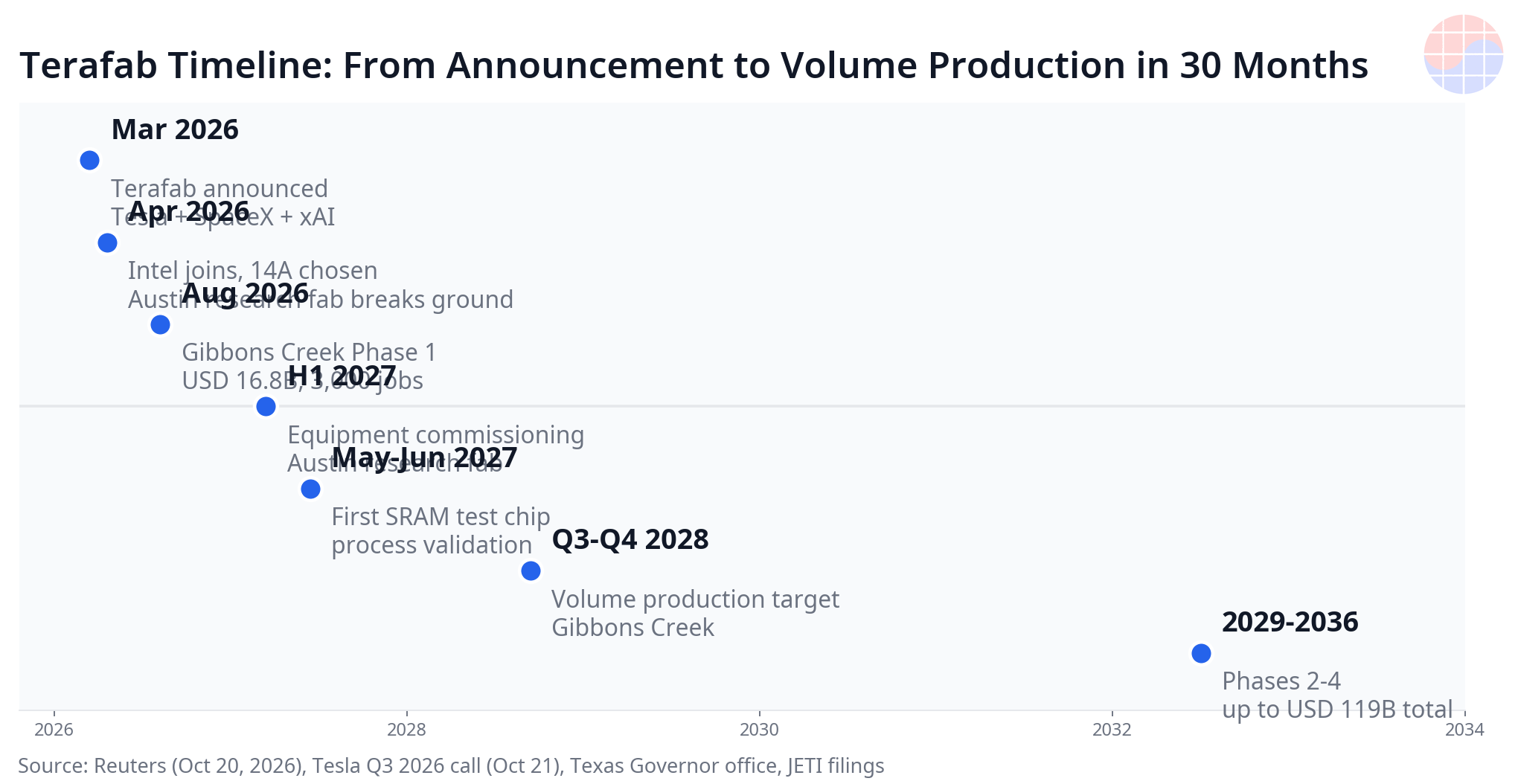
On the SpaceX Q3 earnings call on October 20, 2026, Elon Musk turned Terafab's internal targets into a concrete calendar for the first time. Asked by Morgan Stanley's Adam Jonas, he said the first test chip would run at the Austin research facility around May-June 2027, and that main fab volume production in Q3 2028, or Q4 at the latest, was "within the set of possible outcomes." The next day, on the Tesla Q3 call on October 21, CFO Vaibhav Taneja confirmed that most of the first equipment orders for the research fab were complete, and Musk said tens of billions of dollars would go into equipment alone by early 2028, with the long-term total exceeding $100 billion. How Tesla and SpaceX split the cost has not been decided.
| Date | Milestone | Location | Notes |
|---|---|---|---|
| March 21, 2026 | Terafab officially announced | Austin | Joint Tesla, SpaceX, and xAI project |
| April 7, 2026 | Intel joins the project | - | Design, manufacturing, and packaging collaboration |
| April 2026 | Research fab construction begins | North campus of Giga Texas | About $3 billion invested, a few thousand wafers per month |
| August 6, 2026 | Main fab site confirmed, Phase 1 at $16.8 billion | Grimes County, Gibbons Creek | 3,000 jobs, $30 million Texas state grant |
| December 1, 2026 | Main fab construction scheduled to start | Grimes County | Per Texas state filings, completion target end of 2028 |
| First half of 2027 | Research fab equipment commissioning begins | Austin | Confirmed on Tesla call |
| May-June 2027 | First SRAM test chip target | Austin | Process validation vehicle, not a commercial chip |
| Q3-Q4 2028 | Volume production start target | Gibbons Creek | Musk noted a large error bar |
| 2029-2036 | Phase 2-4 expansion | Grimes County | Per JETI filings, cumulative maximum of $119 billion |
The comparison shows how aggressive this schedule is. In the United States, an advanced logic fab typically takes more than three years from groundbreaking to volume production. Samsung's Taylor fab and TSMC's Arizona fab both took longer than that from announcement to production, and those are companies that have run fabs for decades. Terafab is a plan by a company with no fab operating experience to bring in a process that is not yet complete (Intel 14A) and reach volume production 30 months after announcement. So the essence of this schedule is not a construction schedule but a learning schedule. The dates will be set not by how fast buildings go up, but by how fast the process is learned.
Why the First Chip Is SRAM: Standard Process Development, and an Honest Signal
The fact that the first test chip is SRAM, not an AI accelerator, is the most honest part of this project. SRAM is the standard test vehicle for process development. A bitcell made of six transistors repeats in a dense array, so a single wafer can quantify defect density, leakage current, minimum operating voltage (Vmin), and bitcell yield. SRAM fails before logic standard cells do, which makes SRAM yield the health certificate of a process.
On timing, SRAM is also the first circuit to fail. Bitcell read stability and write margin are the most sensitive to process variation, and sense amplifier offset exposes device mismatch directly. So SRAM chips merely "working" in May-June 2027 is not enough. Three numbers matter. First, whether wafer defect density sits on the learning curve. Second, whether the SRAM Vmin distribution converges below the target voltage. Third, whether the result repeats across multiple lots, not just one wafer. Only when all three are confirmed can the 2028 production target be read as a process schedule. Conversely, if the SRAM schedule slips, every date behind it slips automatically. SRAM is this project's first moment of truth.
The research fab's design concept matches this. Tesla says the core of the research fab is a closed loop in one building: make the mask, print the chip, test it, and fix the mask. In the current industry, wafers travel between the design company, the fab, and the packaging house, and each cycle takes weeks. The Terafab research fab aims to finish that iteration cycle inside one building. Tesla claims no fab in the world has an integrated test facility like this. It is not a production fab but a factory that sells learning speed. That is what the research fab is.
Fab Feature 1: Two Fabs, Two Missions
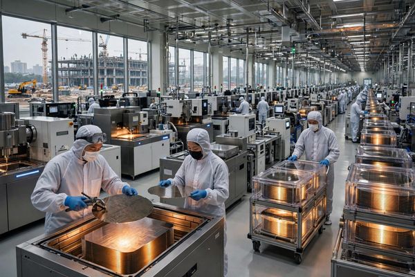
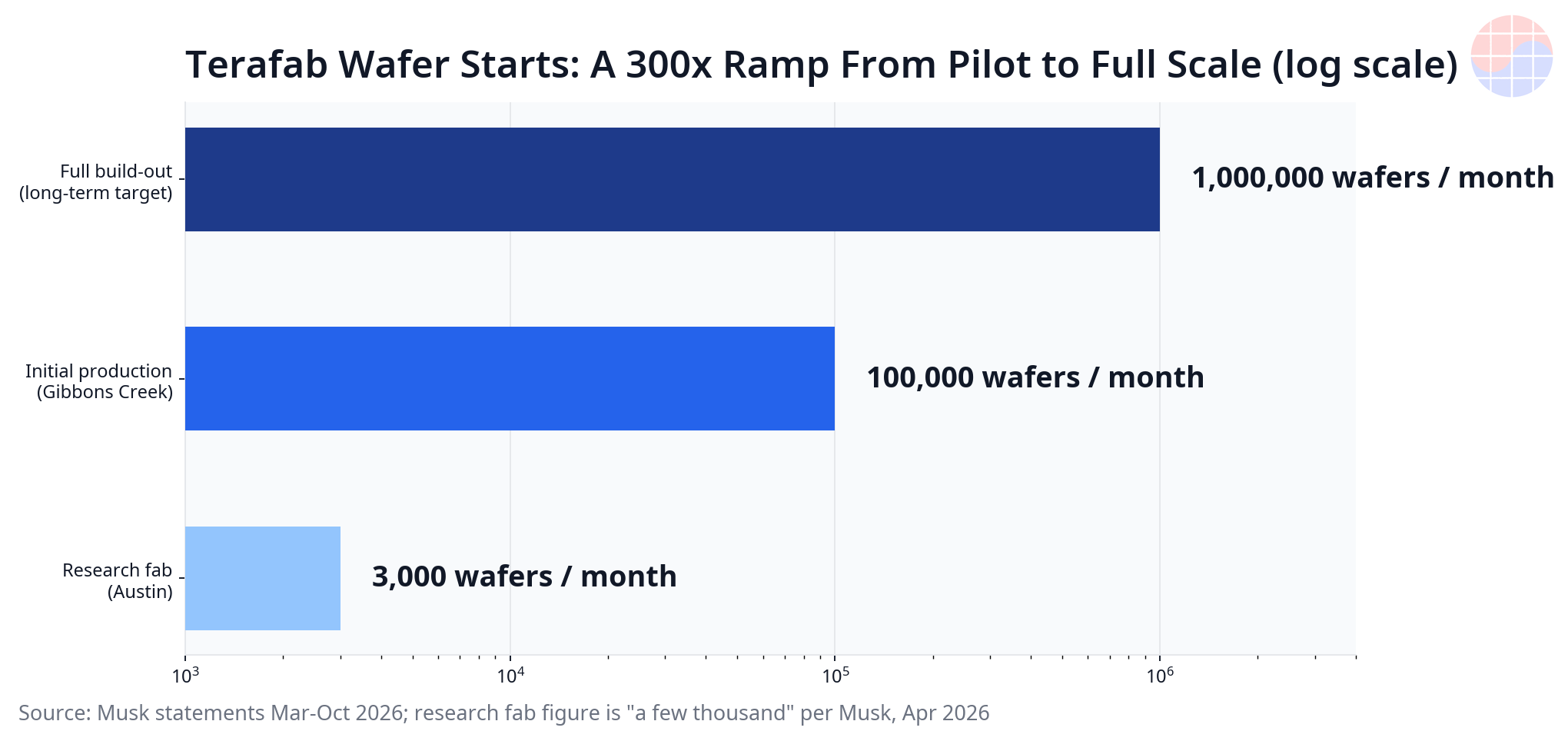
Terafab is not one factory but two fabs with completely different roles. The Austin research fab is a small pilot line on the north campus of Giga Texas, at a scale of a few thousand wafers per month, with the mission of rapidly testing process recipes, transistor structures, and packaging variants. The Grimes County main fab is the volume production fab on the former Gibbons Creek power plant site, about 145 km northwest of Houston, targeting 100,000 wafers per month initially and 1 million per month long term. Only what is validated at the research fab moves to the main fab. This separation is industry common sense. An experimental line's time cannot be shared with a production line, and a production line cannot accept experimental recipe changes.
Fab Feature 2: Logic, Memory, and Packaging Under One Roof
This is why Musk calls Terafab "the most epic chip manufacturing attempt." In a normal semiconductor supply chain, TSMC or Samsung handles logic, SK hynix and Micron handle memory, and yet another company handles packaging. Terafab plans to put every step, from mask design to logic manufacturing, memory manufacturing, advanced packaging, and test, on one campus. The site covers more than 6,000 acres, with a final planned floor area of 100 million square feet. At roughly 4 km in length, it is one of the largest single manufacturing facilities in the world.
The hardest cell in this integration is memory. Logic and DRAM processes are entirely different specialties, in equipment configuration, cell structure, and yield learning method. John Lawlor of French market research firm Yole pointed out that memory manufacturing is a separate specialty that none of Tesla, SpaceX, or Intel possesses. Reports say Terafab is hiring memory process engineers, but between a job posting and production capability lie years of learning. Producing even HBM in-house is the least validated part of this project. Integrating logic and packaging is aggressive but within the range of the imaginable. Internalizing memory is one step further away.
Fab Feature 3: A Fab With No Customers, Where Demand Is the Owner
Terafab is not a foundry. It does not sell capacity to external customers. All output goes into Tesla vehicles and Cybercab, Optimus robots, SpaceX Starlink satellites and space data centers, and xAI compute demand, making it a captive fab. Musk's logic is simple. Even if you add up the output of every fab in the world, it is only about 2% of what his companies will need. Hence the line: "build Terafab, or have no chips."
📩 Following this story?
Get the follow-up analysis — earnings, reports and HBM supply — in your inbox daily at 10:30 KST. Subscribe free →
The long-term target of 1 terawatt (TW) of compute must be read in this context. The goal is to make the combined compute of chips produced per year reach the 1 TW class. Unpacking the number shows its weight. By industry media conversions, it corresponds to wafer volumes equivalent to about 22.4 million NVIDIA Rubin Ultra-class GPUs and about 15.8 million HBM units, requiring well over 100 fabs of the current kind. In other words, 1 TW is not a 2028 production plan. It is a distant target that remains far away even after all four expansion phases finish and the 1 million wafers per month system is complete. This number must not be read as near-term capacity.
Fab Feature 4: The Process Is Intel 14A, and the Operator Debate Is Ongoing
The process substance of Terafab is not in-house development but Intel 14A (1.4 nm class). Musk confirmed the use of 14A directly on the Tesla call in April 2026, saying it is "not yet a fully complete process, but by the time Terafab scales up it should be mature enough." For Intel, this secures the "meaningful external customer" that was a condition for 14A's survival. For Terafab, the project's technology clock is now tied to Intel's clock. If 14A risk production and volume schedules slip, Terafab's 2028 target slips with them. Intel packaging technologies such as Foveros 3D stacking and EMIB are also part of the structure, so the dependence spans the entire manufacturing stack, not just one process step.
The tug-of-war over who operates the fab is not over either. In early October, Musk acknowledged there had been talks with TSMC, but then drew a line: "we build the fab and we operate it; TSMC can lease part of the site at most, if it wants." In contrast, TSMC Chairman C.C. Wei stated on the October 15 earnings call the principle that if TSMC cooperates, TSMC must operate the fab. The two statements cannot both hold. The accurate reading today is that Intel is the only confirmed manufacturing partner, and TSMC has only a leasing possibility open.
Fab Feature 5: A Fab Not Connected to the Power Grid
The Terafab main fab is designed not to buy electricity from the power grid. According to tax agreement documents with Grimes County, the campus will source power from its own natural gas power plant and large-scale battery storage, and is specified not to use grid electricity. Water will come not from groundwater but from the Gibbons Creek reservoir, with a closed-loop recycling system and its own wastewater treatment facility. This is why the former coal power plant site was chosen. The reservoir and land the power plant used convert directly into the semiconductor campus's utilities.
This choice directly bypasses the point that power procurement and permitting are the biggest bottlenecks in US fab construction. In exchange, it takes on new bottlenecks: gas turbine procurement and power generation permits. Either way, hidden in Terafab's schedule, alongside semiconductor equipment, are the delivery dates of power equipment.
Fab Feature 6: Terrestrial Chips and Space Chips Under One Roof
Production items split into two lines. One is terrestrial inference chips for vehicles and robots, centered on Tesla's AI5 and AI6 families. AI5 is currently being made on Samsung's 2 nm process at the Taylor fab, and Terafab is designed as the in-house base for the successor generations. The other is chips for orbital data centers. In the space environment, radiation and heat dissipation conditions differ completely from the ground, so the chip design itself must change. The AI satellite design SpaceX disclosed in June 2026 is the substance of this demand. Printing two product families with nearly opposite requirements, terrestrial inference and space compute, on one campus is also a configuration no existing fab has.
Fab Feature 7: Building the Supply Chain From a Blank Page, With Korean Companies on the First Page
Building a fab from a blank page means building the supply chain from a blank page too. That movement was spotted at SEMICON West in San Francisco on October 13-15, 2026. Tesla and SpaceX staff visited the booths of about 10 Korean companies directly, and more than half signed non-disclosure agreements. Progress confirmed so far differs by company, so it must be read by stage.
| Company | Item Under Discussion | Confirmed Stage |
|---|---|---|
| HPSP | High-pressure hydrogen annealing equipment | Agreement to supply 1 unit for the research line, the only confirmed equipment deal |
| Hanmi Semiconductor | Packaging equipment including TC bonders | Supply discussions and order reports stage |
| Komico (Mico group) | Cleaning services | Three-way NDA with Tesla and SpaceX |
| Unisem | Environmental equipment including scrubbers | NDA signed |
| Dongjin Semichem | Process materials including thinner and phosphoric acid | Discussions linked to its Texas plant for 2-3 months |
| ISC | Test sockets | Samples and design information exchanged |
| ENF Technology, Asflow, BMT, GnG Intech | Process materials, piping and valves, wastewater recycling | Initial contact and product review |
So far there is only one confirmed contract, HPSP, and it is for the research line, not the production fab. The rest are pre-contract stages. What matters is that the contact range spans nearly the entire fab, from equipment to materials, piping components, and wastewater recycling. It is a signal that Terafab views the Korean supply chain not as a backup line but as a candidate for the main supply chain. Whether equipment main contracts grow from research line to production line scale will be the fastest gauge of this project's execution stage.
The Bottleneck Is Equipment: No Answer to the EUV Question
The most meaningful silence on the October 20 call came on the EUV question. Asked whether ASML extreme ultraviolet lithography equipment had been ordered, Musk did not answer directly, instead thanking ASML and its partners for pulling in delivery dates. ASML has said its orders are booked through 2028, and KLA has said lead times for some products have stretched from the usual 12 months to 18-24 months. ASML and Applied Materials shares rising about 3% after hours right after Musk's remarks shows how the market reads this bottleneck. For equipment makers, a new fab customer means more orders. For every US fab, including Samsung Taylor and TSMC Arizona, it means deeper competition in the equipment queue. The more Terafab pulls its delivery dates forward, the further back someone else's dates move.
Impact on Korea: No Immediate Order Shift, and Competition Starts in Texas
Starting with the short-term impact, Samsung's Tesla volumes stay as they are. The contracts for AI5 and AI6 produced on Samsung Taylor 2 nm are alive, and until the second half of 2028, Terafab's production target, every advanced chip Tesla uses comes from the existing supply chain. Terafab does not take Samsung orders away immediately.
Mid-term competition comes on three levels. First, workforce competition in the same Texas neighborhood. The Terafab site is not far from Samsung Taylor, and the pool of skilled process engineers is limited. Reports that Samsung dispatched yield engineers from headquarters to Taylor, and Terafab's memory engineer hiring, point at the same labor market. Second, equipment procurement competition. Third, at the furthest level, demand internalization. If Terafab actually produces volume after 2029, the incremental demand of a large customer, Tesla, leaves the foundry market. Conversely, if Terafab fails at memory internalization, HBM and DRAM demand stays with SK hynix and Samsung. For Korean companies, the worst scenario is not Terafab succeeding. It is Terafab absorbing equipment and engineers while failing at production, raising fab ecosystem costs across Texas.
Dates to Watch
- December 2026: Whether Grimes County main fab construction starts on the December 1 schedule in the filings
- First half of 2027: Austin research fab equipment move-in and commissioning start, checkable repeatedly on Tesla quarterly calls
- May-June 2027: Whether the SRAM test chip announcement comes with quantitative yield figures. A success declaration without numbers is half a signal
- During 2027: Whether the Intel 14A risk production schedule holds. Terafab's clock is tied to this clock
- 2027-2028: Whether Korean suppliers' research line contracts grow into production line main contracts, and whether EUV orders are officially confirmed
- Q3 2028: The form of the production declaration. Small shipments and high-yield volume production are different sentences
Conclusion: Terafab Is Not a Construction Story but a Learning Speed Experiment
Seen as a building, Terafab leaves only the numbers: the world's largest floor area and $119 billion. Seen as a process, the picture differs. This project's outcome depends on whether three learning curves converge inside the date called 2028: the maturity curve of the Intel 14A process, the yield learning curve of a team with no fab operating experience, and the integration curve of putting logic and memory under one roof. If just one of the three is late, the production date moves.
So the way to read it changes too. Groundbreaking photos and investment amounts are not progress. Progress is confirmed only in the 2027 SRAM yield numbers, the scale of equipment main contracts, and the 14A schedule. What Musk's companies showed with electric vehicles and rockets is a record of eventually delivering part of an impossible-looking schedule, and at the same time a record of that schedule slipping by years. Terafab's 2028 is the date where those two records collide head-on. The first verdict comes in May-June 2027, in Austin.
Frequently Asked Questions
When does Terafab make chips?
On internal targets, the first SRAM test chip at the Austin research fab in May-June 2027, and volume production starting at the Grimes County main fab in Q3-Q4 2028. It is a target schedule for which Musk himself noted a large error bar. (Earnings calls, October 20-21, 2026)
What chips does Terafab make?
The targets are AI inference chips for Tesla vehicles and the Optimus robot (successors to the AI5 and AI6 families) and chips for SpaceX orbital data centers. The structure is designed to perform logic, memory, advanced packaging, and test on one campus.
What process node does Terafab use?
It will use Intel 14A (1.4 nm class). Intel cooperates on design, manufacturing, and packaging, and 14A itself has not yet reached production maturity, so there is schedule linkage risk.
How large is the Terafab investment?
Phase 1 at $16.8 billion has been officially confirmed, and Texas state filings show a cumulative maximum of $119 billion across four phases. Musk said tens of billions of dollars go into equipment alone by early 2028, with a long-term total above $100 billion. (Tesla call, October 21, 2026)
What is the impact on Samsung and SK hynix?
In the short term, Samsung's Tesla AI5 and AI6 volumes are maintained. In the mid term, competition intensifies for engineers in Texas and for semiconductor equipment procurement. About 10 Korean equipment and materials companies have already signed NDAs with Terafab or are discussing supply, and HPSP has agreed to supply research line equipment.
📩 Missed today's analysis? Get tomorrow's in your inbox
Daily Silicon at 10:30 KST plus earnings and analyst-report breakdowns, first. Samsung Electronics, SK hynix, TSMC and HBM supply, read by practicing engineers. Join 300+ subscribers.
Subscribe free →
Free · No spam · Unsubscribe anytime