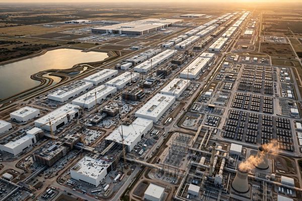
VLSI Korea
YMTC Production Is Now Huge: 500K Wafers a Month Target, No. 3 in NAND Shipments
YMTC NAND output is surging. Shipment share hit 16.5% in Q2 2026 for No. 3 globally, and 2027 wafer output grows by 486K wafers, 6.5 times the Samsung and SK hynix increase. What the 500K a month target means, in numbers.


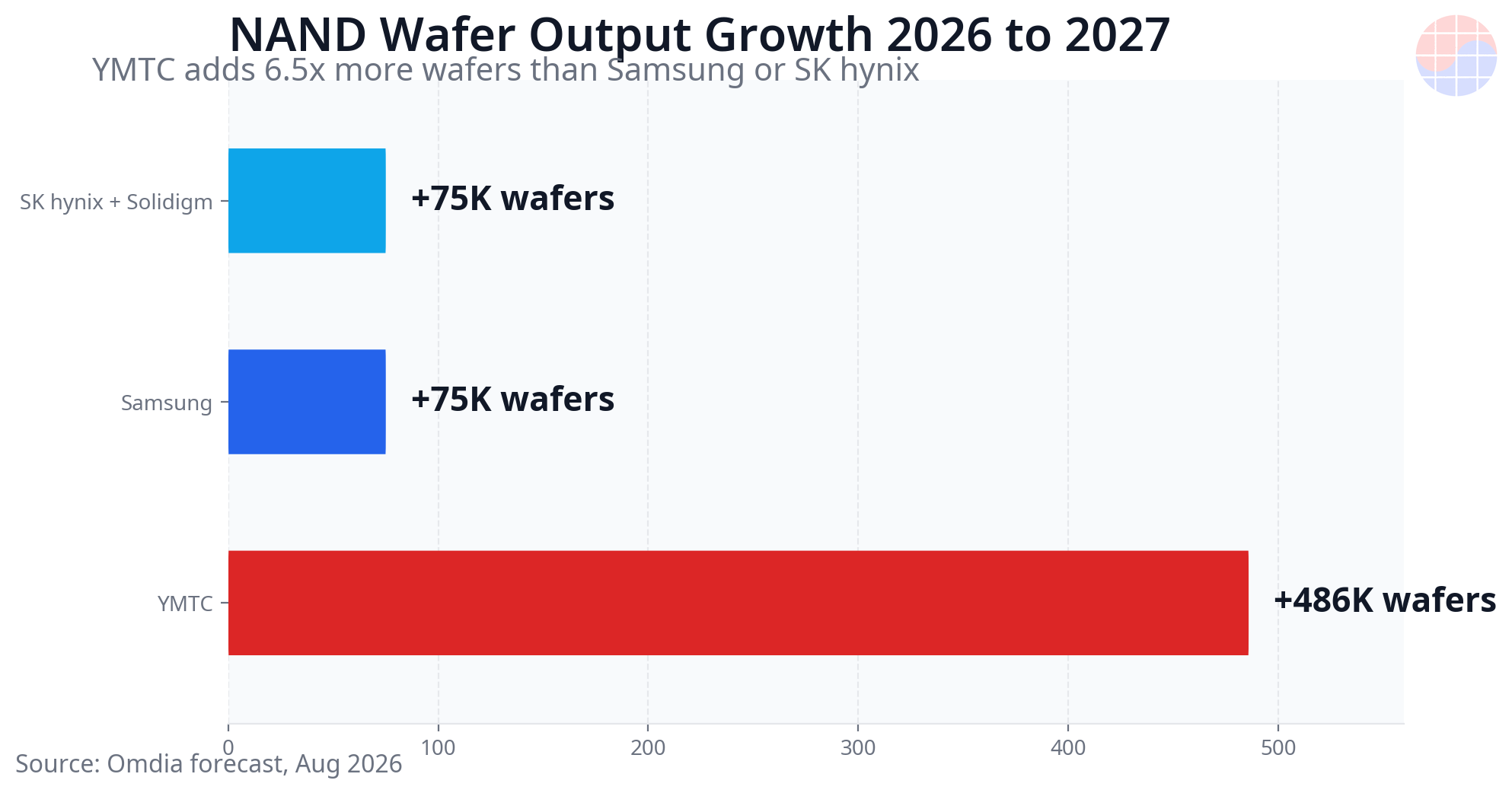
YMTC's NAND production volume is now too large for Samsung and SK hynix to treat as a side story. Counterpoint Research data published on October 22, 2026 puts YMTC's global NAND shipment share at 16.5% in Q2 2026, ranked No. 3 worldwide. Omdia forecasts YMTC's annual wafer output rising from 2.01 million wafers in 2026 to 2.496 million in 2027, an increase of 486,000 wafers. Samsung and SK hynix each add only 75,000 wafers over the same period. YMTC alone adds 6.5 times more wafers than either Korean rival.
The target is larger still. YMTC has set a long-term NAND shipment share goal of 20% and is pushing total wafer capacity, including DRAM, toward about 500,000 wafers per month. That would exceed Samsung's estimated NAND capacity of 390,000 to 450,000 wafers per month. On physical wafer volume alone, the world's largest NAND producer could change.
Key numbers
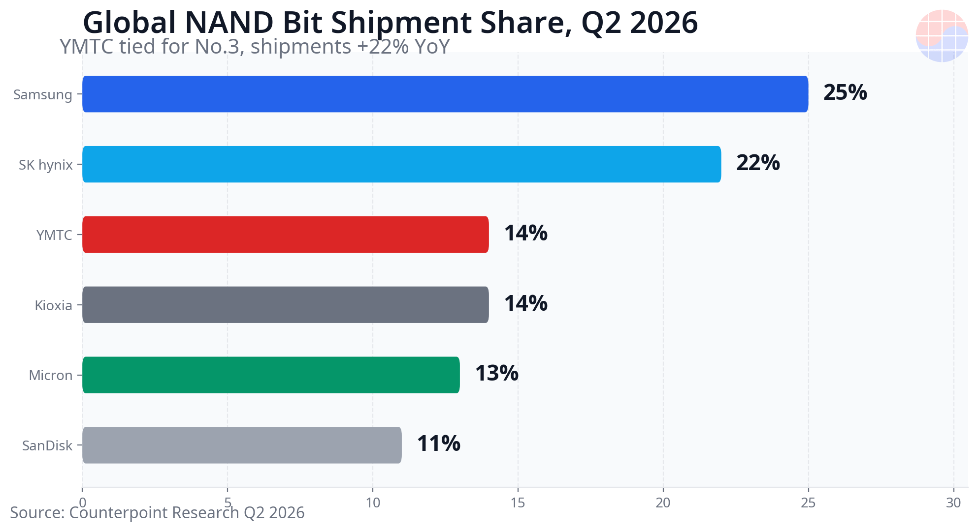
- Shipment share: 16.5% in Q2 2026, No. 3 globally (Counterpoint, October 22, 2026). By bit shipments the share is 14%, tied for No. 3 behind Samsung at 25% and SK hynix at 22%, with bit shipments up 22% year over year.
- Output growth: Plus 486,000 wafers in 2027, up 24.2% (Omdia), versus plus 75,000 wafers for Samsung and plus 75,000 for SK hynix including Solidigm.
- Wuhan Fab 3: Output jumps more than sixfold, from 90,000 wafers in 2026 to 575,000 in 2027. Most of the total increase comes from this single fab.
- China share: YMTC leads in China at 38.5%, ahead of Samsung at 33.5% and SK hynix at 17%. A year earlier YMTC held 28% in China.
- Capacity path: About 200,000 wafers per month today, about 300,000 with Fab 3, about 400,000 with Fabs 4 and 5, and a final target near 500,000 including DRAM.
- R and D: 14.2 billion yuan invested from 2023 to 2025, 4,796 R and D staff at over 30% of all employees, and 5,611 registered invention patents.
1. Production: the growth rate is the story
The core fact is not absolute size but growth speed. Samsung and SK hynix are reallocating capacity toward DRAM and HBM. Samsung's Pyeongtaek P5 NAND output ramps only from 2027 to 2030, and SK hynix's Cheongju M17 first cleanroom is scheduled for December 2028. For both Korean makers, meaningful NAND volume growth is effectively a post-2028 story.
YMTC is running the other way. Wuhan Fab 1 runs at about 100,000 wafers per month and Fab 2 at about 60,000, both close to full utilization. Fab 3 starts initial operations at the end of this year and enters full mass production next year, which is where the step change comes from.
| Company | 2026 forecast | 2027 forecast | Increase |
|---|---|---|---|
| YMTC | 2.01M wafers | 2.496M wafers | +486K (+24.2%) |
| Samsung | 4.77M wafers | 4.845M wafers | +75K |
| SK hynix incl. Solidigm | 2.79M wafers | 2.865M wafers | +75K |
Source: Omdia forecast as reported in August 2026. In plain terms, most of the new NAND wafers entering the market in 2027 will come from Wuhan.
2. Share: No. 3 globally, already No. 1 in China
The share number depends on the yardstick. Counterpoint's shipment-based figure, drawn from YMTC's Shanghai STAR Market listing application and published on October 22, is 16.5%. Its memory tracker bit-shipment figure is 14%, tied with Kioxia for No. 3. Both point the same way: YMTC has passed Kioxia and Micron on shipments, and only Samsung and SK hynix remain ahead.
Inside China the order has already flipped. YMTC holds 38.5% of China's NAND market, ahead of Samsung at 33.5% and SK hynix at 17%. That shift is what pushed Samsung to upgrade its Xian fab from about 200 layers to 286-layer V9, with reported plans for 5,000 wafers by the end of 2026 and 40,000 by the end of 2027, and SK hynix to upgrade its Dalian fab as well.
3. The capacity roadmap: what 500,000 wafers a month means
YMTC's current capacity across its two Wuhan fabs is estimated at about 200,000 wafers per month. Fab 3 takes that to about 300,000, two additional fabs to about 400,000, and the company-wide target including DRAM is about 500,000 wafers per month.
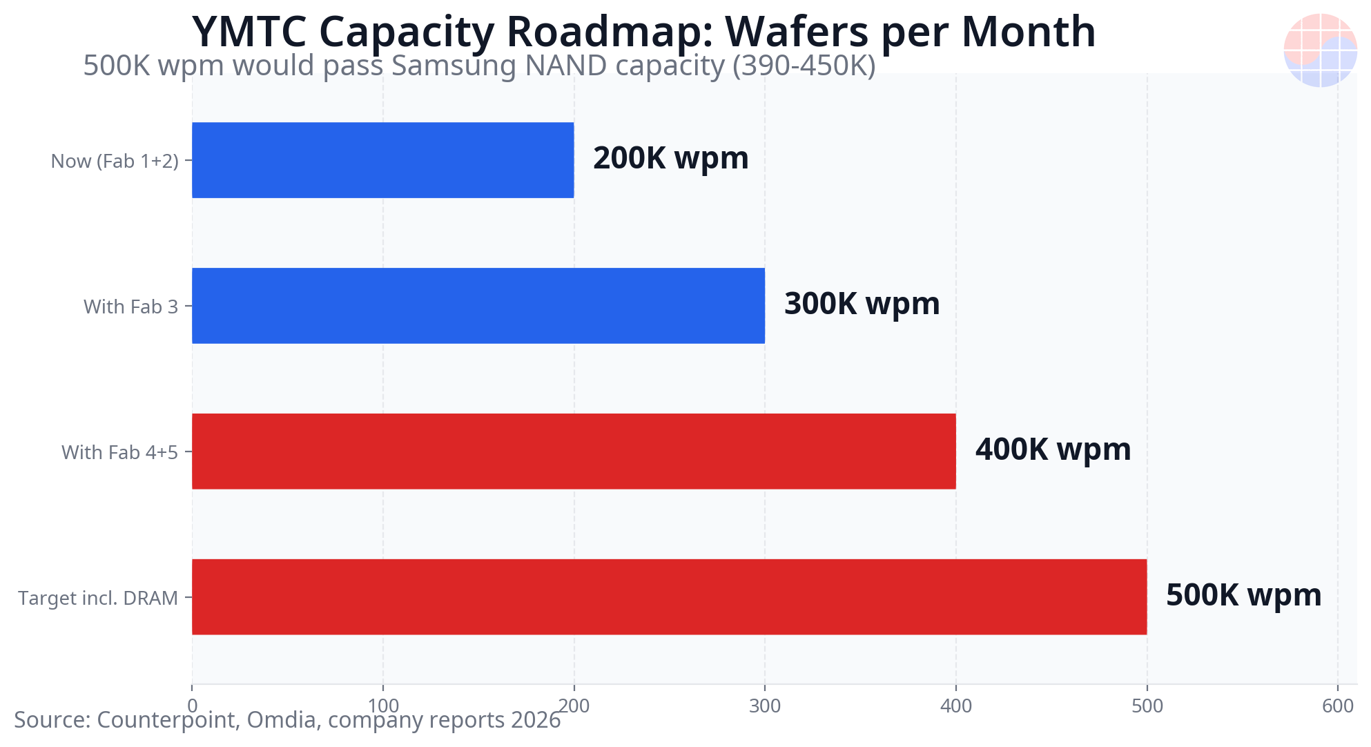
The comparison is why the target matters. Samsung's NAND capacity is estimated at 390,000 to 450,000 wafers per month. Reaching its target would make YMTC the largest NAND producer by wafer starts. Wafer starts are not bit output, however. Layer count, yield and product mix decide bit cost, and volume leadership is not revenue leadership, which is the subject of the next sections.
4. How it is possible: Xtacking and domestic tools
The foundation is Xtacking, YMTC's bonding architecture. The memory cell array and the peripheral circuits are built on separate wafers and then bonded together. Each side can use the process that suits it, and layer counts can keep rising on mature deep-ultraviolet tools without extreme-ultraviolet lithography. Under export controls that block EUV access, that structure doubles as a survival strategy.
YMTC is mass-producing 267-layer 3D NAND on Xtacking 4.0 and has shipped a 294-layer part built by bonding two decks. A 300-plus-layer generation is planned for next year. Samsung's own behavior underlines the technology's weight: in February 2025 Samsung licensed YMTC's Xtacking-related patents. Industry counts also put YMTC's hybrid bonding core patents at 119, ahead of Samsung at 83 and SK hynix at 11.
Domestic tooling is the other engine. Wuhan Fab 3 has been reported as the first major Chinese memory fab where domestic equipment exceeds 50% of the tool set, with Chinese vendors gaining share quickly in etch, deposition, cleaning and metrology. Lithography remains the weak link, but every other step that gets localized helps YMTC keep building fabs at speed under sanctions.
5. No. 3 on volume, No. 5 on revenue: the wall not yet crossed
YMTC's weakness is visible in its own numbers. It ranks third in bit shipments but only fifth in revenue, behind Kioxia and Micron. The reason is product mix. Its output is still weighted toward consumer products, while the money sits in enterprise SSDs, which took 48% of all NAND bits in Q2 2026 and are expected to pass 50% by year end.
📩 Following this story?
Get the follow-up analysis — earnings, reports and HBM supply — in your inbox daily at 10:30 KST. Subscribe free →
Price is a double-edged weapon. YMTC products are assessed at 10 to 20% cheaper than Korean and Japanese rivals. That buys share, but converting volume into revenue and profit requires enterprise SSD qualification and data center customers. Counterpoint views 15% share as the minimum at which a NAND maker can self-fund future capital spending. YMTC has reached that line. The next test is mix, not volume.
6. After NAND comes DRAM
YMTC is extending its bonding technology into DRAM. Since October 2025 it has been developing and testing 16Gb LPDDR5 at Fab 2 at a scale of about 5,000 wafers per month, at 7500MT/s and without high-k metal gate so far. The follow-on product applies a vertical channel transistor and a 4F2 cell structure for 9600MT/s LPDDR5, planned for mass production at Fab 3.
Counterpoint research vice president Neil Shah argues that 3D DRAM is ultimately where the industry must go, and that YMTC, with proven stacked wafer bonding, is well positioned for that transition. DRAM qualification barriers are higher than NAND's, however, and yield plus customer qualification will decide whether this becomes a business. Today it is a pilot, not a confirmed mass production schedule.
7. What it means for Korean makers
First, NAND prices. TrendForce expects NAND supply to loosen and downward price pressure to build from the second half of 2027 as new capacity lands, and YMTC sits at the center of that new capacity. If Chinese volume arrives while consumer demand is weak, price declines can accelerate.
Second, China fab strategy. Both Korean makers are answering share losses in China with node upgrades in Xian and Dalian. See the earlier analysis of Samsung and SK hynix China NAND fab upgrades and the six-company comparison in Memory Giants Compared.
Third, the opportunity cost of the HBM pivot. The Korean NAND plateau is a choice: limited capital went to HBM and DRAM, and YMTC filled the space left behind. How long a technology lead can offset a volume deficit is now the open question in NAND.
8. Risks: sanctions remain the largest variable
YMTC has been on the US Commerce Department Entity List since December 2022. Advanced tool procurement is blocked and overseas customer qualification is constrained, which is why so much of its volume is absorbed inside China. Additional US legislation under discussion targets even the deep-ultraviolet lithography, etch and deposition tools that the Xtacking roadmap relies on, so its outcome can set the speed of that roadmap.
Other risks remain open: domestic tool yields, the bit cost of the 300-plus-layer transition, enterprise SSD qualification speed, and whether the financial disclosure that comes with a public listing supports the growth story told so far. The production expansion itself is a confirmed fact. Whether it converts into profit is not yet proven.
Frequently asked questions
Q. What exactly is YMTC's NAND market share?
A. It depends on the basis. On shipments, Counterpoint put YMTC at 16.5% in Q2 2026 in data published on October 22, 2026. On bit shipments it is 14%, tied for No. 3 behind Samsung at 25% and SK hynix at 22%. YMTC's long-term target is 20%.
Q. How much will YMTC production grow?
A. Omdia forecasts annual wafer output rising from 2.01 million wafers in 2026 to 2.496 million in 2027, up 486,000 wafers or 24.2%. Wuhan Fab 3 output rising from 90,000 to 575,000 wafers, more than sixfold, accounts for most of the increase.
Q. Will YMTC make more NAND than Samsung?
A. On wafer capacity targets, it could. YMTC's target including DRAM is about 500,000 wafers per month, above Samsung's estimated NAND capacity of 390,000 to 450,000. Bit output and revenue still depend on layer count, yield and mix, and YMTC remains No. 5 on revenue.
Q. How does YMTC expand while under US sanctions?
A. Two factors matter most. The Xtacking structure raises layer counts on existing tools without EUV, and domestic equipment now exceeds 50% of the tool set at Fab 3 across steps such as etch and deposition. Lithography remains a constraint.
Q. Does YMTC make DRAM?
A. It is at the development and pilot stage. It is testing 16Gb LPDDR5 at about 5,000 wafers per month at Fab 2 at 7500MT/s, with a 9600MT/s next generation planned for Fab 3. Qualification and mass production timing are not yet confirmed.
Sources: Counterpoint Research memory tracker and October 22, 2026 listing-related analysis, Omdia NAND wafer output forecast as reported in August 2026, Reuters reporting on Samsung's Xian fab upgrade. Capacity figures are agency estimates and reporting, not company disclosures, and the basis (shipments, bits, wafers) is stated in the text. As of October 23, 2026.
📩 Missed today's analysis? Get tomorrow's in your inbox
Daily Silicon at 10:30 KST plus earnings and analyst-report breakdowns, first. Samsung Electronics, SK hynix, TSMC and HBM supply, read by practicing engineers. Join 300+ subscribers.
Subscribe free →
Free · No spam · Unsubscribe anytime