VLSI Korea
Samsung and SK hynix Upgrade China NAND Fabs: 5 Facts Behind the 286-Layer and 240-Layer Moves (V9, YMTC)
Samsung's Xi'an fab converts from about 200 layers to 286-layer V9 NAND and SK hynix's Dalian fab moves from 192 to 240 layers and above. Five facts on YMTC's 38.5% China share, the US licence line, and the ramp, from Reuters reporting on Oct 21, 2026.


Samsung and SK hynix Upgrade China NAND Fabs: 5 Facts Behind the 286-Layer and 240-Layer Moves (V9, YMTC)
Samsung Electronics and SK hynix are converting their China NAND fabs to 286-layer and 240-layer-class production — not expanding capacity, but closing a one-generation technology gap before YMTC closes it for them.
TL;DR
- Samsung Electronics and SK hynix are upgrading their China factories to produce more advanced NAND flash, to fend off competition from YMTC and to meet AI-driven demand (Reuters reporting, Oct 21, 2026).
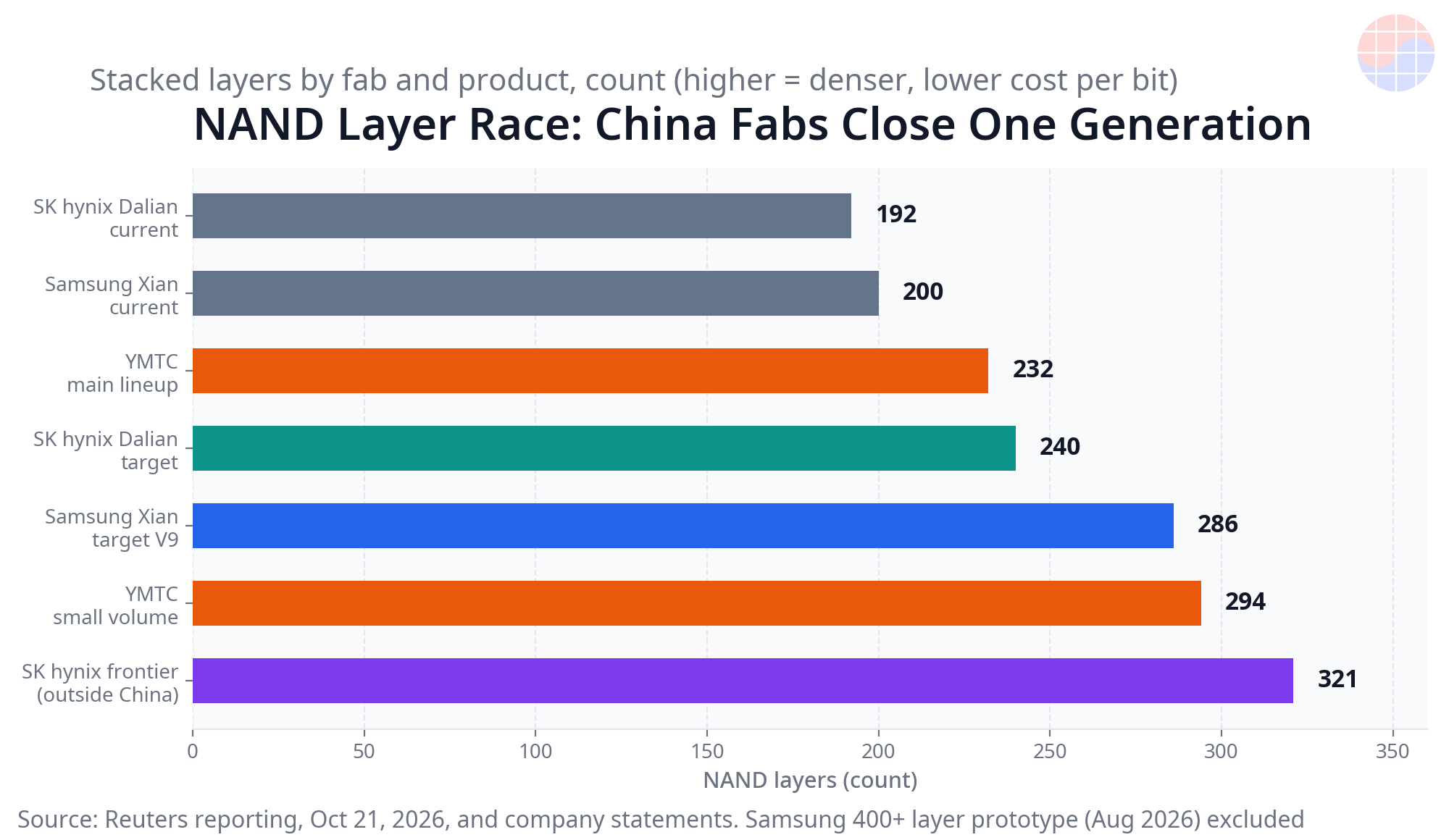
- Samsung's Xi'an fab, about 40% of Samsung's global NAND output, runs at about 200 layers today and is being converted to 286-layer V9 NAND under an internal project, with a target of 5,000 wafers per month in December 2026 and 40,000 wafers per month by December 2027 (Reuters reporting, Oct 21, 2026).
- SK hynix's Dalian fab runs at 192 layers today and is switching to 240 layers and above (Reuters reporting, Oct 21, 2026).
- In China's NAND market, YMTC reached a 38.5% share in Q2 2026, ahead of Samsung at 33.5% and SK hynix at 17% (industry data cited by Reuters, Oct 21, 2026).
- Both companies told Reuters the upgrades are underway in close consultation with Washington, and Samsung stated the Xi'an upgrade complies with US export regulations, meets growing global customer demand including in the US, and does not expand capacity or build new facilities (company statements to Reuters, Oct 21, 2026).
5 Facts
- The upgrades are conversions, not new fabs. Samsung Electronics and SK hynix are upgrading existing China factories to produce more advanced NAND, and Samsung stated explicitly that the Xi'an work is not a capacity expansion and involves no new facilities (company statement to Reuters, Oct 21, 2026; Reuters reporting, Oct 21, 2026).
- Samsung Xi'an jumps about 43% in layers, from about 200 to 286. The internal conversion project targets 286-layer V9 NAND, starting at 5,000 wafers per month in December 2026 and reaching 40,000 wafers per month by December 2027, an eightfold ramp in 12 months (Reuters reporting, Oct 21, 2026; layer increase and ramp multiple are VLSI Korea calculations).
- SK hynix Dalian moves from 192 layers to 240 layers and above, a 25% step. The Dalian fab, acquired in 2021 through the purchase of Intel's NAND business, is the sole NAND fab of Solidigm, the US subsidiary preparing a US IPO, and one source said authorisation extends up to 240 layers, with possible permission sought for research on 300 layers and above (Reuters reporting, Oct 21, 2026; percentage is a VLSI Korea calculation).
- YMTC has already taken the lead in its home market. YMTC's share of China's NAND market rose from 28% in 2025 to 38.5% in Q2 2026, while Samsung moved from 36% to 33.5% and SK hynix from 20% to 17% — a 13-percentage-point swing between YMTC and Samsung (industry data cited by Reuters, Oct 21, 2026; swing is a VLSI Korea calculation).
- The upgrades close the China-fab gap to the current commercial frontier, not beyond it. Outside China, Samsung already sells NAND up to 286 layers and SK hynix up to 321 layers, while YMTC's lineup is mostly 160-layer and 232-layer products with a small amount of 294-layer output — so a 286-layer Xi'an does not leapfrog YMTC's best silicon, it removes the China fabs' one-generation handicap (Reuters reporting, Oct 21, 2026).
Background
NAND flash retains data without power. It sits inside smartphones, PCs, and the SSDs that feed AI data centres. The basic economics are set by stacking: the more word-line layers a NAND die carries, the more bits fit on the same silicon area, and the lower the cost per bit falls. Layer count is therefore not a vanity metric. It is the cost curve itself (technology background, as of Oct 21, 2026).
That is why the starting positions matter. Samsung's Xi'an fab produces about 40% of Samsung's global NAND output, yet it has been running at about 200 layers while Samsung sells up to 286-layer NAND produced outside China. SK hynix's Dalian fab has been running at 192 layers while SK hynix sells up to 321-layer NAND elsewhere. In both cases the China fab trails the company's own commercial frontier by roughly one generation (Reuters reporting, Oct 21, 2026).
The reason for the lag is regulatory, not technical. Since 2022, US export controls have required Samsung and SK hynix to obtain annual US licences to install US-made equipment, such as etching tools, in their China factories. In 2025, the US Bureau of Industry and Security said it did not intend to grant licences to upgrade technology or expand capacity at foreign makers' China factories, and it told Reuters it intends to grant licences to operate existing factories, not to expand capacity or upgrade technology (Reuters reporting, Oct 21, 2026). Any upgrade therefore has to be framed, engineered, and licensed as something other than an expansion — which is exactly how both companies are describing it.
Meanwhile the competitive clock is running. YMTC's share of the China NAND market rose from 28% in 2025 to 38.5% in Q2 2026 (industry data cited by Reuters, Oct 21, 2026). AI demand is simultaneously pulling high-density NAND into data-centre SSDs. Standing still in Xi'an and Dalian meant shipping a structurally higher cost per bit into both fights.
Deep Dive: Samsung Xi'an and the V9 Conversion
The Xi'an conversion is the larger of the two moves. The internal project converts the fab from about 200-layer production to 286-layer V9 NAND. The reported ramp is steep: 5,000 wafers per month in December 2026, then 40,000 wafers per month by December 2027 (Reuters reporting, Oct 21, 2026). Read carefully, that profile describes a line conversion schedule, not a capacity announcement. A converted line starts small while the new process is qualified, then absorbs the fab's existing wafer starts as yields stabilise.
The layer arithmetic is the strategy. Moving from about 200 layers to 286 layers is an increase of about 43% in stack height (VLSI Korea calculation from Reuters reporting, Oct 21, 2026). Bits per die do not rise in a perfectly straight line with layers, because peripheral circuitry, yield, and string-stacking choices all intervene. But the direction is unambiguous: the same fab, the same cleanroom, and the same wafer starts produce materially more bits. That is how a company can honestly say it is not expanding capacity in wafers while expanding output in bits — and bits are what customers buy.
Samsung's own statement draws the compliance boundary in advance. The company told Reuters the upgrade complies with US export regulations, aims to meet growing global customer demand including US demand, and is neither a capacity expansion nor a new facility build (Samsung statement to Reuters, Oct 21, 2026). That wording is doing real work. Under the licence regime described by the Bureau of Industry and Security, the distinction between operating and upgrading an existing factory is the distinction that decides whether equipment can be installed at all.
Scale is the other half of the Xi'an story. A fab producing about 40% of a global leader's NAND output cannot be treated as a stranded legacy asset without consequences for the whole product portfolio. If Xi'an stayed at about 200 layers while the market standardised on 286-layer-class cost structures, Samsung would face a choice between discounting Xi'an output, shifting volume to Korean fabs, or accepting share loss in China. The conversion avoids all three.
Deep Dive: SK hynix Dalian, Solidigm, and the US Option
Dalian's move is smaller in layers and larger in strategic options. The fab moves from 192 layers to 240 layers and above, a step of about 25% (Reuters reporting, Oct 21, 2026; percentage is a VLSI Korea calculation). Dalian came to SK hynix in 2021 through the acquisition of Intel's NAND business, and it is the sole NAND fab of Solidigm, SK hynix's US subsidiary, which is preparing a US IPO (Reuters reporting, Oct 21, 2026).
One source told Reuters that SK hynix is authorised up to 240 layers at Dalian and may seek permission to conduct research on 300 layers and above there, laying groundwork for potential production in the United States, and that the company is in discussions with the US administration about a new NAND factory in the US (Reuters reporting, Oct 21, 2026). Read together, Dalian is not only a production upgrade. It is also a process-development bridge: qualify the higher-layer process in an existing fab, keep Solidigm's product roadmap credible into its IPO window, and preserve a path to US production if the discussions mature.
The comparison with Samsung is instructive. Samsung is defending scale — 40% of global NAND output sits in Xi'an. SK hynix is defending a platform — Dalian underpins Solidigm, and Solidigm's value depends on shipping competitive enterprise SSD NAND. Both are Korean answers to the same problem, shaped by what each fab means to its owner.
Deep Dive: The Share Shift That Forced the Timing
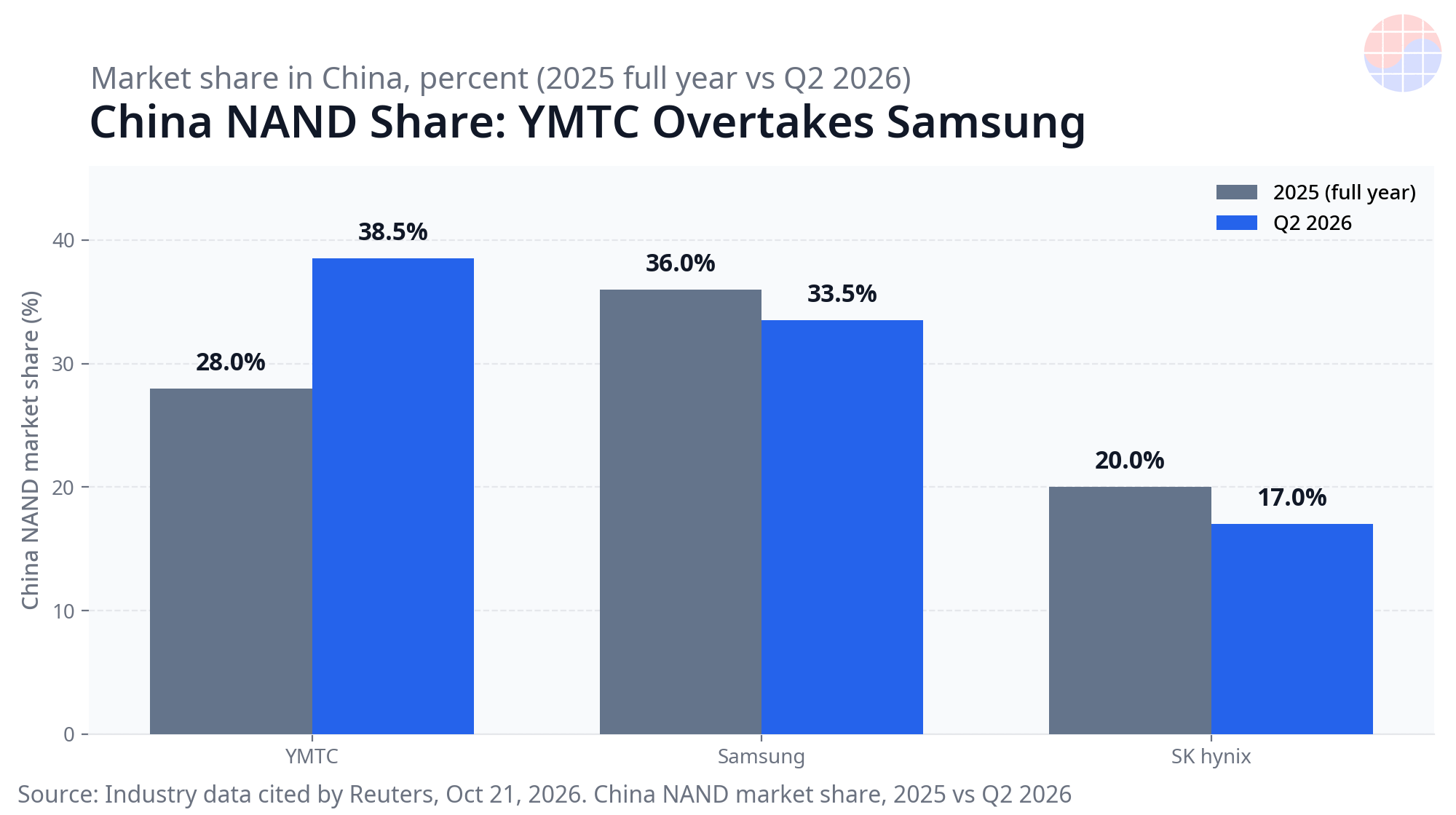
The market data explains why this is happening now. In 2025, Samsung still led China's NAND market with 36%, ahead of YMTC at 28% and SK hynix at 20%. By Q2 2026, YMTC had moved to 38.5%, Samsung had slipped to 33.5%, and SK hynix to 17% (industry data cited by Reuters, Oct 21, 2026). YMTC swung from 8 percentage points behind Samsung to 5 points ahead, a 13-point swing in roughly eighteen months (VLSI Korea calculation from industry data cited by Reuters, Oct 21, 2026).
YMTC's product position makes the share shift durable rather than accidental. Its lineup is mostly 160-layer and 232-layer NAND, with a small amount of 294-layer output, and it plans products above 300 layers (Reuters reporting, Oct 21, 2026). In other words, the Chinese competitor's mainstream products already sit at or above the layer counts the Korean China fabs are running today. The Korean fabs were not losing share to a cheaper legacy product. They were losing share while carrying a generational disadvantage in their own backyard market.
The honest qualification belongs here. A 286-layer Xi'an matches Samsung's current commercial frontier outside China, but it does not exceed YMTC's best silicon, which already reaches 294 layers in small volume. And outside China the frontier keeps moving: Samsung unveiled a prototype with more than 400 layers in August 2026 (Reuters reporting, Oct 21, 2026). The upgrades restore competitiveness. They do not end the race.
Chase's Take
Three judgments. First, the wording is the strategy. Both companies confirmed the upgrades are underway in close consultation with Washington, and Samsung pre-emptively defined the work as compliant, demand-driven, and not an expansion (company statements to Reuters, Oct 21, 2026). In a licence regime that distinguishes operating a fab from upgrading it, that framing is not public relations decoration. It is the permit strategy, stated in public.
Second, a layer conversion is an operations project before it is a headline. Raising a stack from about 200 to 286 layers means requalifying the highest-aspect-ratio etch and deposition steps in the fab, re-tuning defect control, and re-proving yield on a taller, less forgiving structure — inside a running fab that supplies about 40% of a global portfolio. Anyone who has lived through a process transfer knows the ramp profile, 5,000 wafers a month scaling to 40,000 over a year, is the sound of engineers being careful, not slow (Reuters reporting, Oct 21, 2026; ramp figures as reported).
Third, the real contest is cost per bit in China, and it is now symmetric. YMTC climbed to 38.5% share with 232-layer mainstream products against Korean fabs stuck near 200 layers (industry data cited by Reuters, Oct 21, 2026). Once Xi'an runs 286 layers and Dalian runs 240 layers and above, that structural excuse disappears. What remains is execution: yield, ramp discipline, and whether the licensing boundary holds for the full conversion schedule.*
Implications
- For Samsung, the Xi'an V9 conversion protects the economics of about 40% of its global NAND output and aligns the China fab with the 286-layer products it already sells from elsewhere (Reuters reporting, Oct 21, 2026).
- For SK hynix, Dalian at 240 layers and above supports Solidigm's enterprise SSD roadmap ahead of its planned US IPO, and the possible 300-layer research path keeps a US production option alive (Reuters reporting, Oct 21, 2026).
- For YMTC, the window in which its layer advantage over the Korean China fabs was structural is closing; its defence shifts to its 294-layer output, its planned 300-layer-plus products, and home-market momentum at 38.5% share (industry data cited by Reuters, Oct 21, 2026).
- For customers, more bits from the same fabs mean better high-density NAND supply for AI data-centre SSDs without waiting for new fab construction (Reuters reporting, Oct 21, 2026).
- For policymakers, the episode tests where operating an existing foreign fab ends and upgrading it begins — the exact line the Bureau of Industry and Security said it intends to police (Reuters reporting, Oct 21, 2026).
Note on limits: Reuters reported it could not determine the extent of licences granted for these upgrades, and neither company disclosed the detailed plans reported by Reuters; the licensing status of specific equipment moves should therefore be read as unconfirmed (Reuters reporting, Oct 21, 2026). This article is analysis based on Reuters reporting and company statements, not investment advice.
FAQ
Q1. What are Samsung and SK hynix upgrading in China, and why? A1. Samsung is converting its Xi'an NAND fab from about 200 layers to 286-layer V9 NAND, and SK hynix is switching its Dalian fab from 192 layers to 240 layers and above, to fend off YMTC and meet AI demand (Reuters reporting, Oct 21, 2026).
Q2. Is Samsung expanding NAND capacity in China? A2. No, by the company's own statement. Samsung told Reuters the Xi'an upgrade complies with US export regulations, meets growing global customer demand including in the US, and is not a capacity expansion and not a new facility (Samsung statement to Reuters, Oct 21, 2026).
Q3. How large is YMTC's lead in China's NAND market? A3. YMTC held 38.5% of China's NAND market in Q2 2026, ahead of Samsung at 33.5% and SK hynix at 17%, after trailing Samsung 28% to 36% in 2025 (industry data cited by Reuters, Oct 21, 2026).
Q4. Do the upgrades put the Korean fabs ahead of YMTC on technology? A4. Not outright. The upgrades close a one-generation gap to the current commercial frontier — Samsung sells up to 286 layers and SK hynix up to 321 layers outside China — while YMTC already ships a small amount of 294-layer NAND and plans products above 300 layers (Reuters reporting, Oct 21, 2026).
📩 Subscribe to VLSI Korea
Get our daily semiconductor deep-dives delivered to your inbox first. Free to subscribe.