VLSI Korea
Intel Inference GPU Deep Dive: Why the D270 Skips HBM for 480GB of LPDDR5X
Intel skipped HBM entirely: 160GB on its own card, up to 480GB in ODM designs. Verifying the viral 480GB figure, the capacity-over-bandwidth logic of inference, and what it means for Samsung, SK hynix and Micron.


The 30-Second Summary
On October 12, 2026, at the OCP Global Summit, Intel gave its inference-only GPU a commercial name and final specifications. Code-named Crescent Island, the product line is the Intel GPU D-Series, and its first card is the D270 (per trade-press reporting). The headline is the memory: this card uses no HBM at all. Twenty LPDDR5X packages deliver 1.5 TB/s of bandwidth, and while Intel's own card carries 160GB, ODM partner designs can scale capacity to 480GB. The "480GB of LPDDR5X" figure circulating in social-media analysis posts is real — but conditional: the card Intel itself sells ships with 160GB. Compute is 1.3 PFLOPS of FP8 in a 350W air-cooled PCIe card. Intel says a single card can serve models up to 300 billion parameters, and an eight-card system more than one trillion. Customer sampling is under way; pricing and a general-availability date have not been announced. This deep dive lays out every confirmed fact, the technical and economic logic behind "why LPDDR," and what it means for Samsung Electronics, SK hynix and Micron.
What Intel Actually Announced
Crescent Island did not appear overnight. Intel first unveiled the inference GPU at the OCP Global Summit in October 2025, disclosing a 160GB LPDDR5X configuration. At Hot Chips in August 2026 it walked through the Xe3P architecture in detail, and on October 12, 2026 it locked in the GPU D-Series brand and final specs. Intel also showed a liquid-cooled OAM prototype — two GPUs per module, eight modules in a 5U chassis — a signal that air-cooled PCIe is the beachhead while denser form factors stay on the roadmap.
The design philosophy has been consistent from the start: do not fight flagship training GPUs head-on. The target is not the HBM-based stronghold of NVIDIA's Blackwell Ultra or AMD's MI series, but the inference workloads that can run inside the standard x86 servers enterprises already own. Anil Nanduri, Intel's VP of AI products and go-to-market for the Data Center Group, put it plainly at the event: "Inference is becoming the defining AI workload, and enterprises need infrastructure that delivers the right performance at the right cost."
| Specification | Intel GPU D270 (Crescent Island) |
|---|---|
| Architecture | Xe3P (enhanced Xe3) |
| Xe cores | 32 (four slices) |
| XMX matrix engines | 256 |
| FP8 compute (dense) | 1.3 PFLOPS |
| FP64 vector compute | 10.2 TFLOPS |
| L2 cache | 32MB (unified) |
| Memory | LPDDR5X, 20 packages, 80 channels, 1,280-bit |
| Memory data rate | 9,375 MT/s |
| Memory bandwidth | 1.5 TB/s |
| Memory capacity | 160GB (Intel card) / up to 480GB (ODM designs) |
| Host interface | PCIe Gen5 x16 |
| Power | 350W |
| Form factor / cooling | Double-width PCIe CEM, air-cooled |
| Status | Customer sampling (Oct 2026); price and GA date not announced |
Source: Intel's October 12, 2026 OCP Global Summit disclosures and Hot Chips 2026 architecture materials.
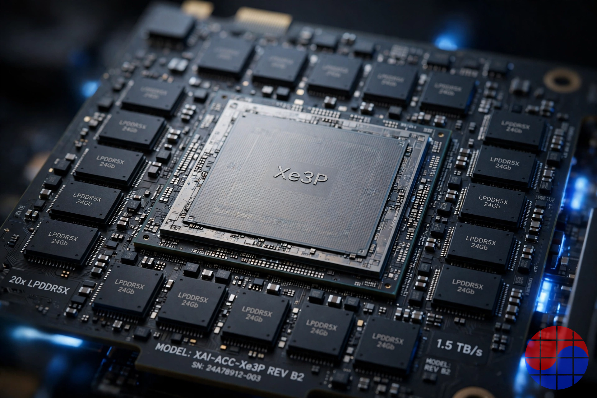
The Xe3P core itself was re-cut for inference. The XMX systolic array deepened from 4-deep in Xe2 to 16-deep, the general register file doubled to 1MB per core, and L1/shared local memory grew to 512KB per core. The 3D graphics and ray-tracing blocks found in gaming GPUs were removed entirely, giving every square millimeter to matrix math and inference data types from FP4 through FP64. Software is built around an open stack centered on OpenVINO and oneAPI.
Verifying 480GB: Real Number, Missing Footnote
After the announcement, "480GB of LPDDR5X" traveled through social analysis posts as if it were the card's headline spec. The number does appear in Intel's own disclosure — but it is the maximum configuration ODM partners can build, not the spec of Intel's branded card. Dropped of that footnote, the figure misleads.
| Configuration | Package density | Packages | Total capacity | Sold by |
|---|---|---|---|---|
| Intel reference card | 64Gb-class packages | 20 | 160GB | Intel (branded card) |
| ODM maximum | 192Gb-class packages | 20 | 480GB | Partner (ODM) boards |
The memory subsystem is identical in both: an 80-channel, 1,280-bit bus of 16-bit channels running at 9,375 MT/s for 1.5 TB/s. Only the number of DRAM dies stacked inside each package differs. So 480GB is "the ceiling the design allows," and 160GB is "what Intel actually ships." Either way, it sits at the top of the capacity class announced for a PCIe inference card. For comparison, NVIDIA's Rubin GPU carries 288GB of HBM4 and AMD's MI450 series is reported at 432GB — on raw capacity, the LPDDR design inverts the usual hierarchy.
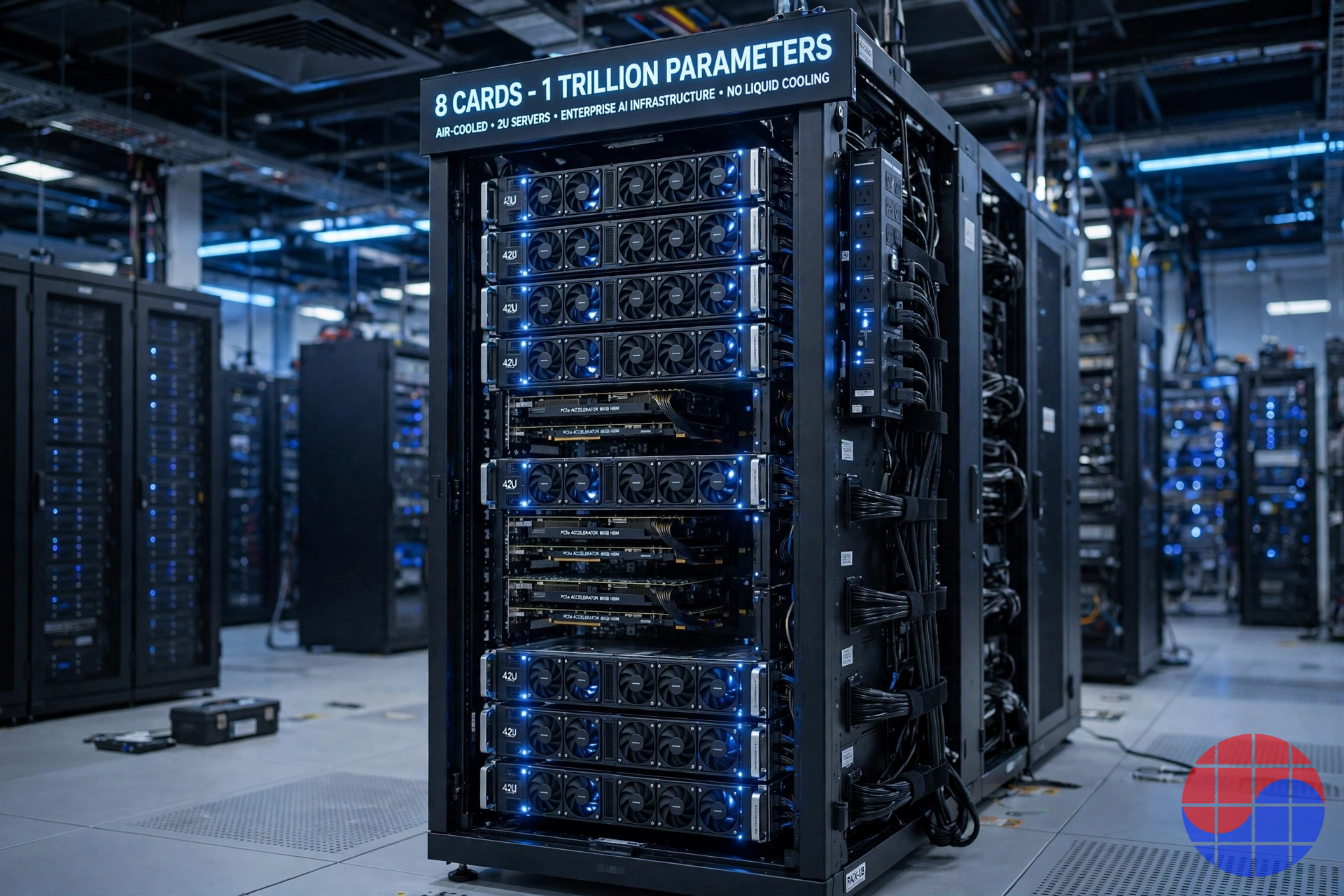
The model-size math needs the same care. At FP8 (one byte per parameter), a 160GB card holds roughly 160 billion parameters of weights before KV cache and runtime overhead; Intel's "300 billion parameters on a single card" maps to the 480GB configuration. The eight-card "more than one trillion parameters" claim likewise assumes 480GB × 8 = 3.84TB of pooled memory. The numbers are not false — but the reference configuration must always travel with them.
Why LPDDR5X (1): Inference Is Bottled Up by Memory, Not Math
Training and inference use memory differently. Training repeats enormous matrix multiplications, so both FLOPS and bandwidth matter. Inference — especially the decode phase that emits one token at a time — is a bandwidth game at small batch sizes: every token requires reading the model's entire weight set from memory once, so the time to stream the weights sets inter-token latency.
But in production serving, bandwidth is not the only wall. As concurrency rises and contexts lengthen, the KV cache eats memory fast. The binding constraint becomes: does the model fit on one card, and how many concurrent requests and how much context can that card hold? If capacity falls short, the model must be sharded across cards, and inter-card traffic and idle compute become pure cost. That is exactly Intel's bet. The D270 concedes bandwidth by an order of magnitude to HBM flagships, but multiplies capacity two- to three-fold at a fraction of the card price and power — and in that regime, cost per token wins.
The framing in numbers: 1.5 TB/s does not reach even a single HBM4 stack (2.8 TB/s and up), let alone the tens of TB/s of a 12-stack flagship. In exchange, the D270 is a 350W air-cooled card. Where HBM flagships push past 1,000W and force liquid-cooled racks, the D270 drops into an empty PCIe slot in an existing enterprise server. Intel is not selling peak performance; it is selling inference capacity that can be deployed today, in infrastructure that already exists.
Why LPDDR5X (2): Cost per GB and the Ability to Buy It at All
The second argument is money and supply. HBM4 is discussed at roughly $31–32 per GB — about double HBM3E's $17–18 per GB (industry estimates). LPDDR5X, even after supercycle price spikes, traded at roughly $12 per GB at the 12GB-package level — less than half of HBM4. Packaging widens the gap: HBM inherits the TSV-stacking and interposer bottleneck of advanced packaging capacity, while LPDDR5X is commodity DRAM consumed by hundreds of millions of phones and PCs each year, with a wide supplier pool and standard packaging.
Procurement risk is the 2026 reality. Samsung's and SK hynix's 2026 HBM output is effectively sold out, and Micron has reportedly pre-committed a large share of its 2027 supply. Joining the HBM queue today means waiting for 2027 allocation. LPDDR5X, by contrast, can be bought now. For a late entrant with low priority in the HBM allocation line, an "inference card without HBM" is both a cost cut and a hedge against procurement risk. Intel is not alone in reaching this conclusion: Meta's in-house MTIA inference chips have used LPDDR-class memory, and Tesla's inference silicon made the same family of choice.
Three Memories Compared: HBM4 vs LPDDR5X vs GDDR7
| Dimension | HBM4 | LPDDR5X | GDDR7 |
|---|---|---|---|
| Bandwidth per stack/chip | 2.8+ TB/s per stack | ~77 GB/s per package (1.5 TB/s per card) | Up to ~144 GB/s per chip |
| Total bandwidth per accelerator | Tens of TB/s (12 stacks) | 1.5 TB/s (D270) | ~1.8 TB/s (512-bit) |
| Capacity per accelerator | 288–432GB | 160–480GB | 32–96GB |
| Cost per GB | ~$31–32 (industry estimates) | ~$12 (at 2026 spike pricing) | Far below HBM (commodity graphics) |
| Power profile | High, incl. interposer system | Lowest energy per bit (mobile design) | Higher energy per bit than LPDDR |
| Packaging | TSV stack + interposer required | Standard packages, board-mounted | Board-mounted |
| Supply situation | 2026 output sold out; allocation race | Commodity DRAM; wide supplier pool | Contends with graphics demand |
| Key adopters | NVIDIA Rubin, AMD MI450 series, TPU/Trainium flagships | Intel GPU D-Series, NVIDIA Grace/Vera (CPU memory), Meta MTIA | GeForce RTX 50 series and other graphics cards |
Note: Cost-per-GB figures are estimates that vary widely by timing and contract terms; they are shown to illustrate direction — LPDDR5X at less than half of HBM4. Bandwidth figures follow each vendor's disclosed specifications.
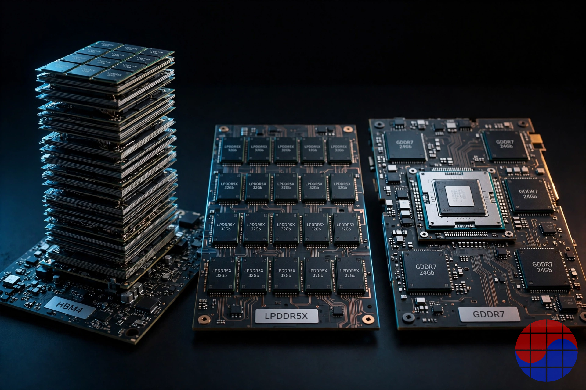
The table is not a ranking; it is a choice of which constraint to buy off. HBM4 buys bandwidth and accepts capacity cost and allocation risk. GDDR7 is cheap with respectable bandwidth, but its small per-chip capacity makes it hard to place hundreds of gigabytes on one card. LPDDR5X gives up bandwidth and wins on capacity cost, availability and power. As inference demand shifts from "the fastest token" to "the cheapest token," the center of gravity in this table tilts toward LPDDR.
What It Means for Suppliers: Samsung, SK hynix, Micron — and SOCAMM
For the three memory majors, the signal is simple: AI data-center DRAM demand is not converging on HBM alone. On the CPU side, large volumes already flow to LPDDR. NVIDIA's Grace carried up to 480GB of LPDDR5X per CPU; its successor Vera scales to 1.5TB at 1.2 TB/s through SOCAMM2 modules. A single Vera Rubin NVL72 rack holds 36 Vera CPUs — up to 54TB of CPU memory per rack. Add LPDDR accelerators like the D270, and data-center LPDDR grows from "memory next to the CPU" into an independent demand axis.
The modularization matters. LPDDR began as a soldered-down mobile component; NVIDIA's SOCAMM format redefined it as a serviceable, upgradeable server part. Samsung, SK hynix and Micron all participate in SOCAMM supply, and NVIDIA has reportedly added Taiwan's Nanya to the Vera LPDDR supply chain — diversification that itself signals how large the volume has become.
From a Korean supplier's seat, the demand is double-edged. On one side, a new AI-driven demand pool fills the commodity DRAM market that HBM conversion has been draining — server demand is part of why LPDDR5X prices jumped by double digits per quarter through 2026. On the other side, LPDDR remains commodity DRAM: no HBM-style excess margins, and direct price exposure to followers such as CXMT. Still, the direction of volume is unambiguous. From 2027 onward, LPDDR bit demand in AI infrastructure grows structurally from both CPU sockets and inference accelerators.
The Competitive Frame: Even NVIDIA Puts LPDDR Next to Its CPUs
Reading Intel's choice as merely "the fallback of a company that could not secure HBM" misses half the picture. NVIDIA — the largest HBM buyer on earth — itself runs a two-track memory strategy: HBM4 on the GPU, LPDDR5X on the CPU, splitting bandwidth-hungry and capacity-hungry roles by workload. From Grace to Vera, CPU memory capacity tripled from 480GB to 1.5TB and bandwidth rose from 512 GB/s to 1.2 TB/s; in NVIDIA's view, the agentic-AI-era CPU is a part that must wear more memory, not less.
AMD holds the opposite flank: the MI series keeps the orthodox HBM-everywhere line and fights inference on bandwidth. Custom ASICs split both ways — Google's TPU and AWS Trainium take HBM, Meta's MTIA takes LPDDR-class memory. The industry's emerging consensus is a two-story structure: HBM for training and frontier serving; LPDDR growing underneath, in mass inference and CPU memory. The D270 is the first full-scale attempt to attack that lower story in a GPU form factor.
Chase's Take
Strip the branding away and this product is a memory procurement strategy wearing a GPU costume. Intel avoided a compute fight it cannot win and shipped the largest inference capacity that can be built from memory that is actually purchasable in 2026–2027. The 1.3 PFLOPS figure is unremarkable; the combination — 480GB on a 350W air-cooled card — is a coordinate no rival occupies.
For Korean memory makers, this is a quiet tailwind. Behind HBM's glamorous pricing, a second AI demand axis — server LPDDR — is hardening into real volume. Once Vera's 1.5TB per socket and the D270's up-to-480GB per card ship side by side, LPDDR5X gets repriced from a smartphone component into AI infrastructure. The catch: rising LPDDR prices gnaw at Intel's own TCO logic. The more expensive LPDDR becomes, the thinner the margin of the "cheap memory, cheap inference" equation. This product's fate will be decided less by its silicon than by the memory price curve.
For the cost structure of inference memory read against the HBM camp's own numbers, see also: No HBM Needed? Intel's 480GB LPDDR5X Bet and the Inference Memory TCO War
Risks and What Is Not Yet Known
First, the nature of the performance figures: 1.3 PFLOPS is a theoretical peak with no independent benchmarks yet, and real token throughput depends heavily on kernel optimization and stack maturity. Second, the software ecosystem: CUDA's gravity is strong in inference too, and how smoothly the OpenVINO/oneAPI stack plugs into production serving frameworks will gate adoption — Intel's Gaudi line lost on ecosystem more than on silicon, a precedent that cannot be ignored. Third, the bandwidth ceiling: 1.5 TB/s can bottleneck high-batch decode of very large models, and Intel itself draws the line at training and frontier serving. Fourth, the commercial terms are blank: no price, no GA date, with volume shipments discussed for 2027 — by then HBM4E will have arrived and LPDDR prices may have climbed further, redrawing the competitive map. Finally, the market's first reaction was cool: Intel's shares were reported to close lower on the announcement day.
FAQ
Q: Is the D270's 480GB of LPDDR5X a confirmed specification? A: It is real as a maximum configuration, but Intel's own card carries 160GB. The 480GB figure is the ceiling for ODM boards populated with higher-density (192Gb-class) packages. Most social-media citations of "480GB" drop that condition.
Q: Why use LPDDR5X instead of HBM in an inference GPU? A: Because production inference is constrained less by raw compute than by the capacity to hold the model and KV cache, and by cost per token. LPDDR5X is discussed at less than half the cost per GB of HBM4, is far easier to procure, and draws less power. The design surrenders peak bandwidth to win on capacity and cost.
Q: How does the D270's 1.5 TB/s of bandwidth rate? A: Below a single HBM4 stack (2.8 TB/s and up) and an order of magnitude below flagship accelerators in the tens of TB/s — but in the same band as a 512-bit GDDR7 configuration (~1.8 TB/s). It is a figure built to compete on capacity per watt and per dollar, not on absolute throughput.
Q: What does this mean for Samsung Electronics and SK hynix? A: It signals that AI data-center LPDDR demand is expanding from server CPUs (NVIDIA Grace and Vera's SOCAMM) into inference accelerators. Margins will not match HBM, but structural volume growth is in view, and both Korean makers are inside the SOCAMM supply chain.
Q: When can the D270 be bought, and at what price? A: As of October 2026 the part is in customer sampling. Intel has not disclosed pricing or a general-availability date; volume shipments are discussed for 2027.
📩 Subscribe to VLSI Korea
Get our daily semiconductor deep-dives delivered to your inbox first. Free to subscribe.