VLSI Korea
The Math of Vera Rubin Production: 576 HBM4 Stacks per Rack, 300,000 Wafers per Million GPUs (TSMC, SK hynix, Samsung, Micron)
Jensen Huang declared Vera Rubin in full production in Berlin. The ramp, dissected in numbers: 576 HBM4 stacks and about 21.5 wafers per rack, 11,000-21,000 racks in 2027, the TSMC/SK hynix/Samsung/Micron supply map, and the bottleneck verdict.


The one-line conclusion — Vera Rubin's production speed is set not by GPUs but by HBM4 bits. In a structure where one rack consumes 576 HBM4 stacks and more than 21 wafers, the ceiling on the 2027 ramp is drawn by the memory makers' wafers.
30-Second Summary
- On October 21, 2026, at the GTC Berlin keynote, CEO Jensen Huang declared that Vera Rubin is "now in full production." Node assembly time fell from two hours for Grace Blackwell to under five minutes, and cooling is 100% liquid.
- One NVL72 rack holds 72 Rubin GPUs, 36 Vera CPUs, and 576 HBM4 stacks (20.7 TB = 165,888 Gb). Per GPU, HBM4 is eight 36 GB 12-high stacks, 288 GB (2,304 Gb).
- Volumes exist only as estimates. The market's current base case is 5,000–7,000 racks in H2 2026 (supply-chain estimates) and 11,000–21,000 racks in 2027 (0.8–1.5 million GPUs).
- Converted to wafers, one GPU consumes 0.037 logic wafers + 0.143 CoWoS wafers + 0.118 HBM DRAM wafers — roughly 0.30 wafers in total. One million GPUs means roughly 300,000 wafers.
- Bottleneck verdict: first, HBM4 (2026 volume effectively spoken for, reported allocation trims, a steep 2027 contract-price outlook); second, CoWoS. Logic wafers and rack assembly are not constraints.
1. The Berlin Declaration — Confirmed Facts First
On October 21, 2026, Jensen Huang held up a Vera Rubin node at the GTC Berlin keynote and confirmed three things. First, Vera Rubin is now in full production. Second, node assembly time has dropped from two hours in the Grace Blackwell generation to under five minutes — a result of eliminating cables and wires. Third, cooling is 100% liquid, up from 80% liquid in the prior generation, with a 45°C coolant inlet temperature.
Production itself was not news. NVIDIA announced production entry at CES in January 2026, and its May 31 GTC Taipei release set production shipments for the fall. On June 1, cloud operator CoreWeave completed bring-up of the first NVL72 rack and confirmed live operation. What Berlin confirmed is that "in production" now means a full ramp, not samples and early units. Huang also noted that 150 Taiwanese supply-chain partners stand behind Vera Rubin.
This article takes that declaration apart in numbers: how many systems get built, what goes into one rack and in what quantity, how that volume converts into wafers, and which company supplies what, and how much. Figures from official disclosures and reporting carry their sources; figures derived by calculation are labeled estimates with their assumptions shown.
2. Anatomy of One Rack — Inside the NVL72
Vera Rubin's unit of sale is not a GPU chip but a rack. One NVL72 consists of 18 compute trays and 9 NVLink switch trays, with 72 GPUs bound by the NVLink 6 fabric into what behaves like a single giant accelerator.
| Component | Quantity / Spec | Notes |
|---|---|---|
| Rubin GPU | 72 | 336B transistors per GPU (two dies), TSMC 3nm |
| Vera CPU | 36 | 88-core Arm, NVLink-C2C to the GPUs |
| HBM4 | 576 stacks, 20.7 TB | 8 stacks × 36 GB per GPU |
| LPDDR5X (for CPU) | Up to 54 TB | Up to 1.5 TB per CPU, SOCAMM2 modules (per brokerage analysis) |
| NVLink 6 fabric | 260 TB/s per rack | 3.6 TB/s per GPU |
| Networking | ConnectX-9 NICs, BlueField-4 DPUs | Scale-out via Spectrum-X Ethernet |
| Cooling | 100% liquid | 45°C coolant inlet |
| Power draw | ~190–230 kW | Supply-chain estimates |
| Rack price | $5M–$7.8M | March 2026 reporting and brokerage BOM analysis |
Source: NVIDIA's published NVL72 specifications, GTC Berlin 2026 keynote coverage (October 21, 2026), brokerage bill-of-materials analysis.
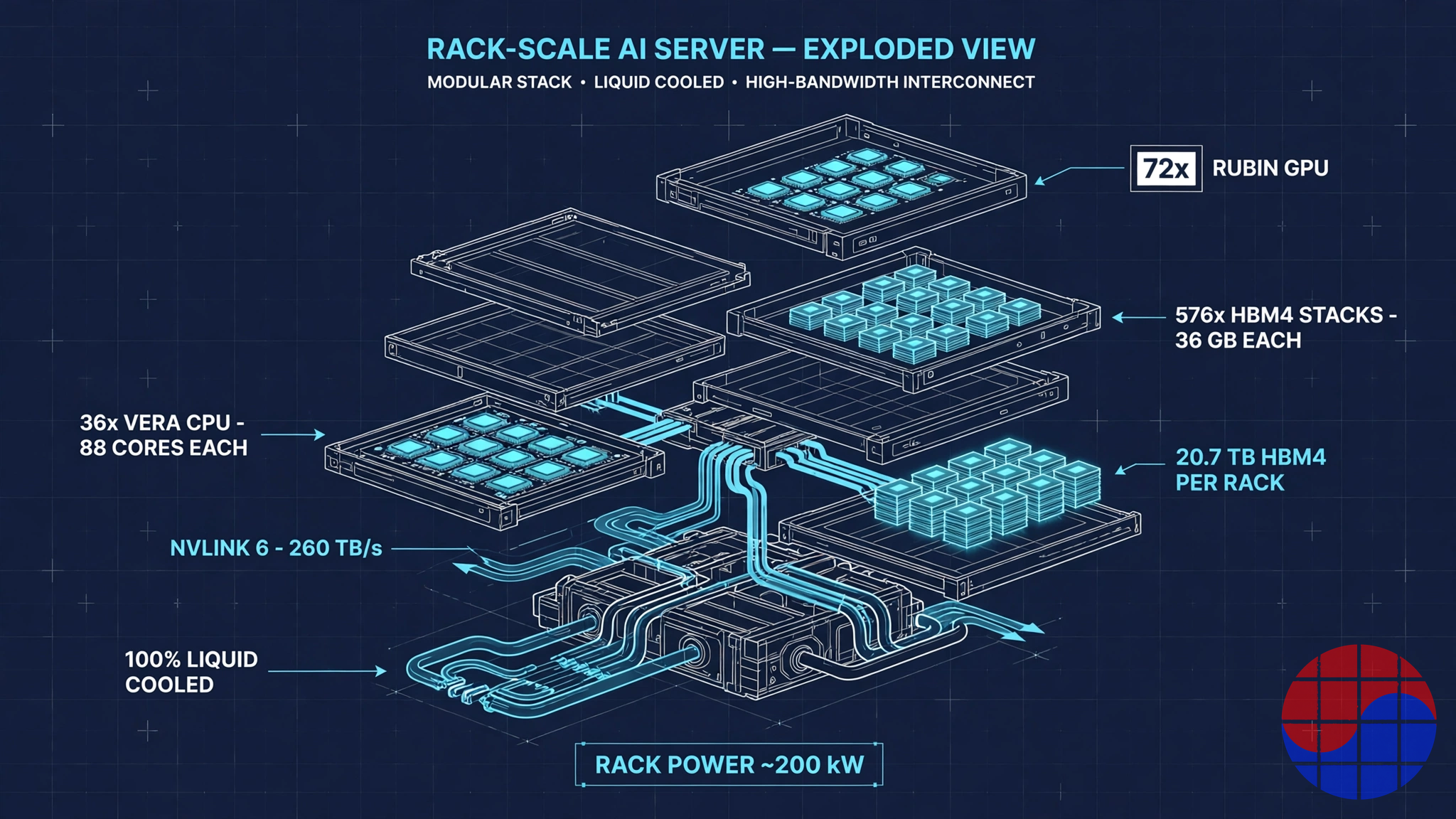
Anatomy of a Vera Rubin NVL72 rack — 72 GPUs and 576 HBM4 stacks in a single rack. Source: VLSI Korea
The HBM4 Arithmetic
This platform is, at its core, a memory system. Unpacking one GPU's HBM4 in bits:
| Item | Value | Math |
|---|---|---|
| One HBM4 stack | 36 GB (288 Gb) | Twelve 24 Gb dies stacked |
| Stacks per GPU | 8 | NVIDIA specification |
| HBM4 per GPU | 288 GB (2,304 Gb) | 8 × 36 GB |
| Bandwidth per GPU | 22 TB/s | NVIDIA specification |
| Stacks per rack | 576 | 72 × 8 |
| HBM4 per rack | 20.7 TB (165,888 Gb) | 72 × 288 GB |
| HBM DRAM dies per rack | 6,912 | 576 stacks × 12 dies |
Against Blackwell, HBM capacity per GPU rose 1.5×, from 192 GB to 288 GB, and bandwidth 2.75×, from 8 TB/s to 22 TB/s. The stack count stayed at eight, but each stack grew from 24 GB to 36 GB and pin speeds climbed. What matters for production is that the entire capacity increase is billed in additional DRAM wafers: every stack requires twelve 24 Gb dies, and accounting for die yield, actual wafer consumption runs higher still.
3. How Many Get Built — Volume Scenarios
NVIDIA does not disclose Rubin unit shipments. Every number in circulation is an estimate, and this article uses only those with transparent methods.
Back-Solve 1: From Revenue
Market discussion, grounded in NVIDIA's guidance and executive commentary, contemplates a run-rate where Vera Rubin contributes roughly $20 billion in quarterly revenue. Dividing by the reported rack price range ($5M–$7.8M) yields 2,550–3,975 racks per quarter, or roughly 10,000–16,000 racks annualized. Note that this back-solve assumes all Rubin revenue comes from NVL72 racks, making it an upper-bound reference — board- and module-level sales and parallel Blackwell revenue are mixed in, in reality.
Back-Solve 2: Supply-Chain Estimates
Analysts tracking the Taiwanese supply chain put H2 2026 VR200 rack shipments at 5,000–7,000 units (reported as Ming-Chi Kuo's estimate), which converts to 360,000–500,000 GPUs. With reported HBM4 allocation trims in the mix, a parallel consensus puts total 2026 Rubin GPUs at 250,000–350,000. For 2027, the scaling year, the base scenario is 0.8–1.5 million GPUs (11,000–21,000 racks). Industry estimates also project NVL72-class rack shipments overall (GB300 + VR200 + VR300) growing more than 50% year over year in 2027, with VR200 taking the largest share.
| Period | Racks (est.) | GPUs (est.) | HBM4 stacks (est.) | Basis |
|---|---|---|---|---|
| H2 2026 | 3,500–7,000 | 250K–500K | 2.0M–4.0M | Supply-chain estimates; fall shipment start |
| Per quarter at ramp peak | 2,550–3,975 | 180K–290K | 1.47M–2.29M | Back-solve from ~$20B quarterly revenue |
| 2027 | 11,000–21,000 | 0.8M–1.5M | 6.4M–12.0M | Base-scenario range |
Every figure in this table is an estimate, not a confirmed number. What is confirmed is production itself, and the fall start of shipments.
Converted to HBM4 bits, the picture changes scale. Even the low end of the 2027 base case (0.8 million GPUs) requires 230 PB (230,400 TB) of HBM4; the high end (1.5 million GPUs) reaches 432 PB. A single platform absorbs a substantial share of the world's entire HBM output.
4. The Wafer Conversion — One GPU = 0.30 Wafers
Converting volume into wafers reveals where the bottleneck sits. The model below is our own, with every assumption disclosed; read the outputs as ranges.
Assumptions
| Wafer type | Assumption | Result |
|---|---|---|
| Logic (TSMC 3nm) | Die area ~800 mm² × 2 (near the 858 mm² reticle limit), ~65 gross dies per 300 mm wafer, 85% die yield | ~55 good dies per wafer = ~27 GPUs |
| CoWoS packaging | Package footprint ~4,700 mm² (2026's 5.5-reticle class), 6–8 packages per wafer | ~7 GPUs per wafer |
| HBM4 DRAM | 24 Gb die ~60 mm², ~1,090 gross dies per wafer, 75% effective KGD/stacking yield | ~820 dies per wafer = ~8.5 GPUs |
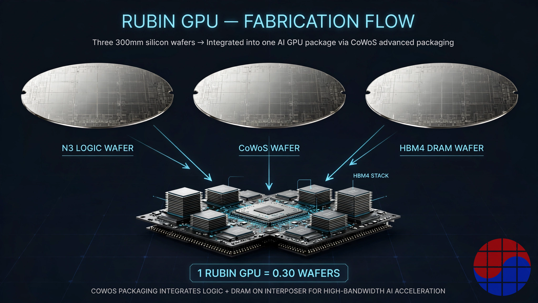
The three wafer types one GPU consumes — logic, CoWoS, and HBM DRAM. Source: VLSI Korea
Conversion Results
| Category | Per GPU | Per rack (72 GPUs) | 2027 (0.8M–1.5M GPUs) |
|---|---|---|---|
| Logic wafers (3nm) | 0.037 | ~2.7 | 30K–56K |
| CoWoS wafers | 0.143 | ~10.3 | 114K–214K |
| HBM4 DRAM wafers | 0.118 | ~8.5 | 94K–176K |
| Total | ~0.30 | ~21.5 | ~240K–450K |
The takeaway is unambiguous. Building one million GPUs takes roughly 300,000 wafers across the three types, and close to 90% of them are packaging (CoWoS) and memory (DRAM) wafers. Pure logic wafers are only about 12% of the total. Reporting likewise indicates that the top four AI chip designers consume only about 12% of leading-edge logic output — which is precisely why logic fabs are not the constraint on the AI ramp.
Set against supply: TSMC reaches an estimated 120,000–150,000 CoWoS wafers per month by end-2026, and with OSAT partner capacity the industry total approaches roughly 200,000 per month. NVIDIA reportedly pre-booked about 60% of TSMC's 2026 CoWoS. Rubin's 2027 CoWoS requirement (114K–214K wafers per year) is a single-digit percentage of TSMC's annual capacity, so the arithmetic works even shared with Blackwell — the catch is package growth: as package footprints expand, packages per wafer fall, and expansion keeps getting eaten by area.
5. The Supplier Map — Who Supplies What, and How Much
Behind one Vera Rubin rack stand hundreds of suppliers, including the 150 Taiwanese partners Huang cited. The core map:
| Company | What it supplies | Volume / role |
|---|---|---|
| TSMC | 3nm GPU dies, CoWoS-L packaging | All GPU dies. NVIDIA reportedly booked ~60% of 2026 CoWoS capacity |
| SK hynix | HBM4, SOCAMM2 LPDDR5X | Mid-50% range of initial HBM4 allocation (reported). 12-high 36 GB stacks; SOCAMM2 shown for Vera CPU |
| Samsung | HBM4 | Mid-20% range of initial allocation (reported). 1c DRAM + 4nm base die; fastest spec at up to 3.0 TB/s per stack, 11.7 Gbps. HBM4E samples target Rubin Ultra |
| Micron | HBM4 | ~20% of initial allocation (reported). 36 GB 12-high in high-volume shipment since Q1 2026; >2.8 TB/s per stack |
| Ibiden, Shinko, Unimicron, Nan Ya PCB | ABF substrates | Build-up substrates for 5.5-reticle-class packages; substrate area is capacity |
| ASE, Amkor | Back-end (CoWoS overflow) | An estimated 50K–60K WPM of new OSAT capacity absorbs TSMC overflow |
| Foxconn, Quanta, Wistron, Inventec | Rack assembly & integration | Foxconn cited as the largest assembler; the 5-minute node design sets throughput |
| Dell, HPE, Lenovo, Supermicro, GIGABYTE | System delivery | Complete racks to CSPs and enterprises |
| Vertiv, Schneider Electric, Delta | Power & cooling | CDUs and power for ~200 kW racks; DSX POD partners |
| NVIDIA (in-house) | ConnectX-9, BlueField-4, NVLink switches, Spectrum-X Photonics | Rising in-house BOM share — NVIDIA's take of rack revenue grows each generation |
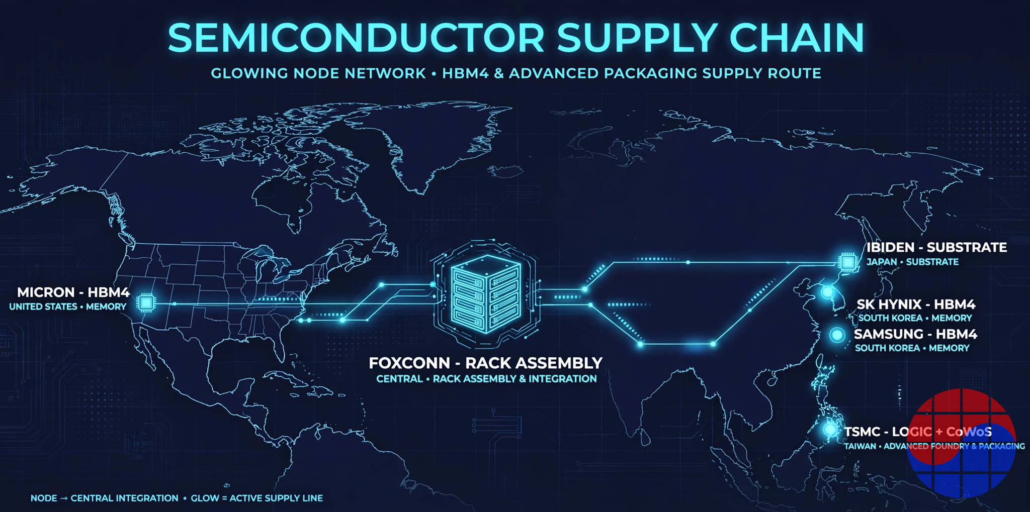
The Vera Rubin supply chain — logic and packaging in Taiwan, HBM4 split between Korea and the US, substrates in Japan. Source: VLSI Korea
The HBM4 allocation rests on reporting of NVIDIA's late-2025 volume assignments: SK hynix largest in the mid-50% range, Samsung in the mid-20% range, Micron around 20%. This split is not fixed. Samsung began the industry's first HBM4 mass-production shipments in February 2026 and leads on speed specifications, while reporting in April indicated SK hynix weighed trimming its 2026 HBM4 shipments to NVIDIA by 20–30% amid ramp timing — a structure in which quarterly allocations can move.
Rack assembly economics changed, too. With node assembly down from two hours to five minutes, assembly capacity is no longer a labor problem but a parts-arrival problem. For assemblers, Vera Rubin is a rack that ships at the speed parts arrive — meaning HBM4 and finished CoWoS packages set line utilization. Our companion piece on NVIDIA's modular AI factory design, the Vera Rubin DSX POD deep dive, covers deployment speed; this article focuses on how many systems get built, and from how many wafers.
6. Bottleneck Verdict — What Actually Gates the Ramp
| Process | Verdict | Evidence |
|---|---|---|
| HBM4 | The primary constraint | 2026 volume effectively sold out. Reported shipment-trim review. A 12-high 36 GB stack projected to rise from ~$600 in 2026 to ~$1,300 in 2027 (contract price +121% YoY estimate, reported) |
| CoWoS | Tight, manageable | Capacity up ~8× in three years, but package-area growth offsets expansion. Industry supply shortfall of 10–20% persists in estimates |
| ABF substrates | Watch | Directly exposed to large-package area growth; has quietly bottlenecked before |
| 3nm logic wafers | Not a constraint | Top-4 AI designers consume ~12% of leading-edge logic output (reported) |
| Rack assembly | Not a constraint | 5-minute node assembly, modular design; the constraint is parts arrival |
| Power & sites | A customer-side constraint | 190–230 kW per rack; 800VDC transition and liquid-cooling infrastructure are site challenges |
The conclusion is simple. Vera Rubin's production function reads min(HBM4 stacks ÷ 576, CoWoS packages ÷ 72, logic dies ÷ 144), and in 2026–2027 the term that sets the minimum is HBM4. If Rubin's revenue misses guidance in an NVIDIA earnings print, suspect HBM4 deliveries before demand. Conversely, if HBM4 contract prices really do near-double in 2027, that is the signal the memory trio has begun collecting its share of the ramp's economics.
Chase's Take
With all the numbers laid out, Vera Rubin is less a GPU product than the physical form of a memory purchasing contract. Of a rack's $5M–$7.8M price, the GPU dies' own wafer cost is a smaller share than intuition suggests; the money and the capacity are locked up in 576 HBM4 stacks and CoWoS area.
From a Korean vantage point, watch the slope of the allocation. SK hynix's mid-50% range is continuity from the Blackwell generation, but Samsung's mid-20% range looks like a floor for a comeback — if its speed and HBM4E cards play at the 2027 allocation reset, the slope changes. And what decides that slope is not marketing; it is quarter-by-quarter KGD yield and stacking throughput.
Finally, the 0.30-wafer figure is worth remembering. AI accelerator competition is now simultaneously a design contest and an allocation contest over three wafer types. TSMC's roadmap, pointing to HBM5 and 14-reticle-class packages for the next generation, says this allocation contest does not end — it only gets more expensive.
Sources: NVIDIA's published specifications and GTC Berlin 2026 keynote coverage (October 21, 2026), Korean and international supply-chain and earnings reporting, brokerage bill-of-materials analysis. Volume and wafer conversions are our own estimates under the stated assumptions and may differ from actual shipments. This article is not investment advice.
FAQ
Q: How many HBM4 stacks go into one Vera Rubin rack? A: 576. Each GPU carries eight 36 GB 12-high stacks (288 GB), and a rack holds 72 GPUs, so 72 × 8 = 576 stacks — 20.7 TB (165,888 Gb) in total.
Q: How many Vera Rubin systems will be produced in 2027? A: There is no confirmed figure. Combining supply-chain estimates and revenue back-solves, the base scenario for 2027 is 11,000–21,000 racks, or 0.8–1.5 million GPUs. H2 2026 is estimated at roughly 3,500–7,000 racks.
Q: How many wafers does it take to build one GPU? A: About 0.30 wafers across three types: 0.037 of a 3nm logic wafer, 0.143 of a CoWoS wafer, and 0.118 of an HBM4 DRAM wafer — our own estimate under the assumptions disclosed in this article (die area, yields, package footprint). Per rack, that is about 21.5 wafers.
Q: What is the real bottleneck in Vera Rubin production? A: HBM4. The 2026 volume is effectively spoken for, and reported shipment-trim reviews plus a steep 2027 contract-price outlook support that verdict. CoWoS is tight but expanding; 3nm logic wafers and rack assembly are hard to call constraints.
Q: Which companies supply the HBM4, and in what shares? A: Per late-2025 allocation reporting, SK hynix holds the mid-50% range, Samsung the mid-20% range, and Micron around 20%. Samsung brings the industry's first mass-production shipments (February 2026) and the fastest specifications, SK hynix the largest allocation and SOCAMM2, and Micron high-volume shipments since Q1 2026 — and allocations can be adjusted quarter to quarter.
📩 Subscribe to VLSI Korea
Get our daily semiconductor deep-dives delivered to your inbox first. Free to subscribe.