VLSI Korea
TSMC Kumamoto Fab 2 Moves to 3nm: Japan Certification, Subsidy and 2028 Production Plan
METI certified JASM Kumamoto Fab 2's switch to 3nm on October 16, 2026: 6,000 wafers per month, a JPY 645.15 billion maximum subsidy, and production by December 2028.


Conclusion: On October 16, 2026, Japan's Ministry of Economy, Trade and Industry (METI) certified a revised production plan for JASM, TSMC's Japanese subsidiary, in Kumamoto. Fab 2 will switch from 6nm and 12nm to 3nm logic, with production starting by December 2028. It is the first plan to produce 3nm semiconductors in Japan.
The certified capacity is 6,000 wafers per month (300mm equivalent). That is smaller than the original 48,000 wafers per month, but it is a first phase that prioritizes the process generation over volume. First shipments are expected in the fourth quarter of 2028, production is planned to continue for more than 10 years, and deliveries will center on Japanese customers.
What the certified plan says
| Item | Original plan (certified Feb 2024) | Revised plan (certified Oct 16, 2026) |
|---|---|---|
| Fab 2 main product | 6nm and 12nm logic, with 40nm also supported | 3nm logic |
| Capacity | 48,000 wafers per month | 6,000 wafers per month |
| Capex in certified plan | USD 12.2 billion | USD 10.8 billion |
| Maximum subsidy | JPY 732 billion | JPY 645.15 billion |
| Production start | - | By December 2028, first shipment in Q4 2028 |
Source: EE Times Japan (published October 19, 2026) and Reuters (October 16, 2026), reporting the METI certification. The stated reason for the change is the large shift in the market environment driven by the rapid advance of AI.
Fab 1 was revised on the same day
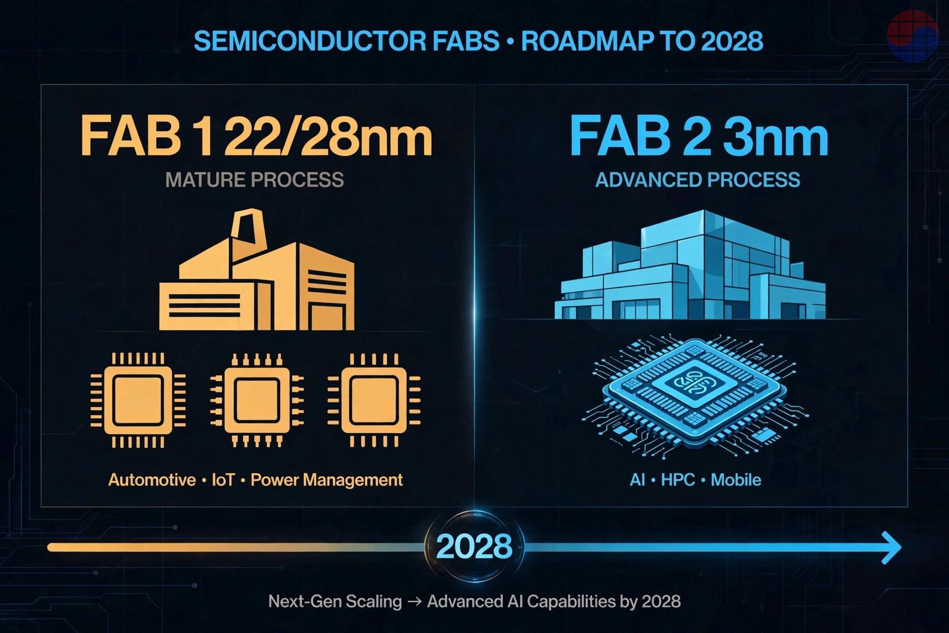
The production plan for Kumamoto Fab 1 was also revised and certified on the same day. Its main products become 22nm and 28nm logic, 12nm and 16nm are no longer listed as main products, and 40nm will also be produced in light of domestic demand. Total Fab 1 capacity changes from 55,000 to 50,000 wafers per month, and capex changes from USD 8.6 billion to USD 7.3 billion.
In other words, Kumamoto is now organized so Fab 1 covers mature nodes for automotive and industrial use, while Fab 2 covers the advanced node for AI.
Why is capacity only 6,000 wafers per month
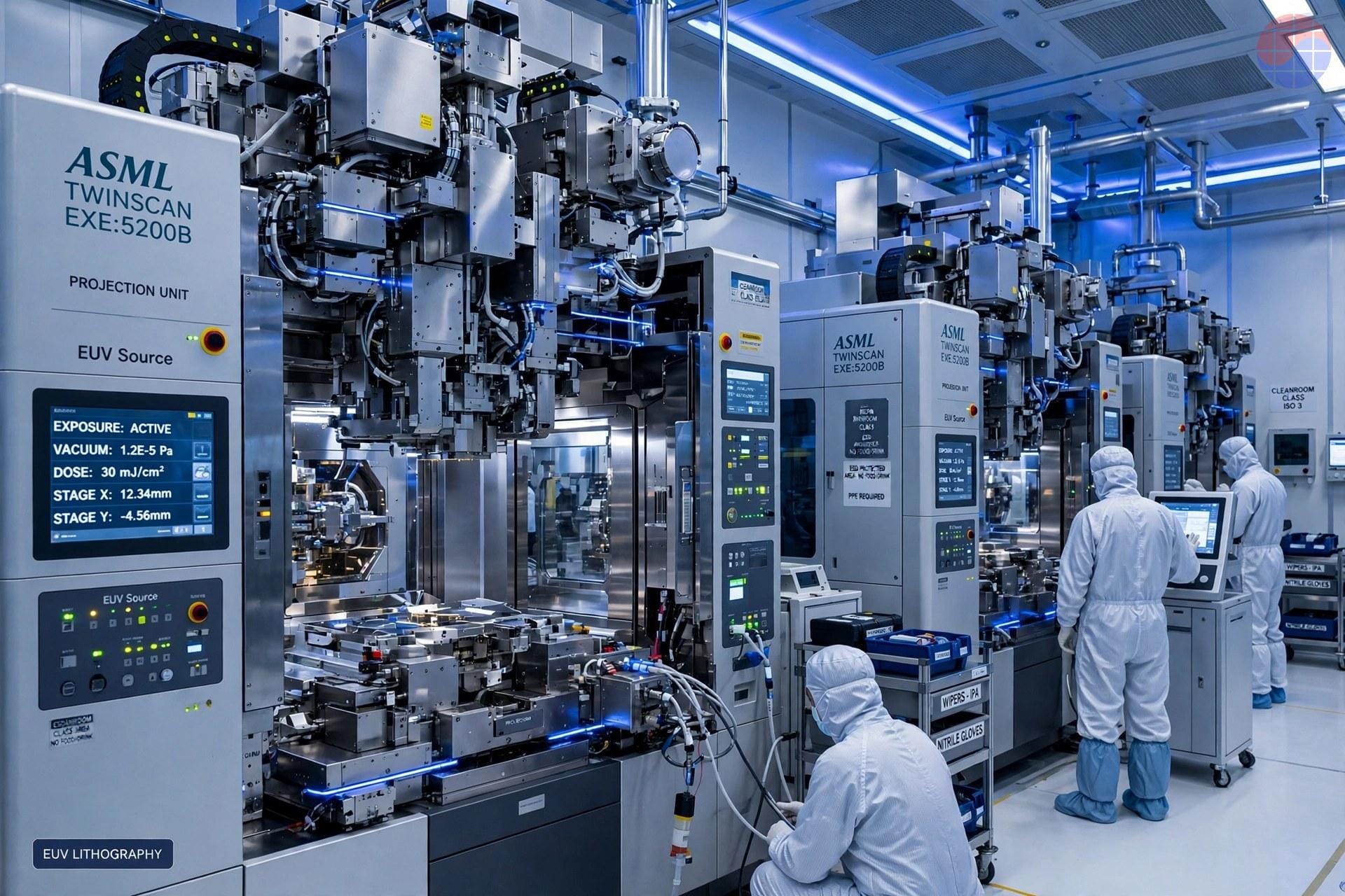
Producing 3nm requires EUV lithography tools. Installing those tools, bringing them up, and stabilizing yield takes time. The 6,000 wafer figure should be read as the certified first phase, not the final size.
Reports including Nikkei say total investment is expected to expand to at least USD 15.7 billion with the move to 3nm, and that final capacity will be decided according to additional support from the Japanese government. METI is at the stage of requesting support funds in its fiscal 2027 budget, so the scale of any expansion depends on upcoming budget and subsidy decisions.
TSMC chairman says the schedule is on track
At the earnings briefing on October 15, 2026, TSMC chairman and CEO C. C. Wei said the plan to introduce the 3nm process at the second Japan fab is progressing smoothly and that mass production is planned for 2028. The 3nm direction itself had been disclosed in February 2026, when Wei visited the Prime Minister's office.
According to Reuters, TSMC commented that combined capex for Fab 1 and Fab 2 in Kumamoto is expected to exceed USD 23 billion.
What it means for Japan
- Domestic supply: A domestic production base for the 3nm logic that underpins AI has taken concrete form for the first time.
- Economic security: METI says securing a 3nm production base in Japan is significant for supply chain resilience and economic security.
- Equipment and materials: An advanced fab ramp connects directly to demand for Japanese semiconductor equipment and materials. This certification is a production plan certification, however, and does not mean orders for individual companies have been decided.
- Jobs and hiring: Tool installation, bring-up, and mass-production build-out will proceed toward the 2028 start, one background factor behind continued hiring demand for semiconductor engineers centered on Kumamoto.
Rapidus, aiming for 2nm mass production in Hokkaido, targets a start in the second half of fiscal 2027. With 3nm in Kumamoto alongside 2nm in Hokkaido, advanced logic production in Japan moves from a single site to a multi-site structure.
Frequently asked questions
When will TSMC Kumamoto Fab 2 start 3nm production
Under the certified plan, production starts by December 2028, with first shipments expected in the fourth quarter of 2028.
How large is the capacity
The certified plan is 6,000 wafers per month (300mm equivalent). Final capacity is reported to be considered according to additional subsidies.
How large is the subsidy
The maximum subsidy for Fab 2 is JPY 645.15 billion, down from JPY 732 billion in the original plan. Additional support is at the fiscal 2027 budget request stage.
What will Fab 1 produce
After the revision, its main products are 22nm and 28nm logic, and 40nm will also be produced according to domestic demand.
Sources: EE Times Japan (October 19, 2026), Reuters (October 16, 2026), and Jiji Press (October 15, 2026) on the METI certification. The expanded total investment outlook is based on reports including Nikkei.
📩 Subscribe to VLSI Korea
Get our daily semiconductor deep-dives delivered to your inbox first. Free to subscribe.