VLSI Korea
Microsoft's Maia 300: The 1-Million-Chip Bet That Changes the AI Chip Business
Microsoft unveiled Maia 300, its third-generation custom AI chip, and plans to deploy over a million in 2027. The world's biggest GPU buyer is becoming a GPU competitor — and token economics, not FLOPS, is the new battleground.


The most important chip announcement of October 2026 is not about a faster accelerator. It is about who gets to be a chip company. On October 12, 2026, Microsoft unveiled Maia 300, the third generation of its in-house AI silicon, and said it plans to deploy potentially more than one million of them in 2027 as the primary inference system for its own products and services (Reuters, October 16, 2026). The world's largest buyer of AI GPUs is now, at the margin, becoming a GPU competitor — and every inference query that moves to Maia is spending that no longer passes through NVIDIA.
The specs are serious on their own: a chiplet package with compute dies on TSMC 2-nanometer-class silicon, eight HBM4 stacks delivering 288 GB of memory at 18.0 TB/s of peak bandwidth, inside a 950-watt envelope, assembled into 96-accelerator racks drawing about 167 kilowatts (Microsoft technical disclosure, October 12, 2026). Microsoft claims roughly 40% more tokens per megawatt than leading GPU-based systems and up to seven times the rack-level token throughput of its predecessor, Maia 200. But the strategic story is bigger than any benchmark: Microsoft is vertically integrating the most expensive layer of the AI stack — inference — and doing it at a scale that rewires the economics for foundries, memory makers, and merchant chip vendors alike.
What Microsoft actually announced
The announcement came via a blog post from Scott Guthrie, executive vice president of Cloud and AI, on Monday, October 12, 2026. CEO Satya Nadella called it Microsoft's "biggest bet yet on our own silicon," saying the company will scale the Maia family to multi-gigawatt deployments starting in 2027, making it the primary inference system for Microsoft's own products and services (Microsoft, October 12, 2026).
The key commitments, all dated and on the record:
- Maia 300 is inference-first. Unlike training accelerators, it is designed for the workloads Microsoft actually monetizes: coding assistance, long-context reasoning, time-sensitive conversational AI, and multi-step agent tasks.
- Production deployments begin in 2027, with multi-gigawatt scale-up. Reuters reported the company may deploy more than one million Maia chips next year.
- Maia 200 is already in production, running Microsoft's in-house AI models and OpenAI models delivered on Azure, deployed across the United States, Europe, and Australia. Microsoft 365 Copilot runs on it today; GitHub Copilot and Microsoft Foundry are scheduled to follow by the end of 2026.
- Maia 200's disclosed efficiency claim: up to 1.7 times more tokens per watt than alternative GPU-based systems — the baseline against which Maia 300's 7x rack-level throughput gain is measured.
Two caveats a serious reader should hold onto: Microsoft's 40%-better-tokens-per-megawatt claim is measured against unnamed "leading GPU-based systems," so it is a vendor claim, not an independent benchmark. And Microsoft is still buying NVIDIA GPUs at scale — the near-term impact on NVIDIA is a shift in the mix of inference spend, not an overnight displacement.
The chip, by the numbers
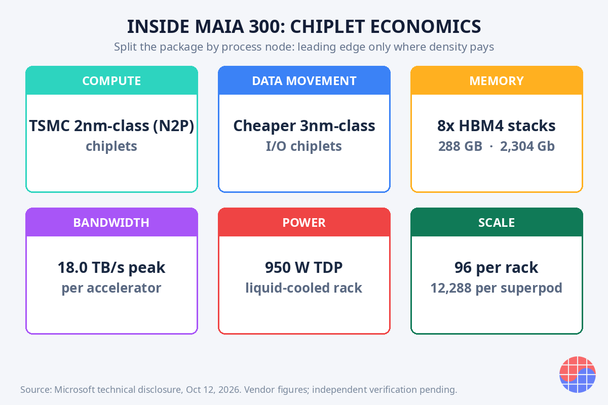
According to Microsoft's technical disclosure (October 12, 2026), Maia 300 is a multi-chiplet package that splits the die by economics, not just by function:
| Block | Detail |
|---|---|
| Compute chiplets | TSMC 2nm-class (N2P) for key computing functions |
| Data-movement chiplets | Cheaper 3nm-class silicon for moving data off the processor |
| Memory | 8 HBM4 stacks, 288 GB (2,304 Gb) per accelerator |
| Memory bandwidth | 18.0 TB/s peak |
| Power | 950 W TDP per accelerator |
| Rack | 96 accelerators, ~167 kW, 27.6 TB of HBM per rack |
| Rack bandwidth | ~1.7 PB/s aggregate memory bandwidth |
| Scale-up | Two-tier Ethernet fabric, up to 128 racks = 12,288 accelerators per superpod |
Three numbers deserve a second look. 288 GB of HBM4 per chip is 2,304 Gb — at more than a million chips, Microsoft is signaling demand for over 8 million HBM4 stacks, or roughly 288 petabytes of HBM4, from the 2027 deployment alone. 950 watts per accelerator puts Maia 300 in the same thermal class as flagship merchant GPUs, which means the same liquid-cooling and power-delivery supply chains. And 96 accelerators per rack at 167 kW doubles the accelerator density of Maia 200 — the unit of competition is no longer the chip, it is the rack.
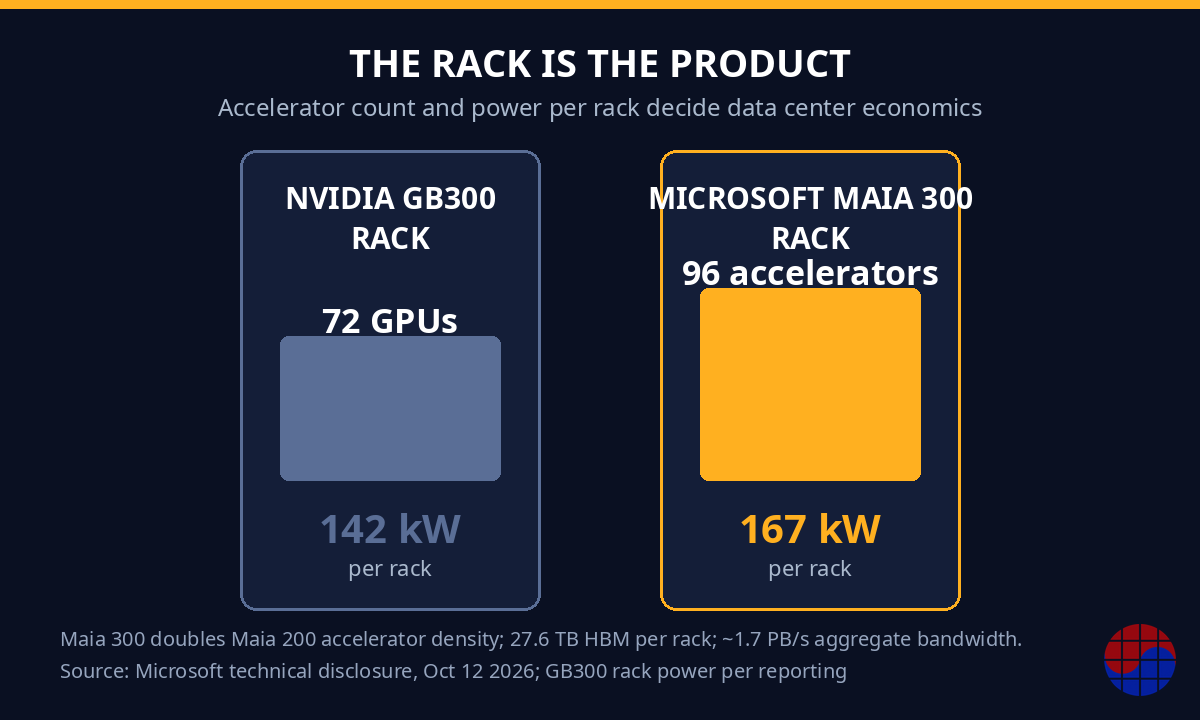
The scale-up fabric is the quiet tell. Maia 300 uses a two-tier Ethernet fabric — electrical links inside the rack, optical links between racks — joining up to 128 racks into a 12,288-accelerator superpod, with bandwidth that job schedulers can reallocate and hot-spare capacity borrowed from neighboring racks. That is a direct architectural bet against proprietary scale-up interconnects: Ethernet, the commodity standard, versus NVLink-style walled gardens. For Broadcom, Marvell, and the Ethernet ecosystem, this is the most consequential design win of the year.
Why inference, why now: the token-economics logic
Training gets the headlines; inference pays the bills. Every Copilot query, every agent loop, every long-context reasoning session is an inference workload billed against Microsoft's own cost structure. As model serving costs fall — intelligence getting cheaper per token — the money pools at whoever serves tokens most cheaply at scale.
That is exactly what Maia 300 is optimized for: 40% more tokens per megawatt and new sub-3-bit and enhanced MXFP4 data formats that squeeze more useful work out of each watt. Microsoft is not trying to beat NVIDIA at peak FLOPS. It is trying to win the metric that decides its own P&L: cost per million tokens served, inside data centers it already owns, on workloads it already controls.
This is the MBA logic in one line: when you own both the demand (Copilot, Azure) and the supply (Maia silicon, data centers), vertical integration converts a variable cost — buying someone else's GPUs at someone else's margin — into a fixed-cost asset you depreciate. The 1-million-chip plan is Microsoft amortizing inference.
The engineer's read: chiplets are a yield decision
Strip away the marketing and Maia 300's package is a textbook lesson in advanced-node economics — the kind you learn on a tapeout floor, not in a strategy deck.
Putting compute on TSMC's 2nm-class N2P while keeping memory-controller and I/O functions on a cheaper 3nm-class node is, first and foremost, a yield and cost play. Bleeding-edge nodes are where defect density hurts most and wafer prices bite hardest; you put only the logic that truly needs the density there, and you keep everything else on a mature, high-yielding node. Known-good-die economics then decide the package yield instead of one giant monolithic die deciding it.
Second, the HBM4 interface is the real signoff challenge. Eight stacks at 18.0 TB/s means the PHY, the interposer routing, and the power-integrity work around the memory subsystem dominate the physical design effort — far more than raw logic timing closure. Anyone who has done STA signoff on a large SoC knows the pattern: the headline number is bandwidth, but the tapeout risk lives in the interfaces.
Third, rack-level co-design is the new floorplan. Liquid cooling carrying most of a 167 kW rack's thermal load, 950 W packages, optical inter-rack links — the power-delivery network and the thermal envelope now constrain architecture before the RTL does. The chip team that does not co-design with the rack team ships a part the data center cannot house.
What it means for NVIDIA
The near-term risk to NVIDIA is bounded: Microsoft still buys its GPUs at scale, and training — NVIDIA's stronghold — is untouched by an inference-first chip. But the direction is unmistakable. Every Copilot query that migrates to Maia is inference revenue that no longer flows through NVIDIA's stack: not the GPU, not the HBM attached to it, not the networking.
More structurally, Maia 300 legitimizes the Ethernet scale-up path at the largest scale in the industry. If the two-tier Ethernet fabric delivers at 12,288-accelerator scale, it weakens the argument that only proprietary interconnects can hold a frontier cluster together — and interconnect lock-in is a pillar of NVIDIA's platform moat.
The third-order effect is pricing power. A credible in-house alternative changes every large buyer's negotiation with merchant vendors. Microsoft does not need Maia to beat the best merchant GPU on every workload; it needs Maia to be good enough on Microsoft's workloads to cap what it pays for the rest.
What it means for memory and foundry
Memory: 8 HBM4 stacks per chip at 1M+ chips is 8M+ HBM4 stacks of incremental demand signal for 2027 — for SK hynix, Samsung, and Micron, all racing to qualify HBM4. Note the unit discipline: 288 GB per accelerator is 2,304 Gb, and rack-level math (27.6 TB per rack) is how data center planners actually buy. The HBM4 supply race just got its biggest demand anchor.
Foundry: compute chiplets on TSMC N2P make Microsoft one of the earliest large-scale N2-family customers, alongside the usual mobile and HPC names. Early N2P allocation at this volume is both a technology statement and a capacity negotiation — and it deepens TSMC's lead as the foundry of the AI era.
The in-house silicon club is now crowded. Google has TPUs, AWS has Trainium, Meta has MTIA, and OpenAI is pursuing its own chip effort. Maia 300's 1-million-unit plan is the largest single deployment commitment among them — a signal that vertical silicon has moved from experiment to procurement strategy.
What to watch next
- Independent benchmarks. Microsoft's 40% tokens-per-megawatt claim names no GPU baseline. Watch for third-party measurements with defined power boundaries and real workloads.
- HBM4 supply. Whether Microsoft can secure 8M+ HBM4 stacks for 2027 while memory stays scarce — and which of the three HBM vendors wins the qualification.
- Outside customers. Microsoft says Maia is for its own products and services. If an external customer ever gets access, Maia becomes a merchant competitor, not just a cost play.
- The Ethernet bet. Whether the two-tier scale-up fabric holds at 12,288-accelerator scale — the result will echo through every networking vendor's roadmap.
The bottom line: Maia 300 is not a chip launch. It is a procurement strategy with a die photo. Microsoft looked at the largest line item in its AI P&L — inference compute — and decided to manufacture it. For the semiconductor industry, the message is that the customer is now also the competitor, and the negotiation happens in tokens per megawatt.
FAQ
What is Microsoft Maia 300?
Maia 300 is Microsoft's third-generation in-house AI accelerator, announced on October 12, 2026 and designed for inference workloads such as coding assistance, long-context reasoning, and agentic tasks. It uses a chiplet architecture with compute dies on TSMC 2nm-class silicon, eight HBM4 stacks (288 GB, 18.0 TB/s), in a 950 W envelope, deployed in 96-accelerator racks.
How many Maia 300 chips will Microsoft deploy?
Reuters reported (October 16, 2026) that Microsoft plans to deploy potentially more than one million Maia chips in 2027, scaling the Maia family to multi-gigawatt deployments as the primary inference system for its own products and services. Production deployments begin in 2027.
How does Maia 300 compare to NVIDIA's GPUs?
Microsoft claims about 40% more tokens per megawatt than unnamed "leading GPU-based systems" and up to 7x the rack-level token throughput of its predecessor Maia 200 — both vendor claims awaiting independent verification. Architecturally, Maia 300 bets on a two-tier Ethernet scale-up fabric versus proprietary interconnects, and targets inference cost efficiency rather than peak training FLOPS.
What does Maia 300 mean for HBM and foundry suppliers?
At 8 HBM4 stacks per chip and 1M+ chips planned, the 2027 deployment implies demand for 8M+ HBM4 stacks (~288 petabytes) — a major demand anchor for SK hynix, Samsung, and Micron's HBM4 ramps. The compute chiplets on TSMC's N2P node also make Microsoft an early large-scale customer for TSMC's 2nm-class capacity.
Disclosure: This analysis is based on Microsoft's October 12, 2026 announcement and subsequent reporting (Reuters, October 16, 2026); performance figures are Microsoft's claims and have not been independently verified. The author holds no position in the companies discussed. Figures reflect disclosures as of October 17, 2026.