VLSI Korea
Why NAND uses two wafers: CBA's thermal freedom and bonding yield
Separating the memory array from its peripheral circuitry creates process freedom. Whether that freedom lowers cost depends on how many good bits survive bonding.


The race to add NAND layers also contains a different architectural change: build the storage cells and their CMOS peripheral circuits on separate wafers, then join them. Kioxia's CMOS directly Bonded to Array, or CBA, is one example.
The economic question is straightforward. Why pay for another wafer and an additional bonding process? The answer lies in the thermal constraints imposed by a shared manufacturing flow and the yield cost introduced by separating it.
For a process engineer, the practical decision is which loss mechanism and measurement to prioritize. For an SSD designer, it is how to connect a NAND interface improvement to system requirements. Public process descriptions and explicitly illustrative calculations help separate those decisions.
| Change | Resource affected | What it does not establish |
|---|---|---|
| Separate array and CMOS | Pre-bond process freedom | Final good-bit cost |
| Finer bonding pitch | Interconnect placement density | SSD throughput |
| Better bond survival | Functional output | Equal workload performance |
VLSI Korea view: Evaluate CBA through good bits obtained per unit of process cost, rather than through layer count or bonding pitch alone.
Read the manufacturing question behind the partnership
On 2026-09-29, Applied Materials announced that Kioxia would join its EPIC Center as a research partner. The collaboration covers memory structures, multi-chip stacking, packaging and materials engineering. It describes a development agenda, rather than production volumes or yield for a particular memory generation. Official announcement
The useful signal is that memory improvement extends beyond shrinking cells. Conditions that favor the array, those that favor peripheral circuits, and those that favor their interconnection must work together. A tool's best isolated result matters less than a process window that remains compatible with the surrounding steps.
CBA did not originate with this partnership. In its 2024-03-14 technical explanation, Kioxia described separate CMOS and array wafers connected through direct copper bonding. The same account identifies the underlying work as a presentation at IEDM in 2023. The new collaboration creates a reason to revisit how this established approach might extend to future memory structures. Technology account
A shared wafer also shares a thermal history
The array stores and distinguishes charge. Peripheral CMOS selects addresses, senses signals and moves data out. These functions differ, so their preferred manufacturing conditions need not coincide.
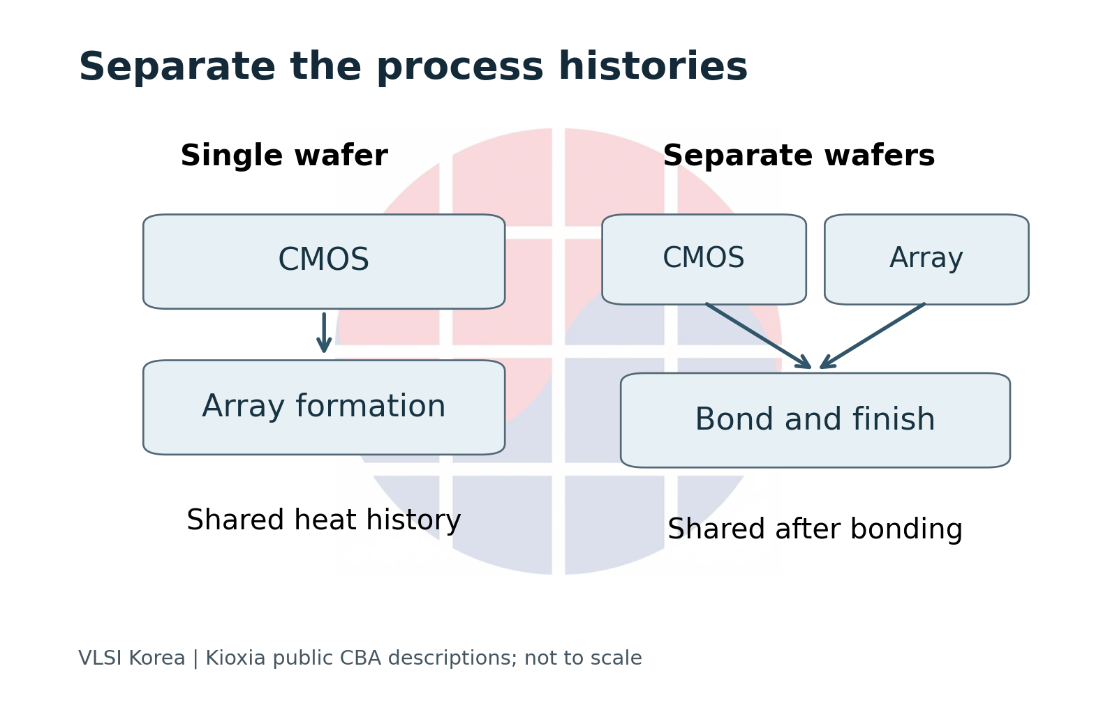
With CMOS Under Array, or CUA, array formation follows CMOS fabrication on the same wafer. The existing CMOS therefore experiences heat from subsequent array processing. CBA separates the fabrication flows before joining them. Kioxia identifies the ability to optimize their thermal processes separately as a benefit. Structure comparison
Consider this as a process-sequencing problem. Adding a thermal treatment to a shared wafer requires more than showing that the cells benefit. The devices and wiring already underneath must also tolerate it. Separate flows allow teams to explore conditions before bonding without subjecting the other wafer's circuitry to the same treatment.
Separation does not eliminate every thermal constraint. Once the wafers meet, they share downstream processing. The completed stack must tolerate bond-strengthening anneals, subsequent thinning and interconnection work. The precise benefit is therefore a wider choice of processing conditions before bonding.
| Manufacturing flow | Before integration | After integration |
|---|---|---|
| CMOS Under Array | Sequential processing on one wafer | Shared thermal history |
| CMOS directly Bonded to Array | Array and CMOS formed separately | Shared downstream limits |
This distinction also matters when comparing products. An improvement in cell current, interface speed or energy consumption creates a different kind of design headroom. Before valuing a structural change, identify the constraint to be relaxed. Increasing affordable capacity and improving a read path are different objectives, even when the same process technology contributes to both.
Bonding has separate height and alignment problems
Placing wafers together does not automatically establish electrical continuity. The relative height of the dielectric surface and copper pads must be suitable, and opposing pads must be aligned. The first is a surface-topography problem; the second is a positioning problem.
Kioxia describes chemical mechanical polishing, or CMP, to control the pad-to-dielectric step height, followed by wafer alignment, contact and annealing to establish the copper connection. Residual gaps between pads can prevent the required electrical contact. CBA process
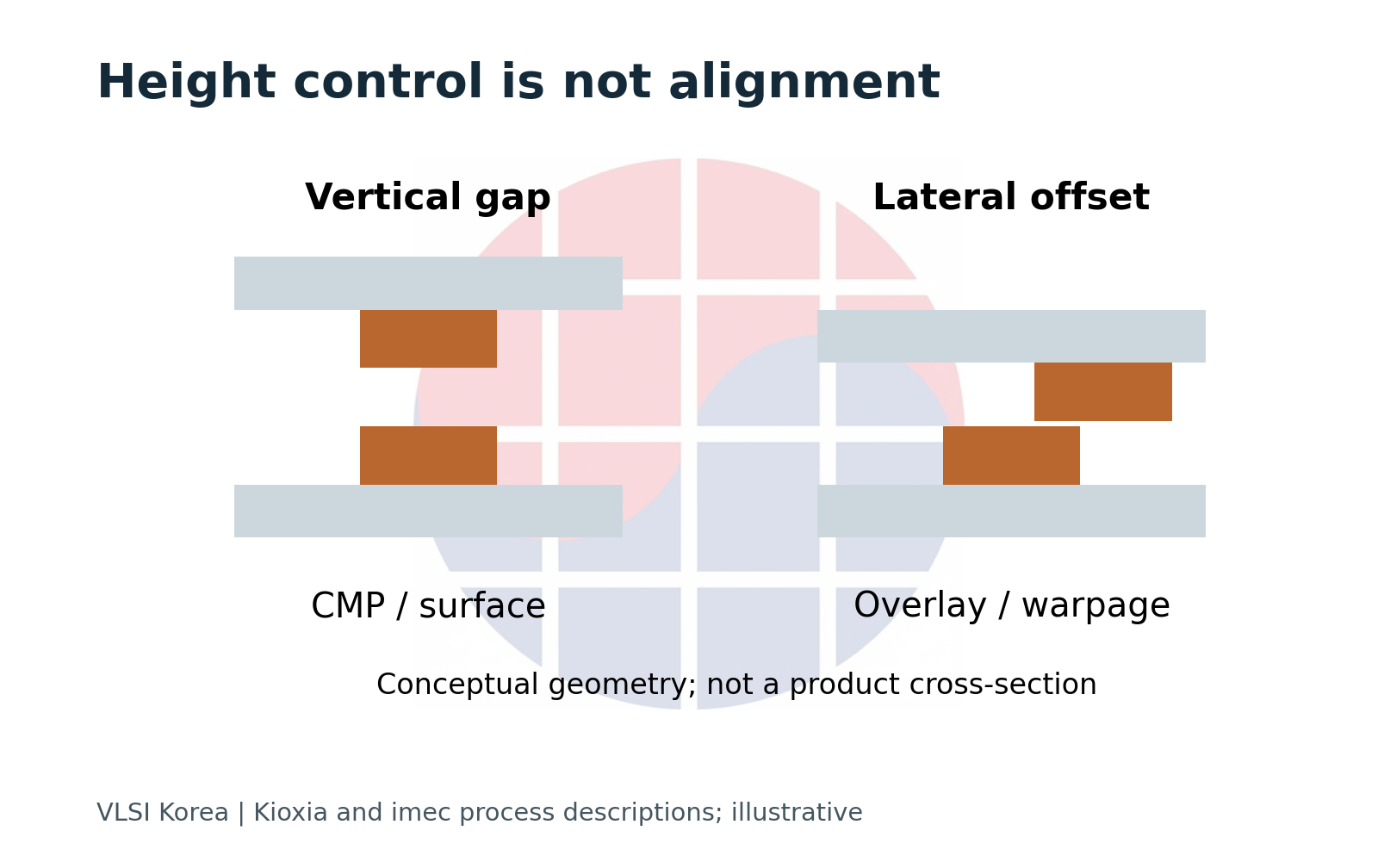
A perfectly flat surface can still be misaligned. Accurate centering can still leave a surface-height problem. A diagnosis based only on a bonder's alignment specification is therefore incomplete. Relating electrical failures to surface topography and wafer deformation gives a more useful picture.
Imec's 2024-02-19 account also examines CMP, cleanliness, pad design and alignment together. Its 400 nm pitch work treats connection reliability as a separate concern. This is evidence of shared integration challenges, rather than a process specification for a Kioxia product. Imec research account
Bonding pitch should not be confused with NAND cell size or layer count. It describes spacing between inter-tier connections, while layer count describes repetition within the vertical array. The numbers refer to different resources, even when both appear in the same scaling discussion.
Good bits must repay the additional wafer cost
A smaller die can provide more candidate sites on a wafer. But paying for both wafer flows and bonding means that site count alone cannot establish the economics. The denominator must include the amount of functional memory that remains.
| Pairing mode | Selection freedom | Cost-model implication |
|---|---|---|
| Wafer to wafer | Corresponding sites meet | Defect-map overlap matters |
| Die to wafer | Individual dies can be selected | Add screening and placement costs |
Even before multiplying yields, establish how sites are paired. In wafer-to-wafer bonding, a good site on one wafer can face a bad site on the other. High individual wafer yields do not mean every good die can be combined with a freely chosen good counterpart.
Consider a deliberately simplified design example. Let a baseline batch cost 100 and produce 900 good dies of equal capacity. Its cost per good capacity unit is 100 ÷ 900. These are arbitrary cost units, not a manufacturer's costs or a currency estimate.
For the bonded flow, assume an array-wafer cost of 55, a CMOS-wafer cost of 45 and bonding cost of 15, for a total of 115. Assume layout and area improvements provide 1,250 paired sites of the same capacity. With array yield of 95%, CMOS yield of 96% and bonding survival of 99%, expected good output is:
1,250 × 0.95 × 0.96 × 0.99 = 1,128.6
The fractional result is an expectation across repeated batches. Assume independent defect locations across the two wafers and bonding survival conditional on both circuits being good. Cost per good capacity unit becomes 115 ÷ 1,128.6, approximately 8.3% below the baseline.
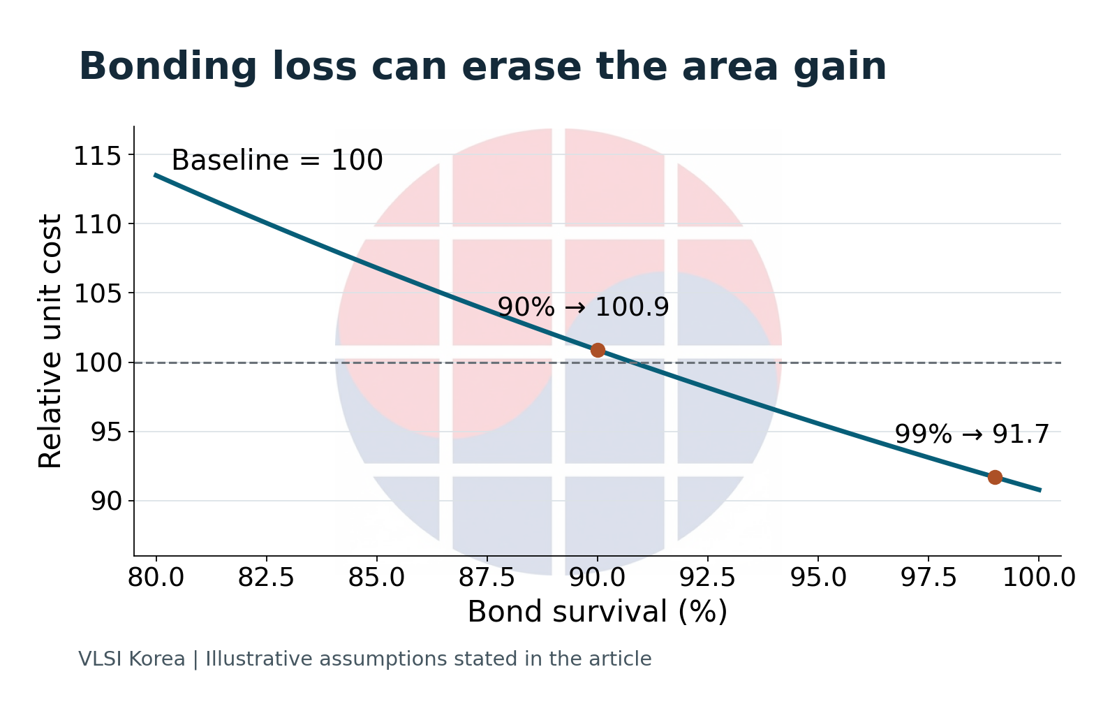
Reduce only bonding survival to 90% and good output becomes 1,026. Unit cost is then approximately 0.9% above the baseline. Holding the other assumptions constant, break-even bonding survival is approximately 90.8%. Bonding losses can consume an otherwise useful area advantage.
The general expression is C ÷ (N × Y_array × Y_CMOS × Y_bond × B). C is total process cost within the comparison boundary, N is the number of paired sites, each Y is the relevant survival fraction, and B is capacity per good die. The example holds B equal between alternatives, allowing it to cancel.
C also needs the same accounting boundary on both sides. Including bonding and testing in one flow while counting only fabrication in the other mixes architectural differences with accounting differences. Define the boundary from batch input to output passing the same functional test, then replace illustrative assumptions with recorded values within that boundary.
| Quantity | Meaning in this model | Comparison requirement |
|---|---|---|
| Total cost C | Costs inside the selected boundary | Same accounting boundary |
| Good capacity | Functional output after bonding | Same capacity definition |
| Product value | Performance and endurance at workload | Evaluate separately from cost |
This separates cost from performance. If a larger die capacity changes write behavior, an increase in B alone does not establish equivalent product value. Compare capacity that meets the same workload performance and endurance requirements. If additional channels or packages are needed to recover performance, system cost changes again.
The example is a simple wafer-to-wafer model. Correlated defect maps, unequal die capacities, repairable defects and testing costs require a different formulation. Die-to-wafer placement of screened dies needs a different model.
Design decision: Do not approve a cost-reduction claim using throughput and alignment precision alone. Connect area gain, the good-site distributions on both wafers and final good capacity within the same batch boundary.
Many connections amplify losses hidden by an average
Bonding success needs a denominator: a pad, a complete daisy chain or a memory die meeting its specification.
Take an intentionally extreme simplification. If 1,000,000 connections are essential and each independently fails with probability p, the probability that all work is (1-p) raised to 1,000,000. At p = 0.00000001, the result is approximately 99.0%; at p = 0.0000001, it is approximately 90.5%. A small change in individual failure probability creates a substantial change in the aggregate.
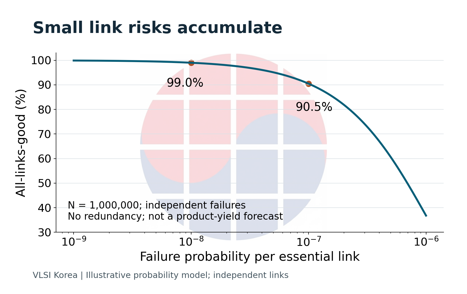
Real memory does not treat every connection this way. Spare resources or defect bypass may exist, while a particle or local deformation can affect multiple connections together. The calculation explains why an excellent average contact result cannot substitute for die yield; it does not forecast a product's yield.
Transferring a test structure into a product requires examining both connection count and failure tolerance. A simple chain can reveal broken contacts without representing a memory's spare resources or operating conditions. Conversely, a functional pass alone does not characterize long-term thermal history. Different measurements answer different questions.
Useful shared evidence therefore extends beyond average contact resistance. Resistance distributions, open and short locations, changes after thermal processing and final functional results should be connected through common coordinates and process histories. That is what makes the decision about the next process improvement specific.
Interconnect density and SSD performance live at different levels
On 2026-05-28, imec and EV Group announced a wafer-to-wafer hybrid-bonding test vehicle with 200 nm pitch in connection with ECTC. This is an interconnect research result, not evidence that Kioxia NAND uses the same pitch. Official announcement

Smaller spacing creates room for more potential connections within a fixed area. Making those connections useful also requires circuitry, power and routing resources. Halving bonding pitch therefore does not imply the same proportional improvement in memory speed or SSD throughput.
Product specifications also have boundaries. Kioxia's 2024-07-03 QLC sample announcement specified a 3.6 Gbps interface and identified a particular test environment. That is a different metric from sustained writes on a complete SSD. Contemporaneous product announcement
An SSD designer should first ask which waiting time the interface improvement could reduce. Is the workload waiting for array data, channel transfer, the controller or the host path? The answer changes where resources should go. Additional interface headroom leaves user-visible throughput constrained if another stage remains the bottleneck.
For Korean suppliers, the question is which yield they improve
Korean memory, equipment and materials teams can evaluate this trend by defining the loss mechanism their process changes. CMP materials connect to surface topography; cleaning connects to pre-bond surface condition; metrology helps distinguish causes and locations. These are implications of the process flow, not forecasts of orders for particular companies.
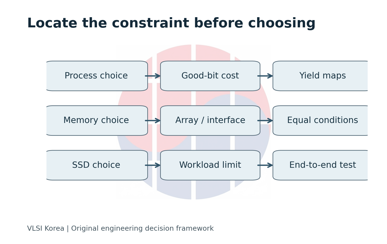
The process team's decision is whether the current bottleneck is reproducing a promising performance result or stabilizing the distribution of good output. The design team's decision is whether to use additional cell or interface headroom for throughput, power or capacity configurations. Those teams need different evidence from the same technology announcement.
The same framework can guide reading over the next 6-12 months. Separate progress in test structures from functional memory, compare good-bit cost at equal capacity and conditions, and ask whether interface improvement relaxes the actual workload constraint. Combining results from different products and conditions destroys the comparison.
CBA pays for another wafer to separate manufacturing flows. That choice can allow the array and CMOS to be built under individually favorable conditions. The final economic test is whether enough good bits remain after the two wafers are joined.
Sources
- Applied Materials: Kioxia joins the EPIC Center, 2026-09-29
- Kioxia: CBA technology development, 2024-03-14
- Kioxia: CBA structure and process explanation
- imec: 400 nm wafer-to-wafer bonding, 2024-02-19
- imec and EV Group: 200 nm bonding test vehicle, 2026-05-28
- Kioxia: QLC sample announcement, 2024-07-03
Disclosure
This article is provided for informational purposes only and does not constitute a recommendation to buy or sell any security. Figures and factual statements are based on publicly available sources, including company filings, news reports, and market research, and may contain errors in the source material or in the preparation of this article. The author may own shares in companies mentioned. All investment decisions and their outcomes are the reader's responsibility.