VLSI Korea
Why Quad SPI Does Not Automatically Make a Sensor Faster
Starting with new TinyProbe research, calculate the effects of burst length, controller limits, buffering and wireless delivery before adding data pins.


Adding SPI data lanes increases the number of bits moved during the payload phase. It does not guarantee a proportional increase in the rate of complete frames reaching the user.
Command time, the selected controller's clock, buffer occupancy and overlap with the next transfer stage matter together. Before redesigning a board, calculate which reduction in waiting time would make complete data arrive more often.
| Boundary | Keep fixed | Record |
|---|---|---|
| Pins | Board, voltage, lane mode, clock | Pattern errors, timing conditions |
| Transaction | Payload length, command format, gaps | Useful bytes and elapsed time |
| Host delivery | Acquisition setting, network load | Complete frames, loss and latency |
Table 1. Editorial test framework, not a claim that these tests were performed here.
A TinyProbe multi-wire SPI preprint submitted on 2026-10-01 makes the question concrete. Its authors report Dual SPI validation at 5 MHz in an integrated IGLOO2/SiWG917 configuration, and Quad SPI tests up to 66 MHz on a separate Kria K26/STM32N6 testbed.
The latter corresponds to a raw payload-phase rate of 264 Mbit/s, not the wireless throughput of the complete probe. Full paper
VLSI Korea view: Judge a wider bus by how much it reduces the system's limiting wait, rather than by its maximum bit rate alone.
This article helps FPGA engineers choose bus width and burst length, and system owners choose between firmware work and controller replacement. The calculations are reusable design examples into which readers can insert their measurements, rather than benchmarks of a particular product.
The same bits cross different measurement boundaries
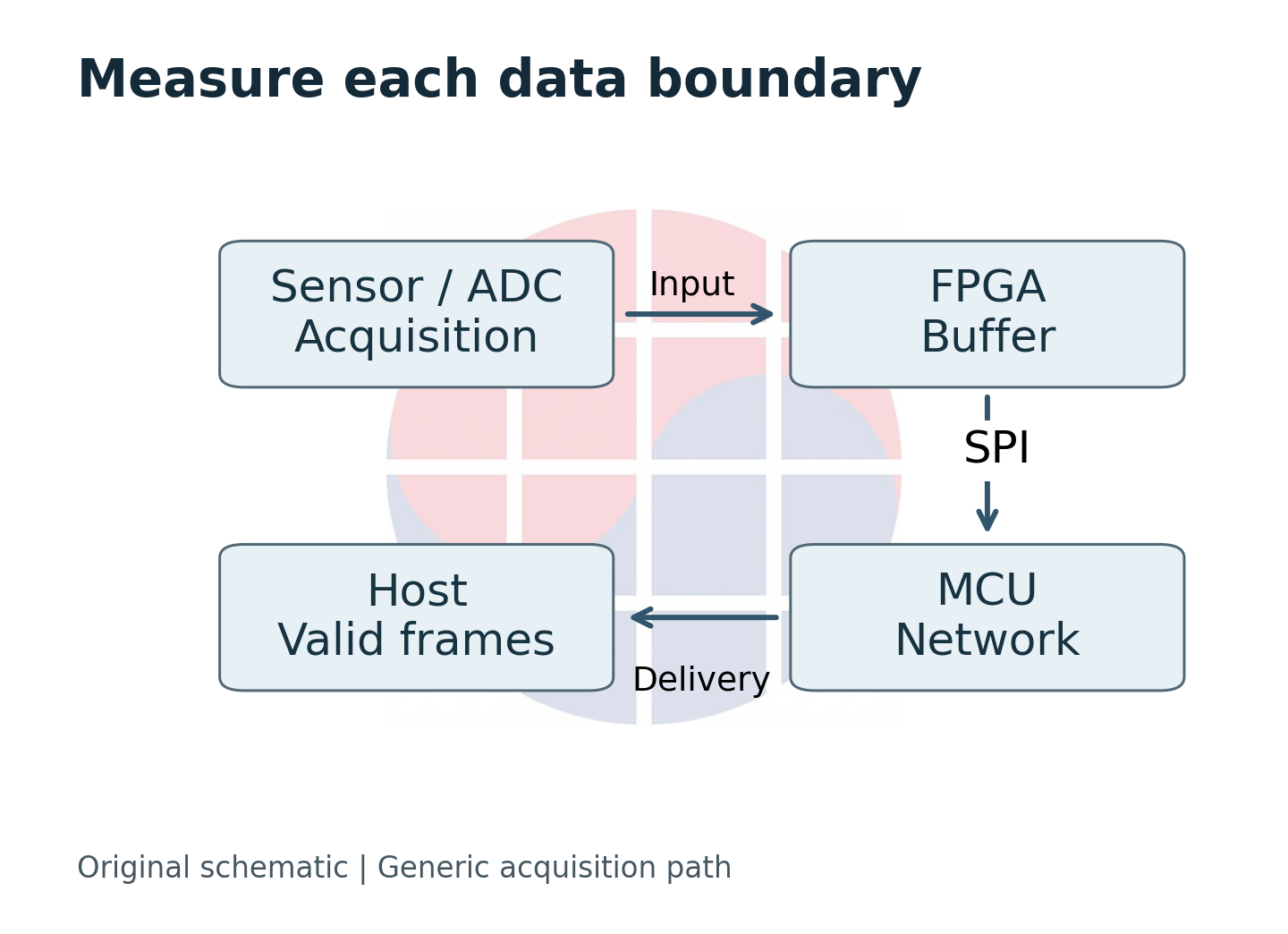
Separate the sensor path into data generation, temporary storage, on-board transfer and network delivery. Each boundary gives speed a different denominator.
ADC sampling describes the ability to convert inputs into numbers; SPI bit rate describes movement over particular wires. Host throughput counts the data that actually arrives and is accepted as useful.
A larger upstream number does not establish a larger downstream result.
TI's AFE5832LP product information describes 32 input channels and an LVDS output, the boundary between analog reception and digital acquisition.
Dividing a sample-rate specification from that page by the downstream MCU's SPI rate would omit channel selection, acquisition duration, storage format and transfer intervals. Component maxima and operating conditions must remain distinct. TI product information
Begin by fixing the throughput definition. Will it count acquired raw samples, buffers without headers, or complete frames assembled at the host?
Then measure time with the same start and stop conditions. Counting retransmitted bytes as additional output, or treating a send function's return as host arrival, produces incompatible performance tables for the same system.
Agree on that before choosing instruments.
More lanes require checking clocks and direction
A conventional single-data-line SDR transfer moves a bit in the relevant direction per clock cycle. Dual and Quad modes use additional lines in parallel during the payload phase.
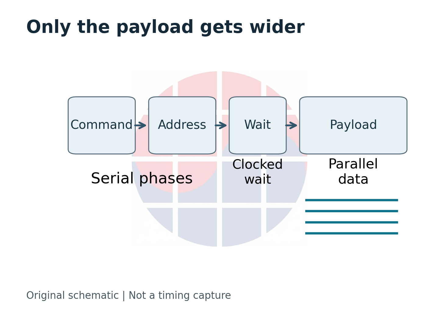
Whether commands and addresses also use that width is a separate condition. Silicon Labs' SSI architecture guide distinguishes instruction, address, wait and data phases, with configurable transfer formats.
A “Quad supported” label therefore does not establish that every part of a transaction becomes wider. SSI architecture
Another trap is assuming identical clock limits across modes. The 917 developer guide v1.0.3 FAQ states up to 40 MHz for standard SPI and up to 10 MHz for Dual/Quad.
Yet the architecture chapter in the same version includes a DMA-dependent Quad calculation yielding 22.5 MHz. The documentation does not resolve into a single unconditional ceiling.
The device, SDK and pin configuration need to be checked together; the FAQ values are not treated here as universal measured limits. FAQ
Review who drives each signal in each phase, rather than relying on its name. A line used as an output in single SPI can become an input during a multi-line read.
Simultaneous driving at both ends creates electrical contention; switching direction too late can lose the first data. Wait cycles, sampling edges and chip-select behavior must agree at both ends.
Copying the maximum shown in a configuration menu does not establish compatibility. SSI configuration guide
In a short transfer, the command can cost more than the data
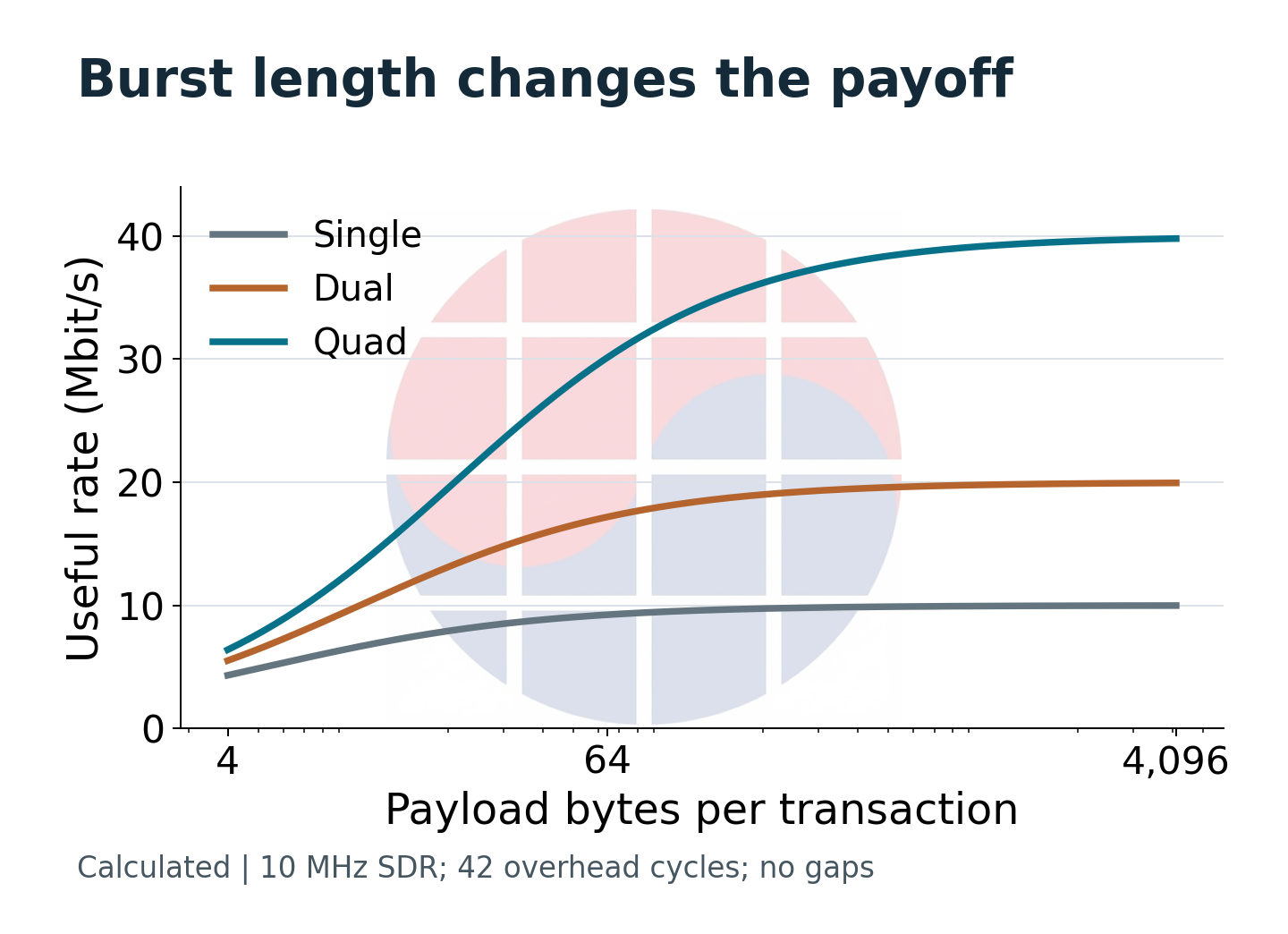
To isolate the effect of width, define an illustrative read. Every mode uses a 10 MHz clock, an 8-bit instruction on a single line, a 24-bit address on a single line, and 10 wait cycles.
Only the payload width changes with the number of lanes L. These are common comparison assumptions, not a guarantee that a particular MCU supports every combination.
Initially exclude chip-select gaps and software delays.
A transaction carrying N bytes requires 42 + 8N/L clock cycles. Its useful payload rate is therefore 8N × f / (42 + 8N/L), where f is the clock frequency per second.
Keeping bits in the numerator and time in the denominator also avoids confusing MHz with Mbit/s. The raw rate L × f is approached when the payload phase dominates the transaction.
For a 4-byte read, single-line operation delivers about 4.32 Mbit/s, Dual 5.52 Mbit/s and Quad 6.40 Mbit/s. Additional lanes do not remove the instruction, address and wait time already paid.
By contrast, a Quad transaction carrying 4,096 bytes reaches about 39.80 Mbit/s, close to the raw rate of 40 Mbit/s. This explains why the same Quad mode looks so different when reading a small register and a large sample buffer.
| Payload per transaction | Single, Mbit/s | Dual, Mbit/s | Quad, Mbit/s |
|---|---|---|---|
| 4 bytes | 4.32 | 5.52 | 6.40 |
| 64 bytes | 9.24 | 17.18 | 30.12 |
| 4,096 bytes | 9.99 | 19.95 | 39.80 |
Table 2. The same illustrative assumptions as Figure 3; values rounded to 2 decimal places.
Ever-longer bursts are not a universal solution. They occupy receive buffers longer and can extend other work's waiting time.
An error during a long transaction can also enlarge the unit that must be retransmitted. Splitting the payload can be preferable when control commands have tight response deadlines.
Establish the acceptable delay first, then choose a burst large enough to dilute fixed overhead within that limit.
A FIFO does not eliminate an average-rate imbalance
A buffer lets a producer and consumer work at different moments. But if average input exceeds average output, a finite buffer eventually fills.
Distinguish this capacity problem from clock-domain crossing, or CDC, correctness. A safe crossing can still have insufficient capacity; abundant capacity cannot compensate for incorrectly transferred status signals.
AMD's Embedded FIFO Generator PG327 requires write and read interface signals to be used in their respective clock domains and requires respecting full and empty status. Independent-clock FIFOs also introduce synchronization delay when these flags deassert.
Freeing space does not make that space immediately visible at the other interface. This is a description of that IP, not a claim that TinyProbe uses it. Synchronization guidance, flag behavior
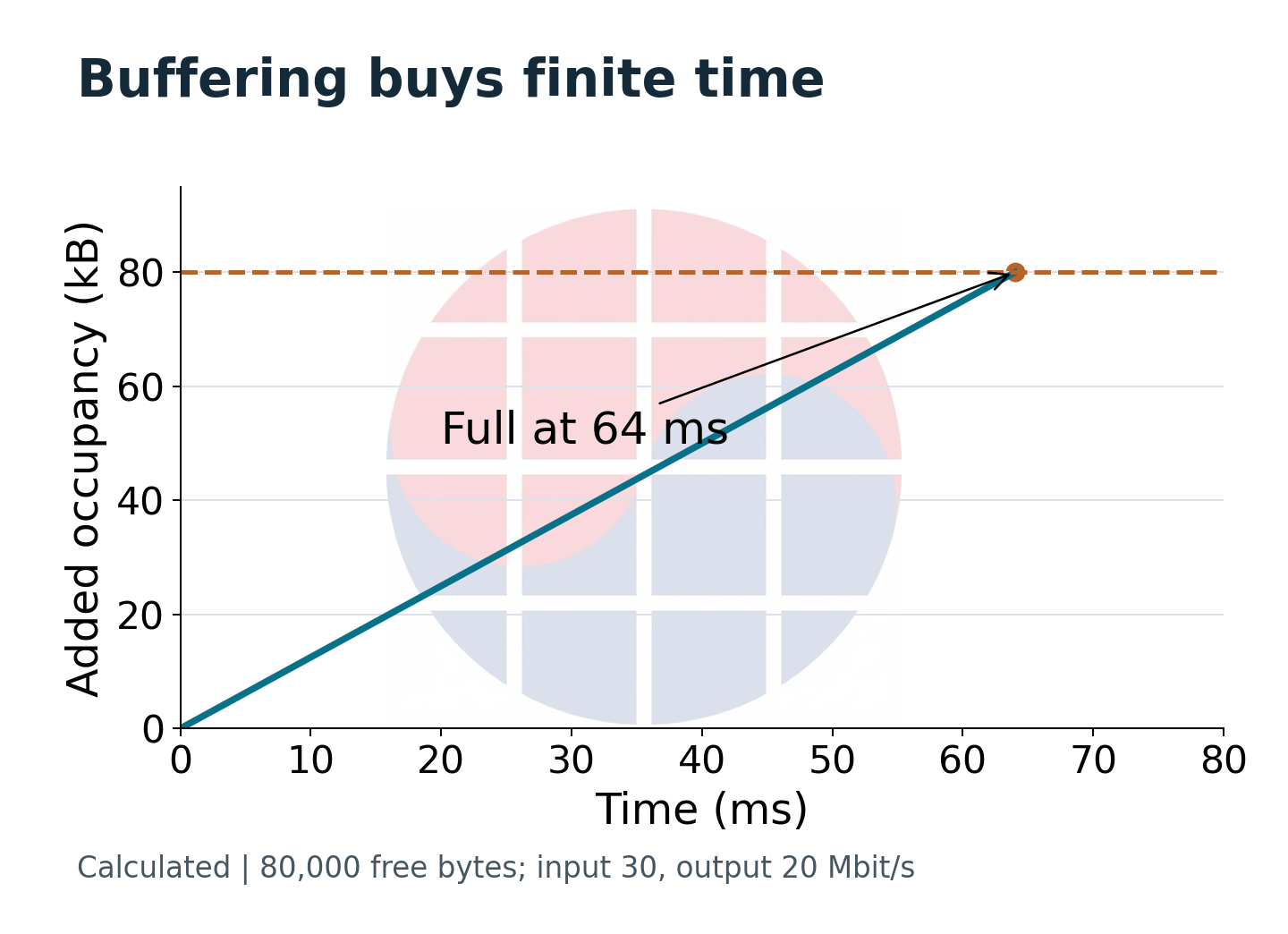
In the illustrated example, 80,000 free bytes hold 640,000 bits. Dividing by the difference between 30 Mbit/s input and 20 Mbit/s output gives 64 ms before the free space disappears.
Existing occupancy or a pause in DMA service shortens that time. The design therefore needs more than a depth value: it needs a worst-case service interruption, an acceptable loss policy and a statement of whether the producer can stop.
When acquisition cannot stop, additional buffering buys time rather than sustained throughput.
Data units matter too. Differences between sample width and memory storage width introduce padding or repacking.
Converting transferred bytes into useful sensor bits must account for that ratio. DMA does not necessarily remove memory copies, cache management or completion handling.
Measuring SPI while excluding those costs makes firmware changes difficult to compare fairly.
Overlap with wireless delivery changes the result
Once the board's SPI link becomes faster, examine the path from MCU to host. Even the familiar claim that the slowest link determines system speed has a condition.
In steady state, when stages handle different data batches simultaneously, the slowest stage sets an upper bound. If the system instead reads a complete buffer before starting its network transfer, and pauses the next read meanwhile, the stage times add.
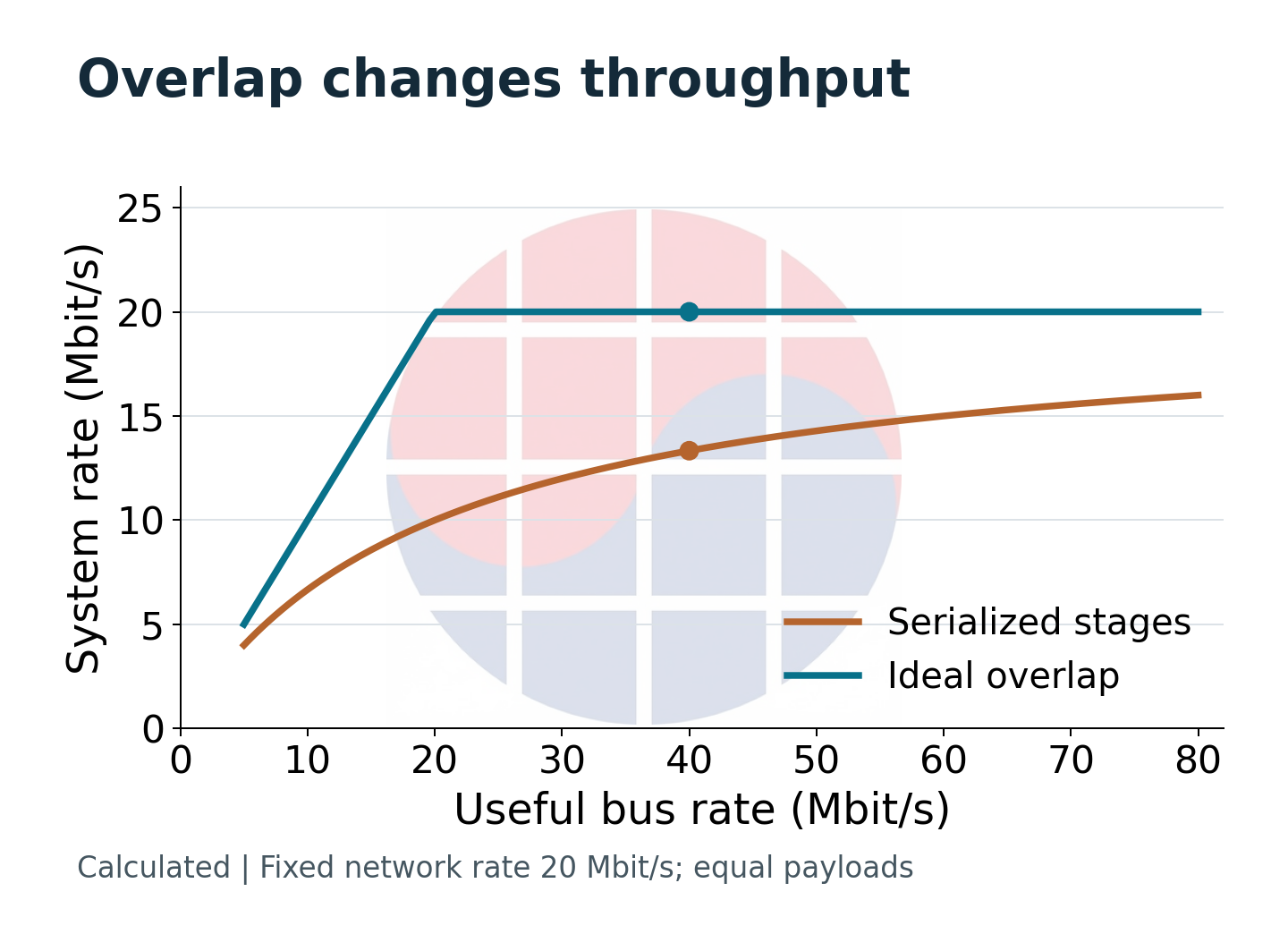
Suppose the bus moves useful payload at 40 Mbit/s and the network moves an equal payload at 20 Mbit/s. Fully serialized stages yield 1 / (1/40 + 1/20), or about 13.33 Mbit/s.
With sufficient independent buffers and resources to overlap stages, the ideal steady-state ceiling is 20 Mbit/s. These are separate illustrative assumptions, not TinyProbe measurements; protocol costs and acquisition time are excluded.
| Scheduling | Model denominator | Limiting condition |
|---|---|---|
| Serialized | Sum of stage times | Each batch waits for the next stage |
| Overlapped | Slowest stage in steady state | Independent resources and buffers |
Table 3. Original model comparison. First-frame latency still includes every required stage.
This distinction changes the intervention. If transfers cannot overlap, changing buffer ownership and DMA completion handling can be more useful than adding pins.
If stages already overlap sufficiently and the network is saturated, additional on-board bandwidth may create timing margin or reduce part of the latency without increasing frame rate. The product value of the same optimization depends on its starting conditions.
Boundary condition: A pipeline throughput ceiling is not a first-frame arrival time. Overlap does not remove the stages that each frame must traverse.
Not every wireless gap comes from radio conditions. MCU copies, shared-memory access and packet batching can make the bus and network alternate between work and waiting.
Connecting timestamps for data generation, read completion, send handoff and host reassembly reveals whether the product needs a faster radio or less waiting between existing resources.
Moving from a successful testbed to a product specification
Separate the TinyProbe tests: the isolated testbed explores interface range; integration checks the connected configuration.
Different FPGAs and controllers do not establish a system speedup factor. No observed errors is not an error-rate guarantee across temperature, voltage and wiring conditions.
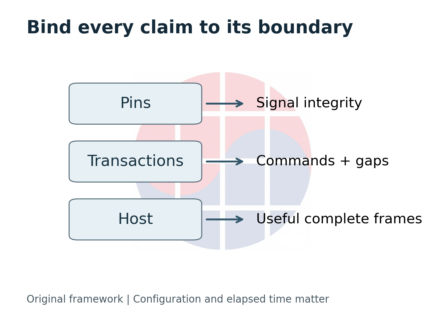
A design-review performance table should preserve the payload phase at the pins, the transaction including commands and gaps, and complete useful data at the host. Connecting these boundaries explains both bus improvements and system improvements.
A faster bus with an unchanged host result is still an informative observation about the bottleneck.
Start with repeating patterns to check wiring and bit order, then add real sample formats and buffer boundaries. Finally, introduce network load and service gaps to observe what is lost during overflow and how recovery works.
Fix the comparison variable and hold other conditions constant; changing everything at once prevents attribution. Selecting only successful short transfers can hide weaknesses in prolonged acquisition.
For Korean design teams, change the denominator first
For Korean sensor-module, FPGA and embedded-product teams, this is also a component-selection and scheduling problem. A wider interface brings pins, routing, drivers and validation work.
Replacing a controller can affect power states and software assets. Conversely, a bottleneck resolved through burst aggregation or transfer overlap can extend the value of an existing board.
Purchase price alone does not determine the cheaper path.
| Observed constraint | Candidate intervention | Tradeoff |
|---|---|---|
| Short transactions | Aggregate bursts | Control latency and buffer occupancy |
| Stages take turns | Overlap transfers | Buffer ownership and memory contention |
| Bus stays saturated | Wider or faster interface | Pins, power and validation effort |
Table 4. Editorial decision framework. Choose the intervention only after measuring the stated constraint.
The numbers engineering sends to procurement and product management should therefore describe when the required data arrives and which configuration achieves it, rather than only a maximum clock. Ask which wait the change removed and whether more complete frames arrive under the same input and loss conditions.
The case for a component replacement rests on completing useful work with less delay or fewer resources.
Over the next 6–12 months, the useful observation is integrated-path evidence rather than another high-clock demonstration. Follow-up TinyProbe material identifying controller and firmware versions and connecting buffer policy to useful host throughput would make the product value easier to judge.
The next editorial reassessment date is 2027-04-03. It is not a product-release forecast.
The condition that would change this article's judgment is explicit. If, with identical input, network and power conditions, the current bus remains saturated and the host still waits despite sufficient overlap, widening the bus becomes a direct priority.
Until then, define the boundaries and measure the time spent in each before choosing the lane count. Good interface design explains what the larger number removes from the reader's system.
Sources
- TinyProbe multi-wire SPI paper, arXiv v1. Full preprint read. The IUS 2026 acceptance statement in the submission record is author supplied; final IEEE publication was not independently confirmed.
- Silicon Labs SSI developer guide v1.0.3, FAQ, configuration. These belong to the same manufacturer's documentation set.
- TI AFE5832LP product documentation. Public product page inspected.
- AMD PG327 synchronization and flags, version 1.0, 2023-05-16.
- TinyProbe official repository, photo authorship, image license. The actual TinyProbe photograph is by Sergei Vostrikov and used under CC BY 4.0. It does not establish that the board shown contains the paper's new interface.
Calculations and diagrams are explanatory VLSI Korea models, not evidence of experiments performed here. AI assisted preparation of the text, translation and explanatory material.
Disclosure
This article is provided for informational purposes only and does not constitute a recommendation to buy or sell any security. Figures and factual statements are based on publicly available sources, including company filings, news reports, and market research, and may contain errors in the source material or in the preparation of this article. The author may own shares in companies mentioned. All investment decisions and their outcomes are the reader's responsibility.