VLSI Korea
The RTL-First Full-Stack Chip Roadmap: Learn in Tapeout Order
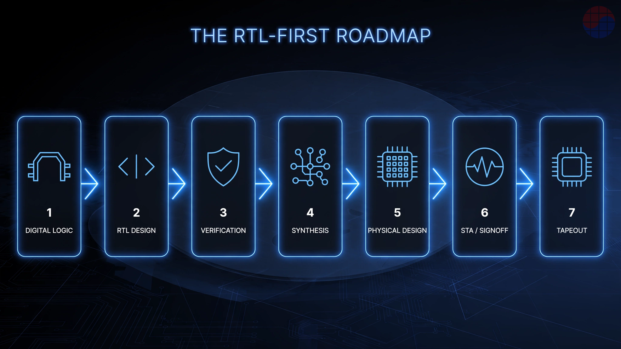
30-Second Summary * Learn chip design in tapeout order. Digital logic → RTL design → Verification → Synthesis → Physical design → STA/signoff → Tapeout. That order is the whole thesis. * Why RTL first: every later stage (verification, PD, STA) is the job of reading and judging the output of the earlier stage. If you can't read RTL, waveforms, timing reports, and congestion


30-Second Summary
- Learn chip design in tapeout order. Digital logic → RTL design → Verification → Synthesis → Physical design → STA/signoff → Tapeout. That order is the whole thesis.
- Why RTL first: every later stage (verification, PD, STA) is the job of reading and judging the output of the earlier stage. If you can't read RTL, waveforms, timing reports, and congestion maps are all half-legible.
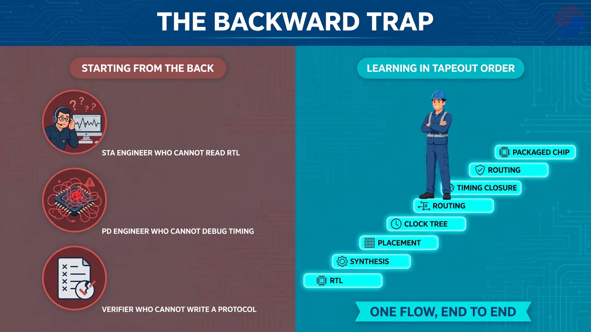
- Starting from the back produces engineers who know their stage but not the chip. They can read an STA report but can't find the RTL bug behind it; they can run a PD flow but can't diagnose a timing violation's root cause.
- You can run all 7 stages at home with open-source tools only. Icarus Verilog/Verilator → Yosys → OpenROAD/OpenLane → OpenSTA → Magic/KLayout + the Sky130 PDK. OpenROAD has been used in 600+ real tapeouts through the Efabless MPW shuttle program.
- One full pass takes 12–18 months of self-study. One working project per stage is the bar. Skip nothing.
Intro: Why Order Is Skill
The most common question from aspiring chip designers is: "Should I start with verification or physical design?" Bootcamps tell you to pick one. Forums say "STA pays well."
Here's the honest answer. What matters more than where you start is whether you skip what comes before. Chip design is a pipeline. Each stage's output is the next stage's input. Learn it backwards and you end up in a strange state: fluent with the tools of your stage, illiterate about the chip itself.
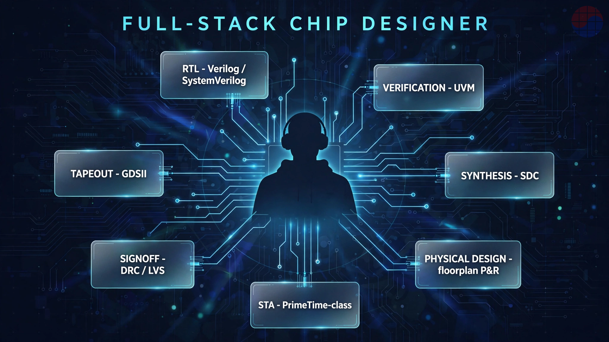
I get to say this because I live on both ends. I build back-end signoff tools for a living — PrimeTime, PrimeShield, PrimePower — and before that, at SiFive Korea, I owned the full RTL-to-GDSII flow on Samsung 5–14nm and taped out 5+ chips (including Rebellions ATOM, FuriosaAI WARBOY, and RHEA). So I'll say it plainly: don't learn from the back. Learn from the front.
Deep Dive: The 7-Stage Roadmap
Stage 1. Digital Logic — The Foundation of Everything
What to learn: Boolean algebra, combinational logic (muxes, decoders, encoders), sequential logic (flip-flops, latches), finite state machine (FSM) design, Karnaugh maps, and the basics of timing — setup and hold as concepts. This is not math class. It's building an instinct for "what happens in one clock tick."
The beginner trap: "I took digital logic in undergrad, skip." The people who skip this are the ones who can't debug a CDC bug three years later because they never drew an FSM by hand. Being lectured at is not the same as knowing. Draw the FSM. Sketch the timing diagram by hand.
How long: 2–4 weeks. Validate with HDLBits combinational/sequential problems.
Next step: the VLSI Foundations roadmap (64 skills) in edu.vlsi.kr's 44-path career map.
Stage 2. RTL Design — Learning the Language of Chips
What to learn: The synthesizable subset of Verilog/SystemVerilog, blocking vs non-blocking assignment, FSM coding styles, parameterizable module design, basic interfaces (AXI-lite level), and CDC fundamentals. Simulators: Icarus Verilog. Lint: Verilator. Waveforms: GTKWave. All free.
The beginner trap: Writing Verilog like software. A for loop in RTL doesn't "execute repeatedly" — it replicates hardware. And latch inference: miss a case in an always @(*) block and you get an unintended latch. This is also a classic interview question, for good reason.
How long: 2–3 months. Target project: design a FIFO + arbiter + simple UART controller yourself, and verify each with a testbench you wrote.
Next step: the RTL Design roadmap (64 skills) in edu.vlsi.kr's 44-path career map.
Stage 3. Verification — Proving the Chip Is Correct
What to learn: SystemVerilog testbenches, coverage-driven verification (code + functional coverage), constrained-random stimulus, and the basic UVM structure (agent, sequencer, driver, monitor, scoreboard). There is an industry saying that roughly 70% of ASIC effort goes to verification. Verification is not a side quest — it is most of the job.
The beginner trap: Thinking "verification = running tests." Random tests without a coverage plan are just button-pressing. Real verification starts by writing down what must be proven (the coverage plan) and then closing it. And a verification engineer who can't read RTL can file bugs but can't explain root causes. That's why Stage 2 comes first.
How long: 2–4 months. Target: attach a UVM-lite style testbench to the UART from Stage 2 and close functional coverage to 100%.
Next step: the Design Verification roadmap (64 skills) in edu.vlsi.kr's 44-path career map.
Stage 4. Synthesis — Translating RTL to Gates
What to learn: How logic synthesis works (technology mapping), SDC timing constraints (create_clock, set_input_delay, set_output_delay), lint and CDC checks, and the line between synthesizable and unsynthesizable coding styles. Open-source: Yosys. Industry: Design Compiler-class tools.
The beginner trap: "The synthesis tool will fix my unsynthesizable code." It won't. It doesn't guess your intent. A latch you wrote in Stage 2 becomes a latch in gates in Stage 4. Learning synthesis rewrites how you write RTL — which is the empirical proof of why the front has to come first.
How long: 1–2 months. Target: synthesize your Stage 2 design to Sky130 cells with Yosys and read the timing report with understanding.
Next step: the Synthesis / Constraints / Front-End Implementation roadmap (64 skills) in edu.vlsi.kr's 44-path career map.
Stage 5. Physical Design — Putting Gates on Silicon
What to learn: Floorplan, power delivery network (PDN), placement, clock tree synthesis (CTS), routing, and congestion analysis. Open-source: OpenROAD/OpenLane — a flow used in 600+ real tapeouts. Industry: ICC2/Innovus-class tools.
The beginner trap: Learning PD as "flow button-pushing." Real PD skill lives in floorplan and congestion judgment. When congestion blows up, the answer isn't "the tool will handle it" — it's deciding whether the problem is RTL structure, floorplan, or placement density. That judgment only exists if you know Stages 2–4. A PD engineer who doesn't understand RTL structure is helpless in front of congestion.
How long: 2–4 months. Target: push a small block (e.g., your Stage 2 arbiter) through OpenLane all the way to GDSII.
Next step: the RTL-to-GDS / Physical Implementation roadmap (97 skills) in edu.vlsi.kr's 44-path career map.
Stage 6. STA / Signoff — Proving the Timing Is Correct
What to learn: Setup/hold timing, OCV/AOCV/POCV variation models, crosstalk delay and noise, multi-corner multi-mode (MCMM) analysis, and ECO (engineering change order). Open-source: OpenSTA. Industry standard: PrimeTime — the tool I build every day.
The beginner trap: Obsessing over one number (WNS = 0). With wrong constraints, a "clean" report is a lie. Declaring false paths aggressively to make timing look closed is the pattern interviewers hate most — and the pattern that kills chips in production. STA is not reading reports; it's judging whether the report deserves trust. That judgment comes from Stage 2 (understanding RTL structure) and Stage 4 (understanding constraints).
How long: 2–3 months. Target: analyze your Stage 5 block's timing with OpenSTA and distinguish real violations from false ones.
Next step: the STA / Timing Signoff roadmap (88 skills) in edu.vlsi.kr's 44-path career map.
Stage 7. Tapeout — Shipping to the Fab
What to learn: DRC/LVS, antenna rules, metal fill, the ECO freeze process, and GDSII handoff with mask data prep. The open-source route is DRC/LVS with Magic/KLayout.
The beginner trap: "GDSII is out, we're done." You're not done until post-silicon bring-up shows the chip alive. Tapeout isn't the finish line — it's the exam where silicon grades the sum of your judgments in the previous six stages.
How long: 1–2 months (as a learning stage). Target: take your Stage 5–6 block to DRC/LVS clean.
The edu.vlsi.kr Learning Track: Where to Go Next
This article is the map. The climb continues at VLSI Korea Education. Each stage has a matching career roadmap waiting.
- VLSI Korea Education home — the entry point to the RTL2GDS learning platform, linking roadmaps, tutorials, interviews, and practice sections.
- The full 44-path semiconductor career map — the roadmap collection that maps 1:1 onto this article's 7 stages. Walk it in order: RTL Design (64 skills) → Design Verification (64 skills) → Synthesis / Constraints / Front-End Implementation (64 skills) → RTL-to-GDS / Physical Implementation (97 skills) → STA / Timing Signoff (88 skills). Each roadmap connects staged skills to verified learning resources.
- Semiconductor education events calendar — offline seminars and workshops. When you're stuck alone, asking in person is the fastest debugger there is.
One honest note. Today edu.vlsi.kr has per-role career roadmaps, but there is not yet a single tutorial track that walks these 7 stages in order — a hands-on "RTL-first lab track" (Yosys synthesis lab, OpenLane PD lab, OpenSTA timing lab, sequenced in tapeout order). The funnel this article opens will be complete when that page exists. Until then, the best route is walking the five roadmaps above in order.
Chase's Take
I make back-end tools for a living. PrimeTime, PrimeShield, PrimePower — the very last stage of the flow, signoff. And yet the strongest advice I give juniors is "learn from the front." Sounds contradictory? It isn't. The longer you live in the back end, the more viscerally you understand how much the front end matters.
At SiFive Korea, I owned the entire flow from RTL to GDSII on Samsung 5–14nm. Rebellions ATOM, FuriosaAI WARBOY, RHEA — across 5+ tapeouts, one lesson kept repeating: wherever you're stuck, the answer is always upstream. Timing won't close? Tear apart the RTL structure. Congestion exploding? Half the time it's the microarchitecture, not the floorplan. A back-end engineer who doesn't know the front chases symptoms.
"You have to touch the whole flow." That's my doctrine. It doesn't mean don't specialize — depth can come later. But spend your first year or two walking all seven stages once. That one lap becomes your compass for life. The engineer who can see the whole chip from wherever they stand — that's the most expensive engineer in the market.
FAQ
Q1. Can I start with verification or STA without knowing RTL? You can. Bootcamps teach it that way. But there's a price. A verification engineer who can't read RTL files bugs without diagnosing root causes; an STA engineer just says "ask the RTL team" in front of every violation. You can start there, but you'll end up walking back to the front anyway. Going in order from the start is the shortcut.
Q2. Can I practice all 7 stages with open-source tools only? Yes. Icarus Verilog/Verilator (simulation) → Yosys (synthesis) → OpenROAD/OpenLane (PD) → OpenSTA (STA) → Magic/KLayout (DRC/LVS) + the Sky130 PDK. OpenROAD has been used in 600+ real tapeouts via the Efabless MPW shuttle program. Industry tools (Design Compiler, ICC2/Innovus, PrimeTime) have different buttons, but the concepts you learn are the same.
Q3. How long does the full 7-stage pass take? 12–18 months of self-study is realistic. Roughly: digital logic 2–4 weeks, RTL 2–3 months, verification 2–4 months, synthesis 1–2 months, PD 2–4 months, STA 2–3 months, tapeout 1–2 months. The bar per stage is "one working deliverable." Skip a stage to go faster and you'll pay double on the way back.
Q4. Does this order apply to analog or memory design too? This roadmap is calibrated for the digital front-end-to-back-end axis. Analog, memory, and packaging are separate axes. That said, digital-logic and RTL instincts help analog engineers too, and STA/signoff concepts connect directly to memory interface (DDR, HBM controller) design. Different axis, same principle: understanding the front saves the back.
This article is a learning guide, not career advice. Tools and flows change — cross-check with current official documentation.