VLSI Korea
Samsung Goes Up, SK hynix Goes Sideways: zHBM, HBF and the Fight for the Memory Layer After HBM
At SEDEX 2026 Samsung unveiled zHBM stacked on the GPU while SK hynix proposed HBF, a new flash tier between HBM and DRAM. Why the inference bottleneck moved from speed to distance — and what decides who wins the layer after HBM.


The HBM race is not over, but at SEDEX 2026 both Korean memory makers stopped arguing only about the current generation and started claiming the layer after HBM. Samsung Electronics and SK hynix used the exhibition in Seoul (October 14–16, 2026) to show two opposite answers to the same problem. Samsung's zHBM stacks memory vertically on top of the GPU. SK hynix's HBF inserts an entirely new memory tier between HBM and DRAM. The conclusion matters more than the mockups: the bottleneck in AI inference has moved from raw speed to distance, and the next memory war will be won by whoever defines the new tier — its physics, or its standard.
That is the strategic read of SEDEX 2026, the 28th Semiconductor Exhibition held at COEX in Seoul with about 300 companies participating. Both companies also displayed HBM4E, the seventh-generation HBM that actually ships and earns money next. But the products on the keynote slides were not HBM4E. They were two competing architectures for what sits around it.
What was actually unveiled
HBM4E, side by side. Samsung and SK hynix both put HBM4E at the front of their booths (reported October 15, 2026). Samsung's HBM4E combines 10nm-class sixth-generation (1c) DRAM with a base die built on a 4nm foundry process. Per-pin data transfer speed is 14 Gbps to 16 Gbps, more than 20% higher than HBM4, and maximum memory bandwidth reaches 3.6 TB/s. HBM4E is the near-term product: qualification, yield and customer allocation decide 2027 revenue.
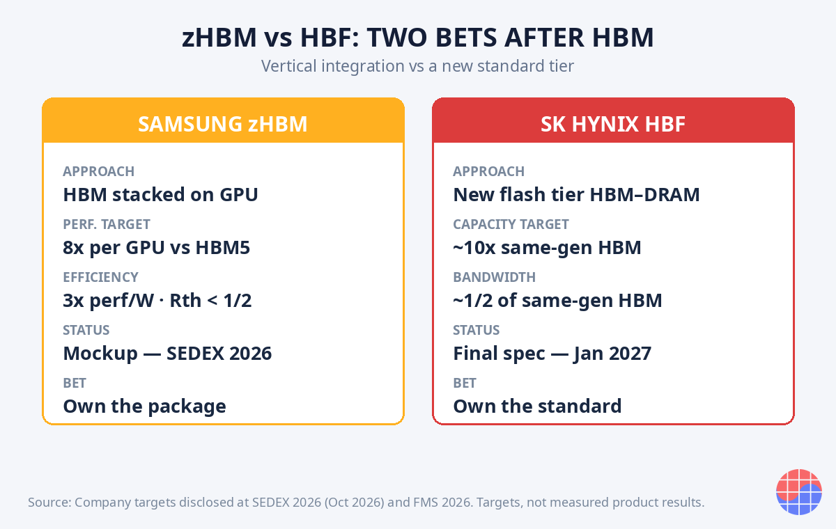
Samsung zHBM: go up. Samsung displayed a mockup of zHBM, which stacks HBM vertically on top of the GPU itself. The targets, first presented at FMS 2026 in August, are aggressive: up to 8x performance per GPU versus HBM5, up to 3x performance per watt, and thermal resistance cut to less than half. The logic is physical. If data movement is the cost, the shortest possible path between compute and memory is to put the memory directly above the compute die.
SK hynix HBF: go sideways. SK hynix's answer is HBF, High Bandwidth Flash. Instead of making HBM taller, HBF creates a new tier between HBM and DRAM, built on NAND flash. The target profile is the mirror image of HBM: bandwidth at about half of a same-generation HBM, but capacity at roughly 10x. SK hynix has started standardization work with SanDisk, published a first specification in August 2026, and plans a final HBF specification in January 2027 with partners including Google, with product launch targeted for the end of 2027.
| Samsung zHBM | SK hynix HBF | |
|---|---|---|
| Approach | Stack HBM vertically on top of the GPU | Insert a new flash tier between HBM and DRAM |
| Target | Up to 8x performance per GPU vs HBM5, up to 3x perf/W, thermal resistance under half | About half the bandwidth of same-gen HBM, about 10x the capacity |
| Status (Oct 2026) | Mockup shown at SEDEX 2026; first shown at FMS 2026 in August | First spec published Aug 2026; final spec planned Jan 2027; launch targeted end of 2027 |
| Core bet | Physics: shorten the distance | Standard: define the new tier |
Why the bottleneck moved from speed to distance
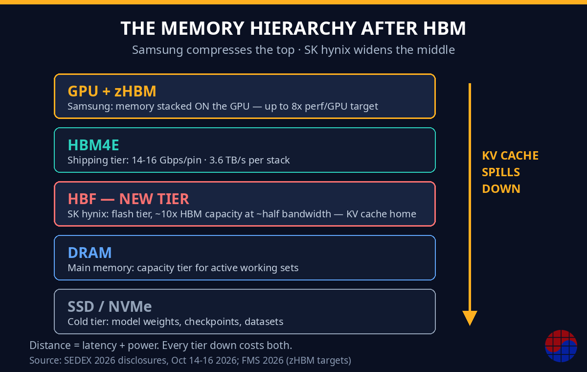
SK hynix President Ahn Hyun, head of development, put the diagnosis in his SEDEX keynote: data movement between memory tiers has itself become the most important bottleneck. He projected AI infrastructure scale growing to roughly 20x today's level by 2030. In the inference era, context keeps getting longer, and the KV cache that holds that context spills down the hierarchy — from HBM to DRAM to SSD. Every step down is distance, and distance is latency and power.
This is why a flash-based tier is suddenly plausible. Inference is read-heavy: the same weights and cached context are read over and over, while writes are comparatively rare. NAND flash, long dismissed for this layer because of weak write endurance and write speed, becomes a weapon again when the workload mostly reads. HBF is not trying to beat HBM at HBM's game. It is trying to make the spill cheaper — to give the KV cache a home that is far larger than HBM and far closer than an SSD.
zHBM attacks the same equation from the other end. If the top of the hierarchy is where the hottest data lives, then collapse the distance at the top to nearly zero: memory on top of compute. Samsung is not proposing a new tier. It is proposing to delete the distance inside the existing top tier.
The engineer's view: both bets have a hard problem, and it is not the headline one
Strip away the keynote language and each architecture has a specific, unglamorous engineering risk.
For zHBM, the risk is heat and yield, in that order. Stacking memory on top of a GPU means the memory sits in the GPU's thermal path. Samsung's own target — thermal resistance cut to less than half — is an admission that the heat path is the design problem, not a footnote. Then comes package economics: when memory and a large GPU die are integrated that tightly, known-good-die discipline and package yield decide whether the part is a product or a science project. And there is an ownership question no mockup answers: the GPU belongs to the customer. Stacking your memory on top of someone else's flagship die is an integration negotiation as much as a technology.
For HBF, the risk is not the NAND. It is everything around it: the controller, the firmware, the software stack that decides what lives in HBF versus DRAM, and — above all — adoption. A new memory tier only exists if accelerator designers, hyperscalers and the software ecosystem agree to address it. That is precisely why SK hynix is running a standardization track with SanDisk and hyperscaler participation before the product exists. The January 2027 final specification is not paperwork. It is the product's real launch event.
There is also a timing-and-signoff reality that applies to both. Neither zHBM nor HBF changes what has to close timing, pass qualification and ramp in 2027. HBM4E does. Engineers should read SEDEX 2026 as two roadmap claims staked early — deliberately early, because tiers and standards are claimed before they are built, not after.
The business view: integration versus standard
This is where the two strategies diverge as business models, not just as engineering.
Samsung's bet is vertical integration. zHBM only makes sense as a bundle: memory, foundry base die and advanced packaging from one supplier. Samsung's HBM4E already shows the pattern — 1c DRAM on a 4nm foundry base die. Extend that logic and Samsung is selling an integrated memory-compute package, shortening the customer's development cycle and capturing more of the stack's value per accelerator. Samsung is also looking further out, with HBM5 mass production targeted for 2029 and hybrid bonding intended to break past 20-layer stacks, as reported plans. Integration is Samsung's structural advantage: it is the only company that owns memory, leading-edge foundry and packaging at scale under one roof.
SK hynix's bet is the standard. HBF's bandwidth target is deliberately unremarkable — half of HBM. Its capacity target is the point, and its standardization timeline is the strategy. In semiconductors, standards outlive manufacturing leads. A one-generation speed lead lasts a year. The company that defines a new tier's specification helps allocate that market for a decade, because every controller, accelerator roadmap and software stack built to the spec reinforces the position. SK hynix is pairing with SanDisk on the specification and bringing hyperscalers into the January 2027 finalization. That is not a memory launch plan. It is a coalition-building plan.
Both can be right, because they attack different layers. zHBM raises the ceiling of the top tier. HBF widens the middle. An AI accelerator in 2028 could plausibly use both. But they cannot both own the narrative of "what comes after HBM" — and narrative, in a standards fight, converts directly into design wins.
What still makes the money: HBM4E, and a market that is not slowing
The counterweight to both roadmap bets is the present tense. Demand for the current generations is still outrunning supply. TSMC reported third-quarter 2026 results on October 15: revenue of NT$1.494 trillion (US$46.7 billion) and net income of NT$763.06 billion, up 68.7% year over year, with management stating that AI demand still exceeds its supply capability. Industry views reported around SEDEX held that the HBM-driven memory shortage could persist into 2028.
So the cash register in 2027 is HBM4 and HBM4E qualification — who passes, at what yield, with what allocation. zHBM and HBF decide 2028 and beyond. Investors and customers should weight them accordingly: the new tiers are options on the post-HBM hierarchy, priced today mostly as keynote claims, with HBF's January 2027 specification and any zHBM move beyond mockup as the first hard checkpoints.
One more pressure runs underneath: commodity DRAM. Chinese maker CXMT continues to close ground in conventional DRAM. The Korean strategy visible at SEDEX is coherent against that backdrop — concede the commodity layer gradually, and own the layers above it: HBM today, and either the integrated package (Samsung) or the new standard tier (SK hynix) tomorrow.
What to watch
- January 2027: the HBF final specification. Who signs on — and whether accelerator and hyperscaler names attach to it — tells you if HBF is a tier or a presentation.
- HBM4E qualification results. 14–16 Gbps per pin and 3.6 TB/s are claims until customers qualify parts at yield.
- zHBM beyond the mockup. A named GPU partner or a thermal solution disclosure would move zHBM from architecture slide to program.
- HBM5 signals. Samsung's reported 2029 mass-production target and hybrid bonding path show how far the vertical bet extends.
- CXMT in commodity DRAM. The faster the commodity layer commoditizes, the more valuable the tiers above it become.
FAQ
What is SK hynix HBF?
HBF (High Bandwidth Flash) is a proposed new memory tier between HBM and DRAM, built on NAND flash. As disclosed at SEDEX 2026 (October 14–16, 2026), it targets about half the bandwidth of a same-generation HBM at roughly 10x the capacity, aimed at inference workloads such as KV cache. SK hynix and SanDisk published a first specification in August 2026; a final specification is planned for January 2027, with product launch targeted for the end of 2027.
What is Samsung zHBM?
zHBM is Samsung's proposal to stack HBM vertically on top of the GPU. First shown at FMS 2026 in August and displayed as a mockup at SEDEX 2026, it targets up to 8x performance per GPU versus HBM5, up to 3x performance per watt, and thermal resistance of less than half. These are company targets, not measured product results.
How is HBM4E different from HBM4?
HBM4E is the seventh-generation HBM shown by both Samsung and SK hynix at SEDEX 2026. Samsung's version pairs 1c DRAM with a 4nm foundry base die, running at 14–16 Gbps per pin — more than 20% above HBM4 — for up to 3.6 TB/s of bandwidth per stack.
Which approach wins, zHBM or HBF?
They solve different problems and could coexist. zHBM compresses distance at the top of the hierarchy through vertical integration; HBF widens the middle of the hierarchy and depends on standardization, with a final specification due in January 2027. The nearer-term revenue for both companies still comes from HBM4 and HBM4E, amid a memory shortage that industry views expect could persist into 2028.
Disclosure: This analysis is based on public disclosures and reporting from SEDEX 2026 (October 14–16, 2026), FMS 2026, and TSMC's third-quarter 2026 results (October 15, 2026). Performance and capacity figures for zHBM and HBF are company targets for products not yet in mass production. The author holds no position in the companies discussed. Figures are as of October 18, 2026.