VLSI Korea
From Verification to Design: A Transition Guide
From Verification to Design: A Transition Guide 30-Second Summary * DV (Design Verification) is the largest hiring funnel in front-end chip design. It is an easy entry, but moving to RTL design takes a deliberate transition. * What transfers directly: testbench thinking, coverage methodology, protocol knowledge like AMBA/AXI, and debugging discipline. * What does not: microarchitecture design, a timing-closure


From Verification to Design: A Transition Guide
30-Second Summary
- DV (Design Verification) is the largest hiring funnel in front-end chip design. It is an easy entry, but moving to RTL design takes a deliberate transition.
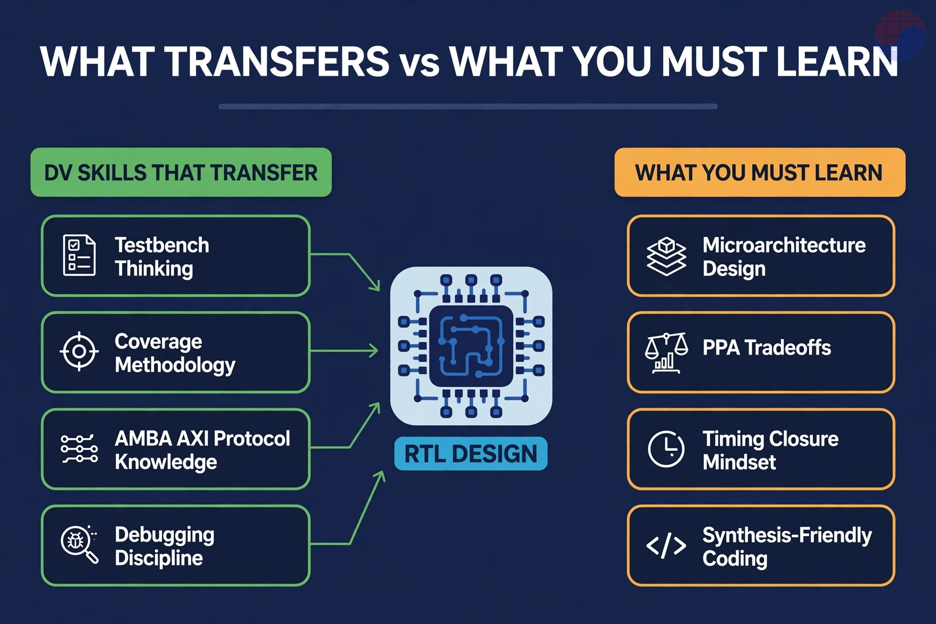
- What transfers directly: testbench thinking, coverage methodology, protocol knowledge like AMBA/AXI, and debugging discipline.
- What does not: microarchitecture design, a timing-closure mindset, PPA tradeoff intuition, and synthesis-friendly coding.
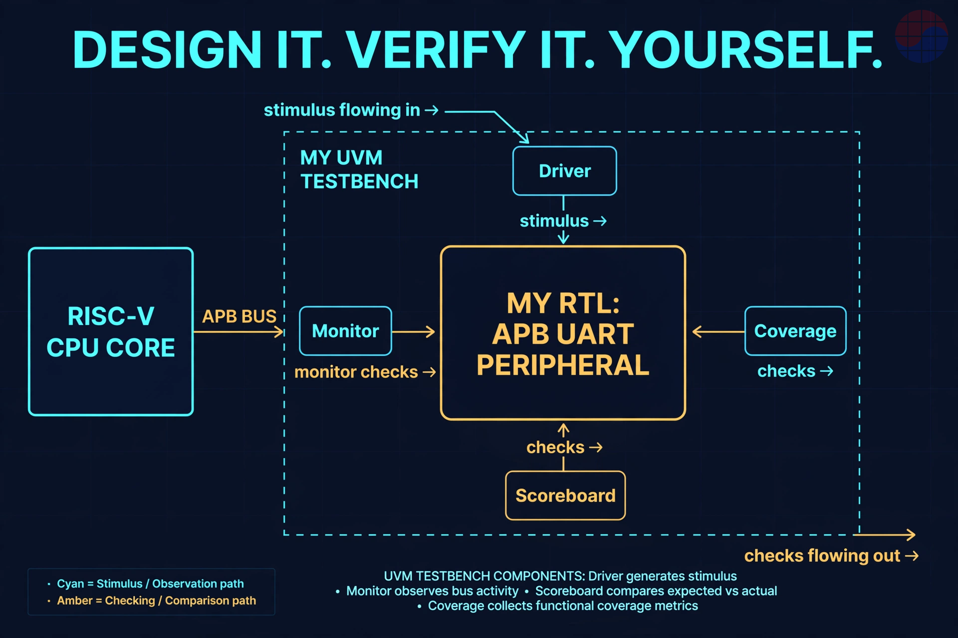
- The most convincing portfolio is one small RISC-V peripheral that you both designed AND verified yourself. Your UVM testbench proves your DV background.
- In interviews, frame DV as a design asset, not a detour: "I spent N years finding other people's RTL bugs, so I write RTL that doesn't have them."
Intro: Why move from DV to design?
Look at front-end hiring and one pattern repeats: DV hires the most people. The reason is straightforward. Wilson Research Group found that logic verification effort can consume up to 70% of total project time on large chip programs. Bigger chips need more verification engineers, so DV is the widest door for juniors entering the industry.
But many who walk through that door ask the same question two or three years later: "I want to try design now. Does my DV experience help, or do I start over?"
The honest answer is both. About half of your DV skill set transfers directly to design; the other half has to be learned on purpose. This guide draws that line precisely and turns it into a 6-month plan you can actually execute.
Start with market data. In India, RTL design engineers start around 6 to 8 LPA and reach 18 to 30 LPA with 5+ years of experience. DV engineers track closely and sometimes exceed RTL pay at senior levels, because verification expertise has become one of the tightest skill bottlenecks as chip complexity grows. In the US, actual 2026 Q3 postings from a large AI chip company listed a mid-level RTL design role at 138k to 197k USD base plus 15% bonus, and senior roles up to 163k to 237k USD. Moving to design is a move that pays. But the door opens on merit.
1. What transfers from DV to design
1.1 Testbench thinking: reading specs like an adversary
DV engineers read specs asking "how would I break this?" That is the most valuable habit a designer can have. Someone who writes RTL already picturing corner cases writes fundamentally different code from someone who assumes the testbench will catch everything. This is the number one reason DV veterans write good RTL.
1.2 Coverage methodology: knowing what "done" means
One of the hardest things for junior designers is judging "is this finished?" DV engineers are trained to define "done" with functional and code coverage. That judgment transfers directly to splitting a microarchitecture into blocks and setting completion criteria for each.
1.3 Protocol knowledge: hands that know AMBA/AXI
Half of SoC design is interfaces. If you have internalized AXI4, AXI-Lite, and APB handshakes, ordering rules, and outstanding transactions through verification, you will not get lost designing a peripheral interface. Bus protocols appear on virtually every RTL design job posting's required-skills list. From DV, you already own this.
1.4 Debugging discipline: waveform forensics
Finding bugs across millions of waveform cycles transfers directly to RTL debug. One difference: in DV you found other people's bugs; in design you find your own. It stings more, but the skill is identical.
2. What DV experience does not cover
Be honest with yourself. These four do not come from DV alone. This is the real curriculum of the transition.
2.1 Microarchitecture design: thinking in structures, not stimuli
DV verifies a given structure. Design chooses the structure. For the same FIFO, the depth, cut-through vs. store-and-forward, and where to handle backpressure are microarchitecture decisions that hit throughput, latency, and area simultaneously. In DV you evaluated these decisions; you never made them. Until you hand-design pipelines, arbiters, and FSM encodings, this muscle does not exist.
2.2 Timing-closure mindset: RTL that meets a clock
In a testbench, 1 GHz or 10 MHz makes no difference as long as functionality is correct. In silicon, your RTL becomes gates that must meet setup and hold in a fixed clock period. The most common mistake DV engineers make writing their first RTL is stacking combinational logic too deep. Hearing "functionally correct but timing fails" in a design review is the first gate of the transition. Thinking in critical paths and splitting pipeline stages has to be trained deliberately.
2.3 PPA tradeoff intuition: the price of every line
Power, Performance, Area. Every design decision pays on these three axes. In DV, PPA was someone else's problem. In design, your always block shows up as a number in the area report. Whether you just instantiate a 32-bit multiplier or think about Booth encoding, where you put clock gating, is where skill shows.
2.4 Synthesis-friendly coding: the simulation-synthesis gap
Code that simulates fine does not always synthesize as intended. Latch inference, incomplete case statements, and simulation-synthesis mismatches are the areas where DV-only engineers are most exposed. Build the habit of running lint and CDC checks right after writing RTL. There is a reason linting, CDC, RDC, and LEC appear on nearly every real job posting's required skills.
3. The 6-month plan: a month-by-month execution table
Assumes 8 to 10 hours per week of side study, calibrated for a working DV engineer.
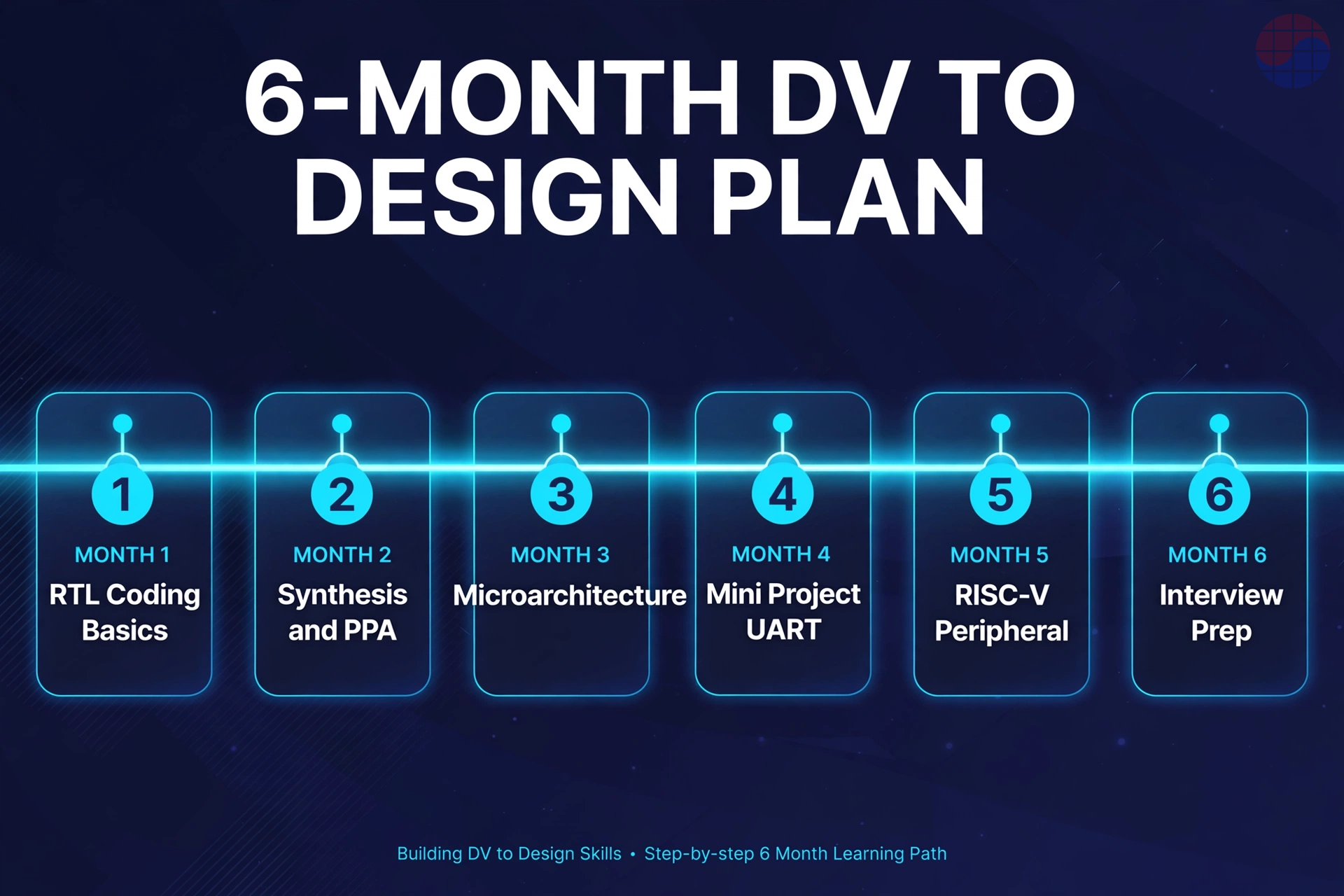
Month 1 — RTL Coding Basics. Relearn Verilog as a writing language, not a reading language. Master the blocking vs. non-blocking traps, three FSM styles, and parameterized module design. Goal: write a 500-line lint-clean module yourself.
Month 2 — Synthesis and PPA. Synthesize what you wrote in Month 1. Open tools (Yosys, OpenLane) are enough. Learn to read area and timing reports, and write the same function three ways to compare PPA. Goal: be able to say how many gates your code costs.
Month 3 — Microarchitecture. Hand-design FIFOs, arbiters, crossbars, and pipeline stages. Compute throughput, latency, and area for each and document the tradeoffs. Goal: answer "how did you size the FIFO depth?" with numbers.
Month 4 — Mini Project: UART. Write an APB UART controller from spec. Small but real: register map, interrupts, baud rate generator. Goal: one GitHub repo with spec, RTL, and docs.
Month 5 — RISC-V Peripheral. Attach the Month 4 UART to a RISC-V core and verify it yourself with your own UVM testbench. This is the heart of the plan, the moment your DV background proves itself in the portfolio. Target 95%+ coverage and document the self-found bugs.
Month 6 — Interview Prep. Collect 100 design-focused interview questions and write out answers. Organize microarchitecture rationale, PPA tradeoff stories, and timing-closure experience in STAR format. Goal: answer "why does a DV person want design?" in a 90-second story.
4. Portfolio projects: design it, verify it, prove it
Hiring managers look for one thing in a DV-background portfolio: "can this person write RTL?" And a second question follows for DV candidates: "can they actually verify?" One project answering both is the optimal structure.
Recommended project: APB UART Peripheral + self-built UVM testbench
It looks simple, but the evaluation points land exactly.
- Design side: register map, TX/RX FSMs, baud rate generator, interrupt logic, APB slave interface. Interviewers will ask for the rationale behind microarchitecture decisions. Be ready to answer why the FIFO depth is 16, with numbers.
- Verification side: your home turf. UVM driver/monitor/scoreboard, functional coverage, assertions. Attach the coverage report. Documenting three bugs you found in your own RTL takes this repo to a different level from tutorial output.
- PPA side: attach synthesized area and timing reports. Few candidates know the price of their own design.
Structure the repo like this: docs/ (spec, microarchitecture decision log), rtl/, tb/ (UVM), synth/ (reports). Put three lines at the top of the README stating what this project proves. Hiring managers decide in 30 seconds.
5. Interview framing: DV is an asset, not a detour
The interviewer's question is fixed: "Can a DV person do design?" Answer defensively and you lose. Frame it offensively.
Core message: "I spent N years finding other people's RTL bugs. So I know how to write RTL that doesn't have them."
It works because it is specific. Then attach evidence:
- "Here are the three worst RTL patterns I saw in verification. First... which is why in my code..."
- "Having done coverage closure, I design verification-friendly structures from the start. For example..."
- "After debugging an AXI ordering bug, here's how I manage outstanding transactions when I design a master..."
Never do this:
- Don't trash DV. "Verification was boring" is the worst possible answer. The right posture: someone who knows verification's value becoming a designer.
- Don't stop at "I can write RTL too." Prove it with the portfolio repo link.
- Don't dodge timing and PPA questions. If you don't know, say so honestly: "Still learning, and here's how I'm approaching it." Design interviewers detect bluffing fastest.
Common design interview questions (DV switchers should over-prepare these):
- Blocking vs. non-blocking: when to use which, and what changes in synthesis?
- FIFO depth calculation: write at 100 MHz, read at 50 MHz, burst of 64 — minimum depth?
- CDC: the MTBF concept of a 2-flop synchronizer and its limits; when is a handshake required?
- In AXI4, under what conditions is out-of-order completion allowed?
- Where was the critical path in your block, and how did you fix it?
Number 5 is the real question. If you never hit a timing problem in your portfolio project, you cannot answer it. That is why the Month 2 synthesis practice is mandatory.
Learning roadmap on edu.vlsi.kr
Each step of this guide maps directly onto edu.vlsi.kr roadmaps. Walk them in order.
- RTL design roadmap — the curriculum for Months 1 to 3, from Verilog basics to microarchitecture.
- Verification roadmap — the weapon you already have. UVM, coverage, formal. Use it to audit your current position before the switch.
- RTL2GDS full-flow roadmap — the whole picture from RTL to a chip. The map behind the "touch the entire flow" philosophy.
- RTL design salary data — role-by-role compensation data. Verify the economics of the transition in numbers.
Chase's Take
Full disclosure: I am not from DV. At SiFive Korea I owned RTL-to-GDS end to end and taped out 5+ times on Samsung 5 to 14nm. Now I am a Staff Product Engineer at Synopsys building STA and signoff tools like PrimeTime, PrimeShield, and PrimePower. I build back-end tools, but I always tell juniors to learn front-to-back: RTL first, then verification, then synthesis and PD, then STA and signoff. You have to touch the entire flow.
So when I look at people who entered through DV-first, I see two types. One stays in verification. The other uses verification as a springboard back to the front and learns RTL properly. Five years later, the second type is the far stronger engineer. The reason is simple: someone who has caught hundreds of bugs writes different RTL from the start. The bad design patterns seen in verification get internalized, and you avoid them without thinking.
But don't fool yourself. DV years do not automatically become design skill. Making STA tools doesn't make me good at STA, and verifying for years doesn't make you good at writing RTL. You become a designer by architecting microarchitecture yourself, getting burned by area reports after synthesis, and chasing timing violations overnight. The 6-month plan in this guide is exactly that process, compressed.
One last thing. Don't treat DV as a waiting room on the way to design. Verification eats more than half of a chip project's time; it is real engineering. You already own half of a designer. Fill the other half in six months.
FAQ
Q1. I have 3 years of DV experience. Should I apply as a design new grad?
A. Don't throw away your leverage by applying as a new grad. Apply to design positions carrying your DV years. Three years of DV beats zero years of design. Prove RTL ability with a portfolio and frame DV as verification-aware design capability. Don't surrender your DV seniority in salary negotiation either.
Q2. Shouldn't I just go deeper into UVM? Senior DV pays more, I hear.
A. That is true in many cases. Senior DV supply is tight, and compensation sometimes exceeds RTL. So this guide is not "leave DV" but "expand your options." A DV engineer who can write RTL also opens paths to verification lead, design manager, and architect. The transition is an expansion, not an escape.
Q3. Can I build the portfolio on FPGA?
A. Yes, and it is recommended. RTL that you actually ran on an FPGA is more convincing than simulation-only work. But running on FPGA does not mean ASIC timing is solved. Submit it with the synthesis report.
Q4. Is 6 months realistic alongside a full-time job?
A. Yes, at 8 to 10 hours a week for a working DV engineer. Subtract what you already know from DV (protocols, debugging, coverage) and only three things are new: microarchitecture, synthesis and PPA, and timing intuition. The Month 5 self-verification project goes fast because it is your day-job skill.
This is a career guide and does not guarantee any hiring outcome. Salary figures are from public sources and may differ from actual compensation.
Sources: Wilson Research Group 2022 findings via SemiWiki; 2026 Siemens/Wilson study via SemiWiki; India salary data via Futurense 2026 salary guide and entri.app; US 2026-Q3 RTL postings via hardwareifai; JobzMall; entry-point data via techgig and Futurense 2026 guide.