VLSI Korea
SK hynix–Intel Talks, Winbond Deal and MLPerf | Daily Silicon
Eleven semiconductor developments: SK hynix clarifies US memory talks, Winbond signs an Infineon deal, MLPerf 6.1, Altera IPO plans and Rebellions in Japan.


🆓 Free article · Anyone can read this article for free
Executive Summary
- SK hynix–Intel US memory talks remain unconfirmed
- Winbond signs $1.12 billion deal for Infineon NOR and F-RAM
- MLPerf 6.1 adds RAG and agent tests; Rubin remains Preview
- IBM’s Anderon finalizes up to $1 billion in CHIPS support
- Altera parent confidentially submits US IPO draft
- Astera expands Leo to connect stranded memory capacity
- Google, NVIDIA and Emerald AI launch flexible-power alliance
- China’s CNY30 trillion target covers electronics, not chips alone
- Viewtrix forms optical-link and UCIe IP subsidiaries
- onsemi ties AI power and automotive to shared technology platforms
- Rebellions and ai& plan Japan inference deployment
01 SK hynix–Intel US memory talks remain unconfirmed
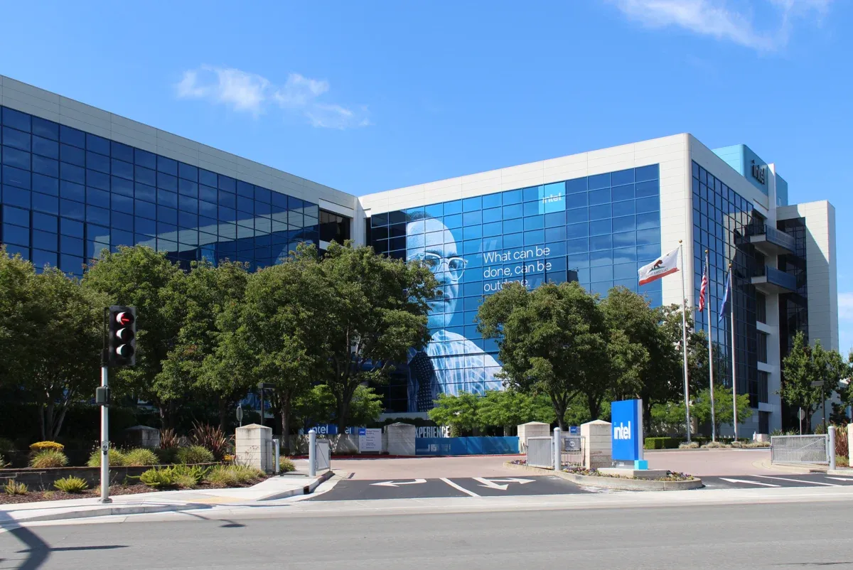
TL;DR Reuters reported talks over producing SK hynix memory wafers in the US with Intel. SK hynix said it is exploring options but has finalized no specific plans or arrangements.
The official company response says neither the reported plant-lease scenario nor a joint venture has been decided. This is reporting about discussions, not a signed US fab contract or confirmed HBM production plan. Investment, product scope and construction timing remain unconfirmed here.
Wafer fabrication differs from packaging. A real agreement would still require process, equipment, staffing and regulatory decisions; an existing building does not itself create a qualified line. Watch for a definitive agreement and product disclosures before treating potential capacity as revenue.
Sources · SK hynix · Yahoo Finance report (2026-09-16)
02 Winbond signs $1.12 billion deal for Infineon NOR and F-RAM
TL;DR Winbond agreed to acquire 100% of Infineon’s NOR Flash and F-RAM business in cash. The $1.12 billion base price is subject to adjustments; closing is expected in the second half of 2027, subject to approvals and other conditions.
Winbond plans to revive the Spansion name and retain a standalone US-headquartered entity. Signing does not mean the assets have already transferred.
This concerns code-storage and specialized nonvolatile memory, not a purchase of a leading DRAM business. Customers will care about long-term supply and support continuity more than the revived brand. Regulatory clearance and the eventual integration plan remain the next checkpoints.
Sources · Winbond (2026-09-16)
03 MLPerf 6.1 adds RAG and agent tests; Rubin remains Preview
TL;DR MLPerf Inference 6.1 adds End-to-End RAG and Edge Agentic Inference tests. NVIDIA Rubin and Vera Rubin NVL72 submissions are Preview results, not equivalent to currently available systems.
The RAG test separates corpus ingestion from answering queries against a vector database. The edge-agent test measures multi-turn workload latency and accuracy. Both move evaluation beyond the speed of a single prompt.
Thirty organizations submitted results. MLCommons lists Ryzen AI Max+ 395, Instinct MI350P and Arc Pro B70 as available, while the new NVIDIA platforms are Preview. Procurement comparisons must match models, accuracy, scenario and accelerator counts; a headline multiplier is not an application-wide speedup.
Sources · MLCommons (2026-09-16)
04 IBM’s Anderon finalizes up to $1 billion in CHIPS support

TL;DR The US Commerce Department signed a final CHIPS R&D award of up to $1 billion for IBM subsidiary Anderon. It supports a 300mm quantum-wafer foundry; the ceiling is not proof that all funding has been disbursed.
This is the final-agreement stage following the May letter of intent. IBM describes a separate $1 billion company investment. These are distinct funding sources, while the letter and final award are stages of the same federal commitment.
Anderon aims to serve the wider quantum ecosystem from Albany. IBM says initial wafers are being processed, which does not establish customer deliveries, production yield or disclosed capacity. Customer qualification and reproducibility matter more than the headline funding ceiling.
Sources · NIST / IBM · IBM announcement (2026-09-16)
05 Altera parent confidentially submits US IPO draft
TL;DR Altera says its parent confidentially submitted a draft Form S-1 to the SEC. Share count and price range remain undetermined, with SEC review, market conditions and other requirements still ahead.
Catch-up on the September 15 announcement, not a new announcement today.
A confidential submission is neither a completed listing nor a priced offering. It starts a process for assessing the programmable-compute business as a public investment; the undisclosed draft cannot support invented financials or valuation.
When a public registration statement appears, revenue mix, customer concentration, R&D spending and cash generation will matter. FPGA exposure to AI alone does not settle investment value. The actual offering structure remains a follow-up question.
Sources · Altera / Business Wire (2026-09-15)
06 Astera expands Leo to connect stranded memory capacity
TL;DR Astera Labs introduced Leo X-Series and Leo 2 E- and P-Series controllers. They target accelerator-side memory tiers, CPU expansion and pooling, and are sampling with hyperscale customers.
Catch-up on the September 15 announcement, not a new announcement today.
X-Series pairs with Scorpio switches to offload KV cache and agent context. E/P use PCIe 6 and CXL 3.2 for DDR4/DDR5 expansion and pooling. An additional memory tier does not enlarge on-package HBM.
Reusing DIMMs requires error management and adequate bandwidth and latency. Published performance claims use an internal Intel GNR, eight-channel DDR5, Gen 5 accelerator and Qwen2.5-32B configuration. Sampling is not broad production deployment.
Sources · Astera Labs (2026-09-15)
07 Google, NVIDIA and Emerald AI launch flexible-power alliance

TL;DR Google, NVIDIA and Emerald AI announced the AI Energy Management Alliance. It advocates standards and policies for flexible data-center demand and faster grid connections.
The proposal is to recognize facilities that can reduce demand when the grid needs relief. Workload changes, storage and colocated generation are possible approaches. A coalition launch is not an approved grid connection or power purchase.
Usable power constrains accelerator deployment. Flexibility could ease that bottleneck, but response time and service quality still require validation. This is an effort to establish an evaluation framework, not capacity already secured.
Sources · NVIDIA / AI Energy Management Alliance (2026-09-16)
08 China’s CNY30 trillion target covers electronics, not chips alone
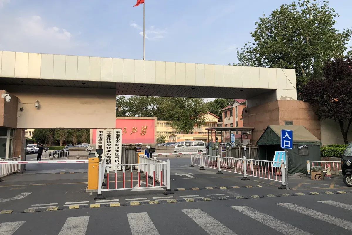
TL;DR MIIT explained China’s 15th Five-Year Plan for electronics and information manufacturing. Its 2030 goals include revenue above CNY30 trillion for enterprises above the designated size and R&D intensity of 3.5%; neither is a chips-only target.
Catch-up on the September 15 announcement, not a new announcement today.
Integrated circuits, components, materials, measurement equipment, photonics and AI hardware all feature. Treating the aggregate goal as semiconductor sales or committed equipment orders changes its scope.
Domestic suppliers may gain qualification opportunities, but budgets, procurement and process adoption stand between policy and revenue. Implementation and customer adoption remain the useful follow-up evidence.
Sources · China MIIT (2026-09-15)
09 Viewtrix forms optical-link and UCIe IP subsidiaries
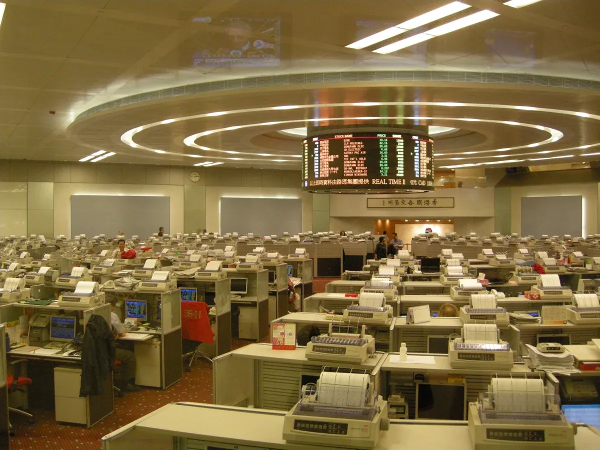
TL;DR Viewtrix disclosed two controlled subsidiaries for optical interconnects and UCIe IP. Both remain in early R&D, without volume products or revenue.
Catch-up on the September 15 announcement, not a new announcement today.
Each has registered capital of CNY10 million, with Viewtrix holding 55%. One targets Micro-VCSEL optical I/O; the other starts with UCIe interconnect IP. These are separate development efforts, not a finished platform.
Private financing is still under negotiation and due diligence. The filing anticipates no material near-term financial contribution. Technical validation, IP customers and signed financing documents are the next evidence to watch.
Sources · Viewtrix filing reproduced by CFI (2026-09-15)
10 onsemi ties AI power and automotive to shared technology platforms
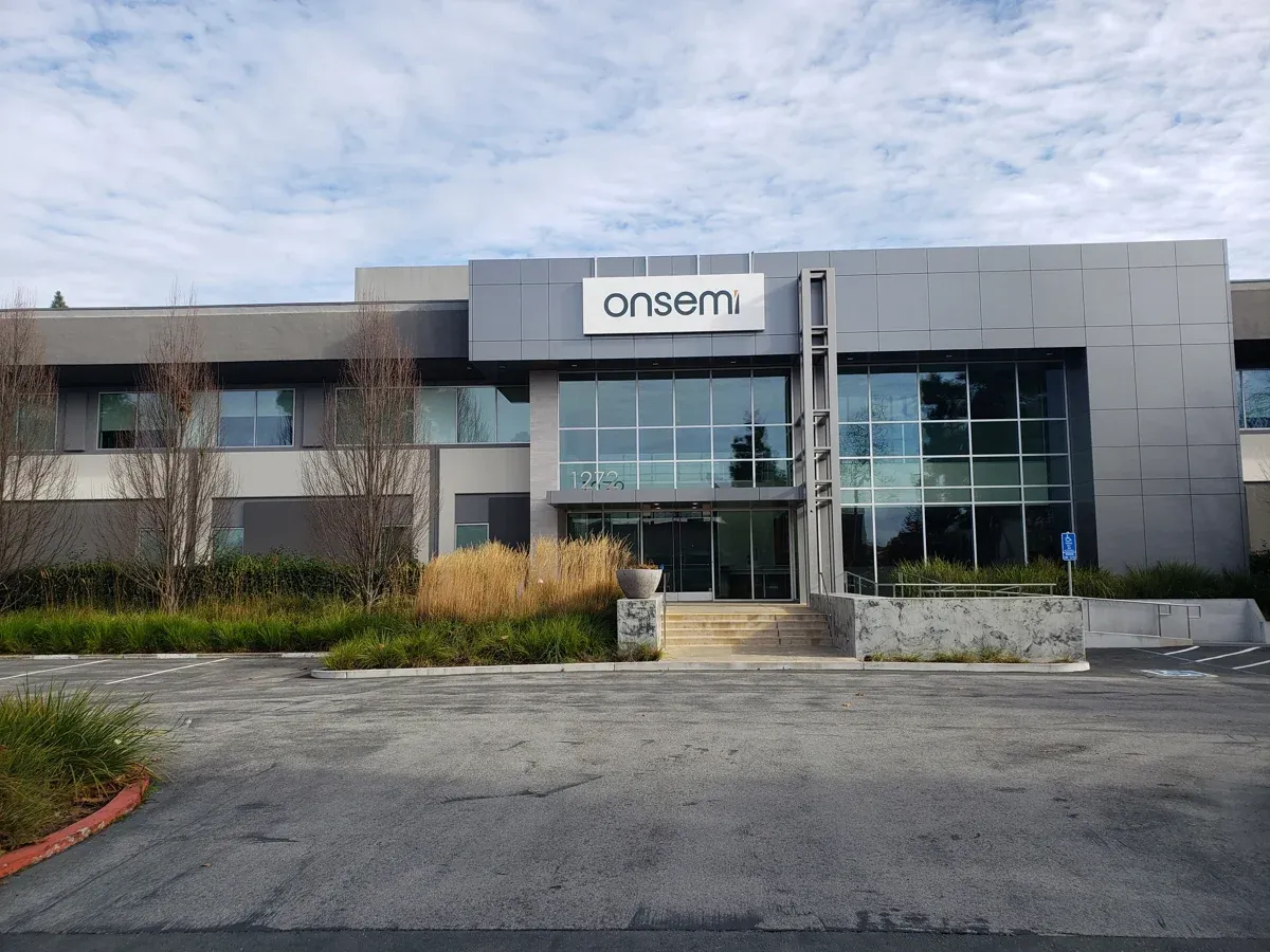
TL;DR At Investor Day, onsemi outlined a strategy spanning power and sensing across automotive, industrial and AI data centers. Its $213 billion estimate is a 2030 addressable-market opportunity, not company revenue guidance.
The strategy moves beyond components toward system-level design. High-voltage devices, Treo analog/digital capabilities and Embedded Power Platform address different layers of electrical, thermal and physical integration.
Rising compute demand increases power-conversion challenges, but reusable technology does not guarantee revenue growth. Design adoption, production conversion and customer system economics will test the thesis. Market opportunity is a forecast; results remain to be earned.
Sources · onsemi / GlobeNewswire (2026-09-16)
11 Rebellions and ai& plan Japan inference deployment

TL;DR Rebellions and ai& announced a RebelRack deployment partnership in Tokyo. An initial purchase is intended to scale toward roughly 100 or more racks; that is a target, not an installed count.
Catch-up on the September 15 announcement, not a new announcement today.
Rebellions joins ai&’s heterogeneous infrastructure to expand local inference options. The release does not disclose the initial rack count or the value of this specific transaction.
ai&’s more than $2 billion infrastructure capital and 40MW end-2027 target describe its broader buildout, not a Rebellions order or dedicated chip power allocation. Live service, supported models and measured latency, throughput and cost will determine value to users.
Sources · Rebellions (2026-09-15)
Silicon Market · 15
13 US listings use TradingView; two Korean listings use Naver links. Quotes are dynamic and may be delayed. Closing snapshots and ±3% mover research checks remain incomplete.
Allow external services in cookie settings to show the chart.
All 15 semiconductor stocks
Samsung Electronics · 005930 · Naver Finance
SK hynix · 000660 · Naver Finance
Frequently Asked Questions
What did Winbond agree to acquire from Infineon?
Winbond agreed to acquire 100% of Infineon's NOR Flash and F-RAM business in cash, at a $1.12 billion base price subject to adjustments. Closing is expected in the second half of 2027, subject to approvals and other conditions, and Winbond plans to revive the Spansion name.
What CHIPS R&D award did IBM's Anderon receive?
The US Commerce Department signed a final CHIPS R&D award of up to $1 billion for IBM subsidiary Anderon, supporting a 300mm quantum-wafer foundry. IBM describes a separate $1 billion company investment; the two are distinct funding sources, and the award ceiling is not proof that all funding has been disbursed.
What is new in MLPerf Inference 6.1?
MLPerf Inference 6.1 adds End-to-End RAG and Edge Agentic Inference tests, and thirty organizations submitted results. NVIDIA Rubin and Vera Rubin NVL72 submissions are Preview results, not equivalent to currently available systems.
Has SK hynix finalized a US memory wafer plan with Intel?
Reuters reported talks over producing SK hynix memory wafers in the US with Intel. SK hynix said it is exploring options but has finalized no specific plans or arrangements, so this is not a signed US fab contract or a confirmed HBM production plan.
What 2030 goals did China set for electronics manufacturing?
MIIT outlined 2030 goals including revenue above CNY30 trillion for enterprises above the designated size and R&D intensity of 3.5%. Neither figure is a chips-only target; the plan also covers components, materials, measurement equipment, photonics and AI hardware.
Related reading
- Daily Silicon: Intel-Apple Chip Deal Surges 10%, Samsung-SK Cap Gap…
- Daily Silicon: Intel 18A-P Risk Production, SK Hynix Nasdaq ADR, TSMC…
- Daily Silicon: AMD 2nm Defects to Samsung, SK hynix Tests Intel EMIB —…
- Daily Silicon: Analyst Consensus Surge vs TSMC April Slowdown,…
- TSMC Eyes Sixth Straight Record Profit; Intel, Qualcomm Hike CPU Prices…