VLSI Korea
Eliyan Deep Dive: NuLink's Standard-Package Chiplet Interconnect, the $1B Valuation, and the Arm Takeover Question
Eliyan sells the wires between chiplets: 64 Gbps per bump on standard organic packaging, a cap table spanning Intel, Samsung, SK hynix, AMD, Arm and Meta, a $1B Series C — and a reported $3B takeover question. The full deep dive.


The 30-Second Summary
- Eliyan sells the wires between chiplets. The Santa Clara startup's NuLink PHY moves data between dies at up to 64 Gbps per bump on ordinary organic package substrates — the cheap, plentiful kind — at bandwidth density and power levels the industry normally associates with silicon interposers. Its founder, Ramin Farjadrad, literally wrote one of the two open die-to-die standards (Bunch of Wires) his company now implements.
- The cap table is the strategy. Intel Capital and Micron Ventures anchored the 2022 Series A; Samsung Catalyst Fund and Tiger Global co-led the 2024 Series B with SK hynix participating; AMD, Arm, Coherent and Meta wrote a $50 million strategic check in January 2026; and a $145 million Series C in July 2026 — led by Seligman Ventures with Cisco Investments and Lumentum — put a $1 billion valuation on the company.
- In twelve months the product line escaped the package. NuLink-XD (July 2026) is a 224G PAM4 SerDes for chip-to-module links, and NuLight (October 2026) is a 2D microVCSEL optical chiplet platform aimed at rack-scale AI fabrics. Eliyan now claims a continuum from die-to-die to rack-to-rack.
- The open question is the exit. In October 2026, reporting revealed takeover interest, early talks with strategic investor Arm, at least one bid, and a banker hired to weigh options against a reported ~$3 billion target valuation — three times the July mark. No agreement exists. Revenue, meanwhile, was still in the low millions in 2025, with management forecasting hundreds of millions by the end of 2027.
The Company in One Table
| Item | Detail |
|---|---|
| Founded | 2021, Santa Clara, California (core interconnect technology in development since 2017, at Aquantia) |
| Founders | Ramin Farjadrad (CEO), Syrus Ziai, Patrick Soheili |
| Farjadrad background | Co-founded Aquantia, its chief engineer for ~15 years; after Marvell acquired Aquantia in 2019, CTO and VP of Marvell's networking and automotive division; inventor of the Bunch of Wires (BoW) interconnect adopted by the Open Compute Project |
| Ziai / Soheili background | Ziai: former Qualcomm engineering VP. Soheili: former VP of business development at eSilicon |
| Products | NuLink PHY IP (die-to-die), NuLink-XS (chip-to-chip), NuLink-XD (224G SerDes), NuGear chiplets, NuLight optical chiplets (Nexus, Oscar) |
| Process nodes | 5nm / 4nm / 3nm / 2nm, across four foundry partners (TSMC and Samsung Foundry publicly confirmed) |
| Disclosed funding | ~$295 million across four announced rounds (2022–2026) |
| Latest valuation | $1 billion (Series C, July 2026); ~$3 billion reported as a takeover target (October 2026, unconfirmed) |
| Patents | 100+ (company statements) |
| Revenue | Low millions of dollars in 2025 (executive statement); management forecast: hundreds of millions by end of 2027 |
Timeline: From Ethernet DNA to a Unicorn
| Date | Milestone |
|---|---|
| 2017 | Interconnect work begins inside Aquantia, Farjadrad's Ethernet PHY company |
| 2021 | Eliyan founded in Santa Clara |
| Nov 2022 | $40M Series A (Tracker Capital led; Celesta, Intel Capital, Micron Ventures, Cerberus) + first tapeout on TSMC 5nm announced together |
| 2023 | First silicon: 5nm NuLink at 40 Gbps/bump, 2.2 Tbps/mm beachfront at 130µm pitch on standard organic packaging; industry's first working silicon compliant with OCP's BoW 2.0 |
| Mar 2024 | $60M Series B co-led by Samsung Catalyst Fund and Tiger Global; Intel Capital, SK hynix, Cleveland Avenue, Mesh Ventures participate |
| Nov 2024 | NuLink taped out on Samsung Foundry SF4X 4nm (x64 UCIe advanced-package module; first silicon Q1 2025); custom HBM4 base-die program with Samsung ecosystem |
| 2025 | NuLink 2.0 on 3nm: 64 Gbps/bump. Joins Arm Total Design ecosystem (November) |
| Jan 2026 | $50M strategic round: AMD, Arm, Coherent, Meta, plus returning Samsung Catalyst Fund and Intel Capital |
| Q1 2026 | 224G devices begin sampling; management says first NuGear chiplet shipments begin during 2026 |
| Jul 24, 2026 | NuLink-XD unveiled: 224G PAM4 SerDes on TSMC 3nm for chip-to-chip and chip-to-module |
| Jul 29, 2026 | $145M Series C at $1B valuation (Seligman Ventures led; Cisco Investments, Lumentum join) |
| Oct 9, 2026 | Takeover interest reported: early talks with Arm, at least one bid received, investment bank hired; ~$3B target discussed |
| Oct 14, 2026 | NuLight unveiled at OCP Summit 2026: Nexus (1.6T reverse gearbox) and Oscar (electrical interface chip) 2D microVCSEL chiplets |
The Problem: Why Interposer-Class Bandwidth on a Plastic Substrate Is Hard
Every AI accelerator roadmap now runs into the same arithmetic. Compute dies are reticle-limited, so systems are assembled from chiplets — and the package becomes the computer. What the dies can exchange is capped by three physical quantities: how many bumps fit along a die edge (the "beachfront"), how fast each bump can signal across the package channel, and how many picojoules each bit costs.
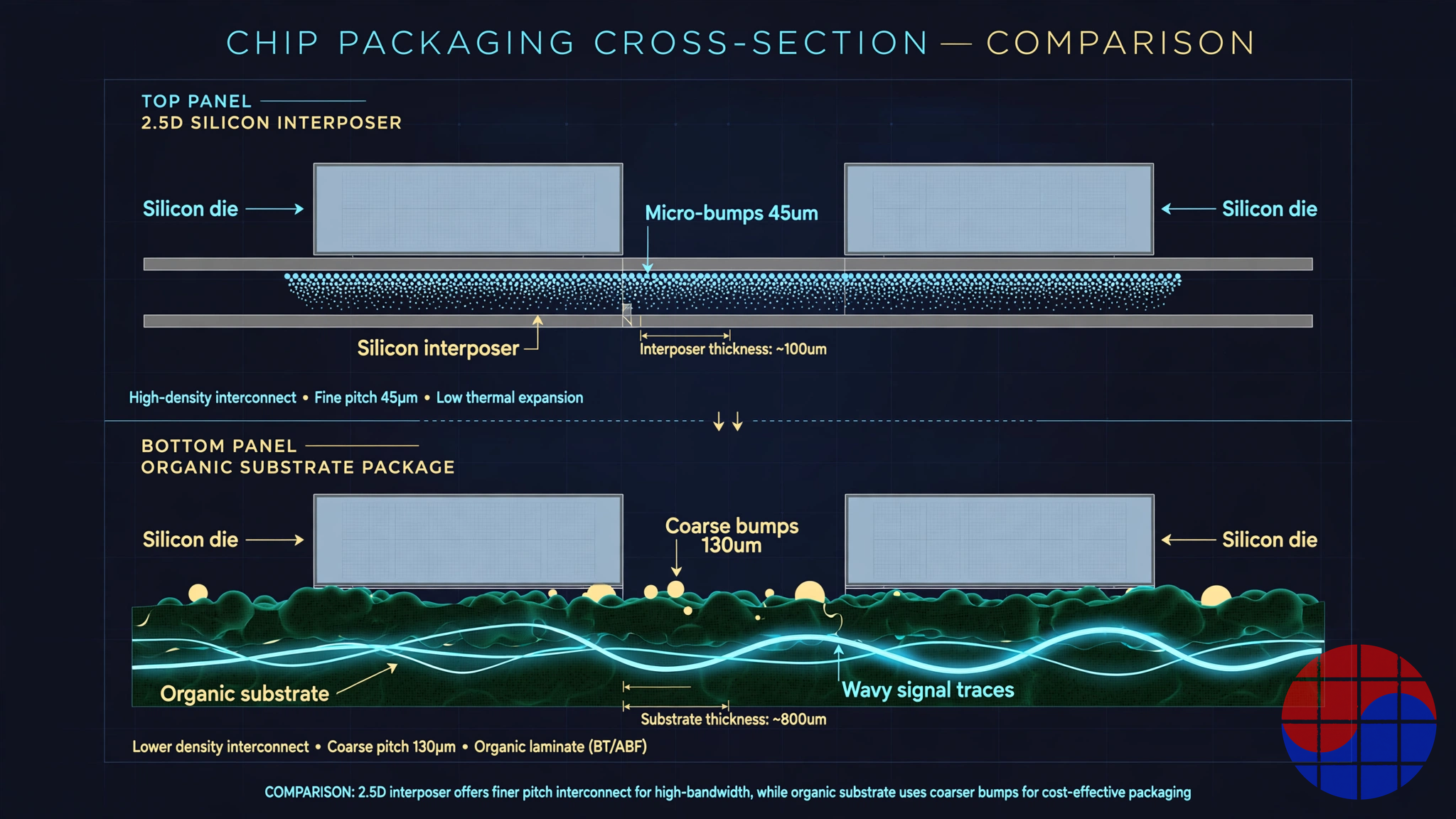
Silicon interposers — TSMC's CoWoS being the default — solve this by brute force: tens of thousands of micro-bumps at 40–55µm pitch on a silicon routing layer, with channels so short and clean that simple, low-power signaling works. The price is literal: interposer capacity is the industry's most contested resource, packages are size-limited and expensive, and lead times stretch. The mainstream UCIe specification reflects this split. UCIe defines two physical classes: UCIe-A (advanced package, reach up to ~2mm, fine micro-bump pitch) and UCIe-S (standard organic package, reach up to ~25mm at coarse C4 bump pitch). The standard-package class exists precisely because organic substrates are cheap and abundant — but its channel is electrically hostile: longer traces, rougher copper, more crosstalk, more loss. Through UCIe 2.0, per-pin rates topped out at 32 GT/s, and practical beachfront density on organic lagged interposer-class links by an order of magnitude. UCIe 3.0 raises the ceiling to 64 GT/s, at a power target of roughly 0.75 pJ/bit at top speed — on paper. Production-proven 64 GT/s PHYs on organic substrates are another matter.
Eliyan's founding bet is that the gap is a signal-processing problem, not a packaging-materials problem — and that a PHY smart enough can close most of it on the cheap substrate. That is an Ethernet PHY veteran's bet: Aquantia's business was squeezing 10-gigabit Ethernet through hostile copper cabling, using aggressive DSP and echo cancellation. NuLink applies the same philosophy inside the package.
NuLink Anatomy: Cancellation, Bidirectionality, and Protocol Agnosticism
Three design choices carry the whole architecture.
1. Interference cancellation as the core trick. NuLink's patents center on canceling the crosstalk and reflections that make organic-substrate channels unusable at high per-pin rates. The demonstrated result: NuLink 1.0 silicon in 5nm ran 40 Gbps per bump at a coarse 130µm bump pitch on a standard organic substrate, delivering over 2.2 Tbps/mm of beachfront bandwidth — and the company said the same PHY could reach ~3 Tbps/mm at finer standard-package pitches. NuLink 2.0 on 3nm pushed the per-bump rate to 64 Gbps, a figure independent coverage of the 3nm standard-package implementation puts at up to ~4.55 Tbps/mm of beachfront density.
2. Simultaneous bidirectional (SBD) signaling. Borrowed conceptually from full-duplex Ethernet, SBD transmits and receives on the same wire at the same time, separating the two directions by canceling the local echo. On a beachfront-starved die edge, sending both ways on one bump effectively doubles usable bandwidth per millimeter of die edge — without doubling the bumps. It is the single most "Aquantia" feature in the portfolio.
3. One PHY family, every open protocol. NuLink speaks UCIe and BoW natively, and adds two proprietary modes: UMI (Universal Memory Interface), a bidirectional scheme aimed at die-to-memory links and custom HBM base dies, and SBD. The PHY is licensed as IP for standard packages (NuLink-SP, bump pitch 100–130µm) and advanced packages (NuLink-AP, 40–55µm), and Eliyan also sells its own silicon: NuGear chiplets for memory expansion and scale-up networking (link bandwidths from 1.6T to 12.8T per device, per the company), plus the NuLight optical line.
The spec sheet (Eliyan's published product data)
Standard package (organic substrate, NuLink-SP):
| Mode | Data rate per lane | Beachfront BW | Area BW | Reach |
|---|---|---|---|---|
| UCIe unidirectional (baseline) | 32 Gbps | 1.8 Tbps/mm | 1.1 Tbps/mm² | 50 mm |
| NuLink UCIe | 64 Gbps | 3.6 Tbps/mm | 2.3 Tbps/mm² | 50 mm |
| NuLink BoW | 64 Gbps | 4.1 Tbps/mm | 3.1 Tbps/mm² | 50 mm |
| NuLink SBD (simultaneous bidirectional) | 64 Gbps (2×32) | 4.1 Tbps/mm | 3.1 Tbps/mm² | 5 mm |
Advanced package (silicon interposer / bridge, NuLink-AP):
| Mode | Data rate per lane | Beachfront BW | Area BW | Reach |
|---|---|---|---|---|
| UCIe unidirectional | 40 Gbps | 13.2 Tbps/mm | 9.1 Tbps/mm² | 2 mm |
| NuLink SBD | 64 Gbps (2×32) | 21.1 Tbps/mm | 14.6 Tbps/mm² | 2 mm |
NuLink vs. the UCIe specification
| Parameter | UCIe-S (spec, standard pkg) | UCIe-A (spec, advanced pkg) | Eliyan NuLink (shipping IP) |
|---|---|---|---|
| Package | Organic substrate, C4 bumps | Interposer/bridge, micro-bumps | Both classes, one PHY family |
| Max per-pin rate | 32 GT/s (≤2.0); 64 GT/s (3.0) | 32 GT/s (≤2.0); 64 GT/s (3.0) | 64 Gbps/bump in silicon (3nm, organic) |
| Channel reach | up to ~25 mm | up to ~2 mm | 50 mm (standard pkg, unidirectional modes) |
| Power target | <0.5 pJ/bit (lower rates); ~0.75 pJ/bit at 64 GT/s (3.0) | <0.5 pJ/bit class | Company claim: under 0.5 pJ/bit; ~30% of advanced-package solutions' power in early disclosures |
| Directionality | Unidirectional lanes | Unidirectional lanes | Unidirectional + simultaneous bidirectional (SBD) |
| Protocols | UCIe (PCIe/CXL/streaming) | UCIe | UCIe, BoW, UMI (proprietary), SBD |
Read the table the way a packaging engineer would. Eliyan does not beat the interposer at its own game — NuLink-AP's numbers exist to keep Eliyan IP inside advanced packages too. The disruption claim is narrower and more credible: on the substrate that costs a fraction as much and is not capacity-rationed, NuLink's 64 Gbps/bump and 50mm reach roughly double the practical envelope the UCIe-S class was designed around. The honest caveat is that the highest beachfront figures are configuration-dependent, and the 64 GT/s UCIe 3.0 specification means standards-based rivals are now designing to the same per-pin rate. Eliyan's durable edge, if any, is measured in characterized silicon across nodes and foundries — not in headline rates.
Beyond the Package: XS, XD, and the Optical Turn
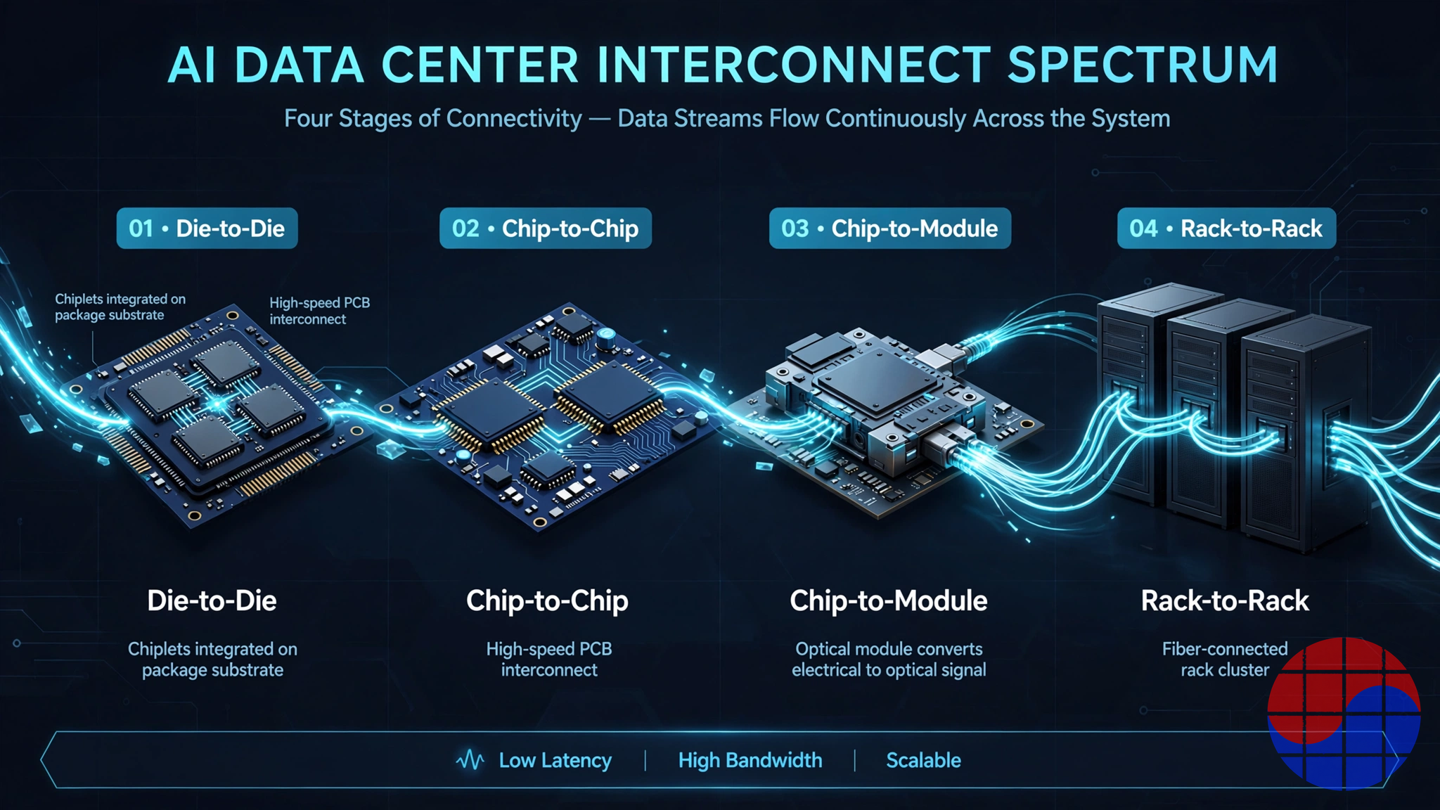
The 2026 product launches reframed Eliyan from a die-to-die IP vendor into a full-spectrum interconnect company:
- NuLink-XS extends the same low-power PHY philosophy chip-to-chip across a PCB: 32–40 Gbps per lane (XS 1.0) and 64 Gbps (XS 2.0) over 100mm of board reach, positioned against 112G/224G SerDes at much lower power.
- NuLink-XD (July 24, 2026) is the concession that the industry's center of gravity at the package edge is 224G PAM4: a TSMC 3nm SerDes for chip-to-chip and chip-to-module links, with a power-versus-reach configurable architecture claiming up to 40% lower power than comparable solutions, feeding near-package optics and OSFP/XPO modules.
- NuLight (October 14, 2026) is the optical bet: Nexus, a 1.6T reverse-gearbox chiplet, and Oscar, an electrical interface chip, driving 2D microVCSEL arrays. The architecture is deliberately "slow-and-wide" — many parallel NRZ optical lanes instead of a few fast PAM4 lanes — claiming 8× the bandwidth density, 5× the power efficiency and 50× the reach of copper, with an initial optical reach target around 50 meters and copper-like reliability. NuLight chiplets are sold to module makers for NPO/XPO optical modules.
The logic is consistent: wherever bits leave a die — to a neighboring die, a neighboring package, a module, or another rack — Eliyan wants its PHY (or its chiplet) in the path, under one "power per bit" story. It is also a hedge: if the industry's bandwidth frontier moves off-package faster than expected, Eliyan is not stranded inside the package.
The Money: Four Rounds, One Pattern
| Round | Date | Amount | Lead | Notable participants |
|---|---|---|---|---|
| Series A | Nov 2022 | $40M | Tracker Capital | Celesta Capital, Intel Capital, Micron Ventures, Cerberus |
| Series B | Mar 2024 | $60M | Samsung Catalyst Fund + Tiger Global (co-lead) | Intel Capital, SK hynix, Cleveland Avenue, Mesh Ventures |
| Strategic round | Jan 2026 | $50M | — (strategic investors) | AMD, Arm, Coherent, Meta; Samsung Catalyst Fund and Intel Capital returned |
| Series C | Jul 2026 | $145M | Seligman Ventures | Cisco Investments, Lumentum (new); Umesh Padval joined the board |
| Total disclosed | ~$295M | Valuation: $1B at Series C |
Notice what is missing: a single "natural" owner. The memory industry (Micron, Samsung, SK hynix — all three majors), the CPU/IP world (Intel, AMD, Arm), a hyperscaler (Meta), and now the networking/optics chain (Cisco, Lumentum, Coherent) each hold a piece. That breadth is Eliyan's sales channel and its shield — every strategic investor is a potential design-in — and it is also why a takeover is complicated: any acquirer buys a company partly owned by its competitors. The January 2026 round deserves emphasis: hyperscaler and platform money (Meta, AMD, Arm) arrived before the financial Series C repriced the company, and the Series C's new strategics (Cisco, Lumentum) map exactly onto the XD/NuLight optical pivot announced the same week.
Competition: Four Camps, One Chokepoint
The standards IP establishment. Cadence, Synopsys and Alphawave Semi sell UCIe PHY IP as part of broad interface portfolios. Their advantage is bundling and support infrastructure; their weakness is that die-to-die is one product line among hundreds. Eliyan's counter-pitch is focus: D2D PHY is the whole company, characterized across 5/4/3/2nm and multiple foundries, with proprietary SBD/UMI modes the standards do not offer.
The interposer camp. TSMC (CoWoS), Samsung and ASE sell the incumbent answer: pay for advanced packaging and the bandwidth problem mostly disappears. Eliyan does not fight this head-on — NuLink-AP licenses into advanced packages too — but its standard-package line is a direct tax on the camp's scarcity pricing. Every AI ASIC designed for organic substrate is a CoWoS slot someone else gets. The counter-risk is symmetrical: CoWoS capacity keeps expanding, and each expansion shrinks the premium on Eliyan's escape valve.
The proprietary platform owners. NVIDIA's NVLink (and its NVLink Fusion licensing program), Broadcom's scale-up Ethernet push and hyperscalers' in-house SerDes teams internalize the interconnect layer wherever volumes justify it. Eliyan's market is everyone else: the long tail of ASIC startups, second-tier hyperscaler programs, memory-adjacent devices and networking silicon that cannot justify a captive PHY team. That is a real market — but it caps Eliyan's ceiling at "arms dealer," not platform.
The optical camp. Ayar Labs is the benchmark: TeraPHY optical I/O chiplets, a $500 million Series E in March 2026 at a $3.75 billion valuation ($870 million raised in total), partnerships spanning NVIDIA, AMD and Alchip. Lightmatter (photonic interposer fabric), Celestial AI (photonic fabric for memory) and Avicena (microLED) crowd the same frontier. NuLight's microVCSEL slow-and-wide approach is Eliyan's differentiator — VCSELs are the cheapest, most manufacturable lasers in the industry — but Ayar has a multi-year head start in customer programs, and Eliyan's optical revenue is, so far, a product announcement rather than a shipment.
Eliyan's own framing, repeated by CEO Farjadrad in 2026, is that GPUs in AI clusters run at only 30–40% utilization because data cannot arrive fast enough — a vendor's number, but directionally the industry consensus, and the reason interconnect has become the most contested layer in AI infrastructure.
Adoption Reality Check
What is verifiable as of October 2026: silicon-proven PHYs at 5nm (first silicon 2023), 4nm (Samsung SF4X tapeout, November 2024) and 3nm (NuLink 2.0 at 64 Gbps/bump); ports across four foundries; an Arm Total Design partnership that puts NuLink in front of Arm-based ASIC programs; a Samsung Foundry relationship with an on-the-record endorsement from a Samsung EVP ("Eliyan's technology enables Samsung's customers to fully leverage its process technologies and memory products"); 224G devices sampling since Q1 2026; and management statements that NuGear chiplet shipments begin in 2026.
What is not public: a single named customer in production. Eliyan has never disclosed a design-win name, a production volume, or audited revenue. Management's own figures — 2025 revenue in the low millions, a forecast of hundreds of millions by the end of 2027 — describe a company whose valuation rests on design-ins still converting. This is normal for PHY IP at this stage (licensing revenue precedes royalties by years), but it means the $1 billion mark, and certainly the reported $3 billion takeover target, price the pipeline, not the P&L.
The quiet strategically Korean thread: custom HBM base dies. As HBM4 moves logic into the base die, the XPU-to-memory link becomes a designed interface rather than a fixed standard — exactly the socket UMI was built for, and the context of Eliyan's Samsung SF4X work and its disclosed alignment with emerging SPHBM4e memory interconnect work. With Samsung Catalyst and SK hynix both on the cap table, Eliyan is one of very few US startups wired into all three memory majors' roadmaps.
Risks
- Conversion risk. Design-ins are not revenue. If the 2026–2027 design-in wave slips a node generation, the hundreds-of-millions 2027 forecast — already an executive projection — slips with it.
- The standard is catching up. UCIe 3.0 specifies 64 GT/s. Eliyan's rate advantage is now a characterization-and-power advantage, which is harder to market and easier for EDA giants to close with bigger validation teams.
- Platform owners keep eating the layer. NVLink Fusion turns even NVIDIA's fabric into licensed IP; hyperscalers keep hiring SerDes teams. The independent-PHY market could narrow to the segment platform owners ignore.
- Advanced packaging deflation. Every CoWoS expansion and glass-substrate advance reduces the scarcity premium that makes organic-substrate heroics valuable.
- Optical execution. MicroVCSEL arrays at AI-fabric reliability and volume are unproven at Eliyan; Ayar Labs and silicon-photonics incumbents have years of qualification lead.
- Takeover overhang. A reported ~$3B ask against a $1B July mark and low-millions 2025 revenue invites a long negotiation; a failed process can chill the Series D that the optical expansion will need.
Chase's Take
I spend my days in signoff timing, so let me translate Eliyan's pitch into STA language: a die-to-die PHY is a timing-closure problem stretched across the worst channel in the system. On an interposer, the channel is so clean that closure is almost free. On organic substrate at 64 Gbps per bump, you are closing timing against loss, crosstalk and supply noise that move with temperature and process corner — which is why the winning technology is not a faster driver but a cancellation engine, and why it comes from a team that spent fifteen years doing echo cancellation for Ethernet. The Aquantia lineage is not biography; it is the product.
That also defines the real moat. Headline rates can be matched by any competent SerDes team with a spec sheet. What cannot be matched quickly is a library of characterized, silicon-correlated PHY macros across four foundries and four process nodes, with the failure modes already found. In PHY IP, the second tapeout on a new node is cheap; the first one is the company. Eliyan has been stacking first tapeouts since 2022.
On the takeover reports: interconnect IP gets valued on a spectrum between Arm (a platform royalty stream) and a SerDes team acqui-hire (a multiple of engineering payroll). Eliyan's cap table — three memory majors, both x86 rivals, Arm, Meta — makes it the rarest kind of asset: a neutral interconnect layer the whole industry has already paid to keep neutral. That neutrality is precisely what a single-owner acquisition destroys, and it is why the reported ~$3B number, if real, is a neutrality premium. My read: the bank process is as much about forcing the strategics to reveal their hands as about selling. If Arm does move, the logic would be Total Design completeness — owning the D2D PHY that every Arm-based chiplet ASIC needs — and the price of everyone else's neutrality will be the argument in the room.
For VLSI Korea readers, the actionable thread is HBM. Watch the custom base-die socket: if UMI-class PHYs land in HBM4-generation base dies through the Samsung ecosystem, Eliyan stops being a US IP story and becomes part of Korea's memory value chain — with Samsung Catalyst and SK hynix already inside the tent.
FAQ
Q: What does Eliyan actually sell — IP or chips? A: Both. NuLink, NuLink-XS and NuLink-XD are licensed PHY IP (customers integrate the macro into their own ASICs). NuGear and NuLight are Eliyan's own chiplets, sold as silicon for memory expansion, scale-up networking and optical modules.
Q: How is NuLink different from UCIe? A: UCIe is an open specification; NuLink is a PHY implementation family. NuLink implements UCIe (and OCP's BoW) protocols, then adds proprietary modes — SBD simultaneous bidirectional signaling and the UMI memory interface — and is specifically characterized to hit 64 Gbps per bump on standard organic substrates, where conventional UCIe-S implementations run at lower rates and shorter practical reach.
Q: Who has invested in Eliyan? A: Financial investors include Tracker Capital, Celesta, Tiger Global, Seligman Ventures and Cleveland Avenue. Strategic investors include Intel Capital, Micron Ventures, Samsung Catalyst Fund, SK hynix, AMD, Arm, Meta, Coherent, Cisco Investments and Lumentum — an unusually complete cross-section of the AI silicon industry.
Q: Is Eliyan making money? A: Not at scale yet, by its own account: executives put 2025 revenue in the low millions of dollars and forecast hundreds of millions by the end of 2027 as chiplet shipments begin (shipments were slated to start in 2026). Those are management statements, not audited figures; the company is private and does not publish financials.
Q: Is Arm acquiring Eliyan? A: No agreement has been announced. October 2026 reporting describes takeover interest, early talks with Arm (already a strategic investor via the January 2026 round), at least one bid from an undisclosed party, and an investment bank hired to evaluate options, with a target valuation around $3 billion discussed. Treat the $3 billion figure as an asking target, not a price.
Facts in this article were cross-checked against company announcements and independent reporting as of October 20, 2026. Figures described as company claims or executive statements are labeled as such; Eliyan is privately held and does not disclose audited financials. Related reading: our earlier chiplet startup map, Eliyan, Chipletz, and the startups turning the package into the system, and AI interconnect startups and the optical race.
📩 Subscribe to VLSI Korea
Get our daily semiconductor deep-dives delivered to your inbox first. Free to subscribe.