VLSI Korea
Google TPU v1 to Ironwood: Every Generation Compared (2026)
From TPU v1 to Ironwood, how compute, HBM, optical switching and compilers evolved into Google's integrated AI factory.


🆓 Free article · Anyone can read this article for free
This article is for readers comparing cloud AI accelerator architecture and system economics for purchasing, investment and supply-chain decisions. It separates peak specifications from model-level TCO and identifies the evidence that should validate the next generation.
Data cutoff: August 2, 2026
TL;DR
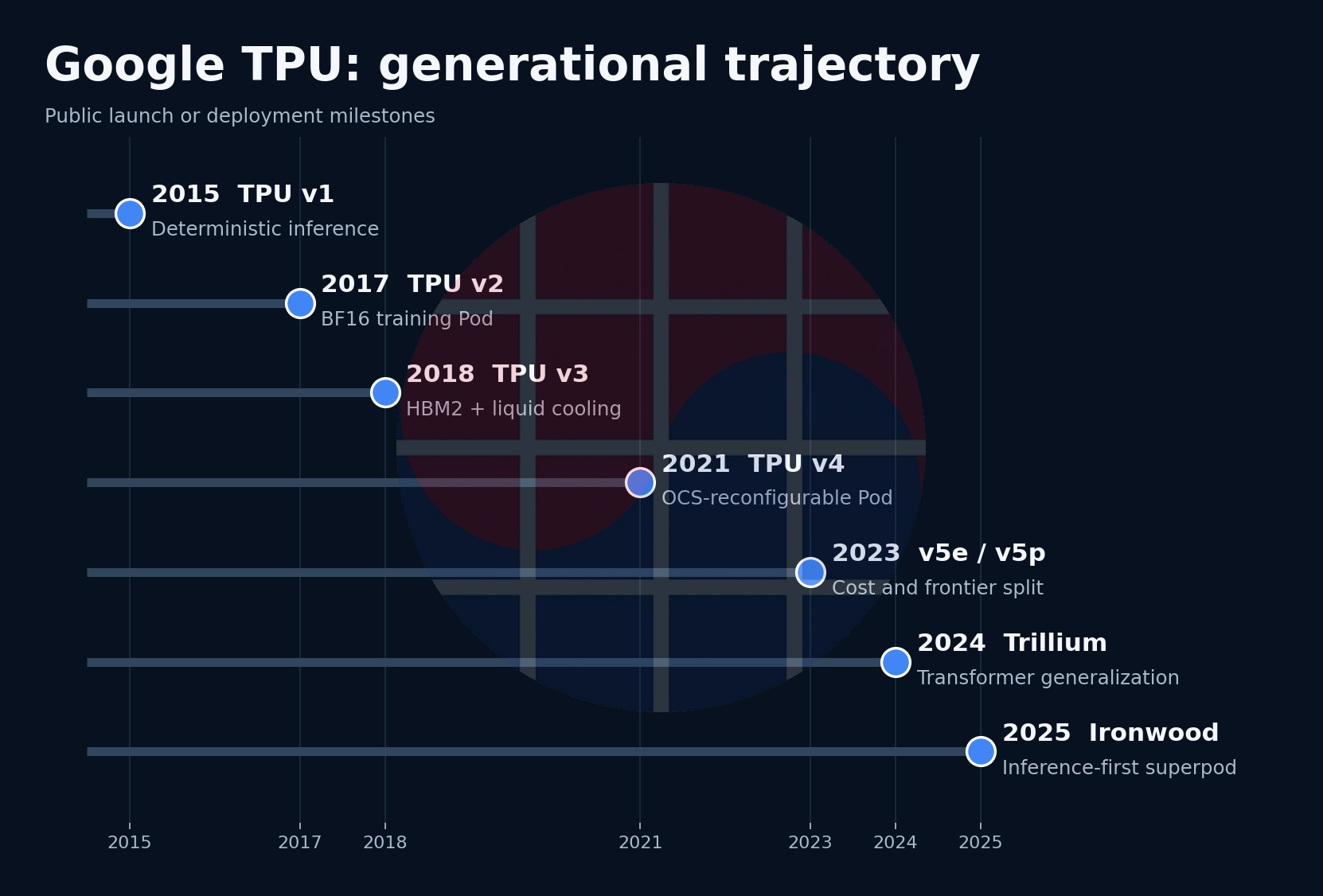
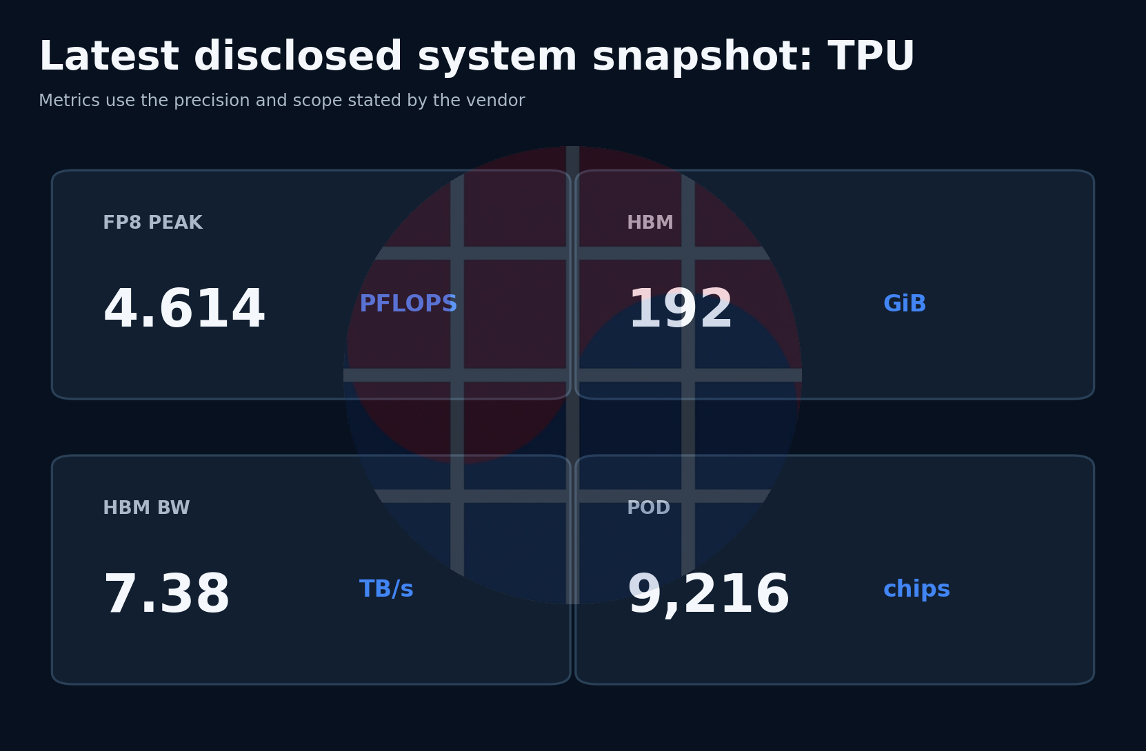
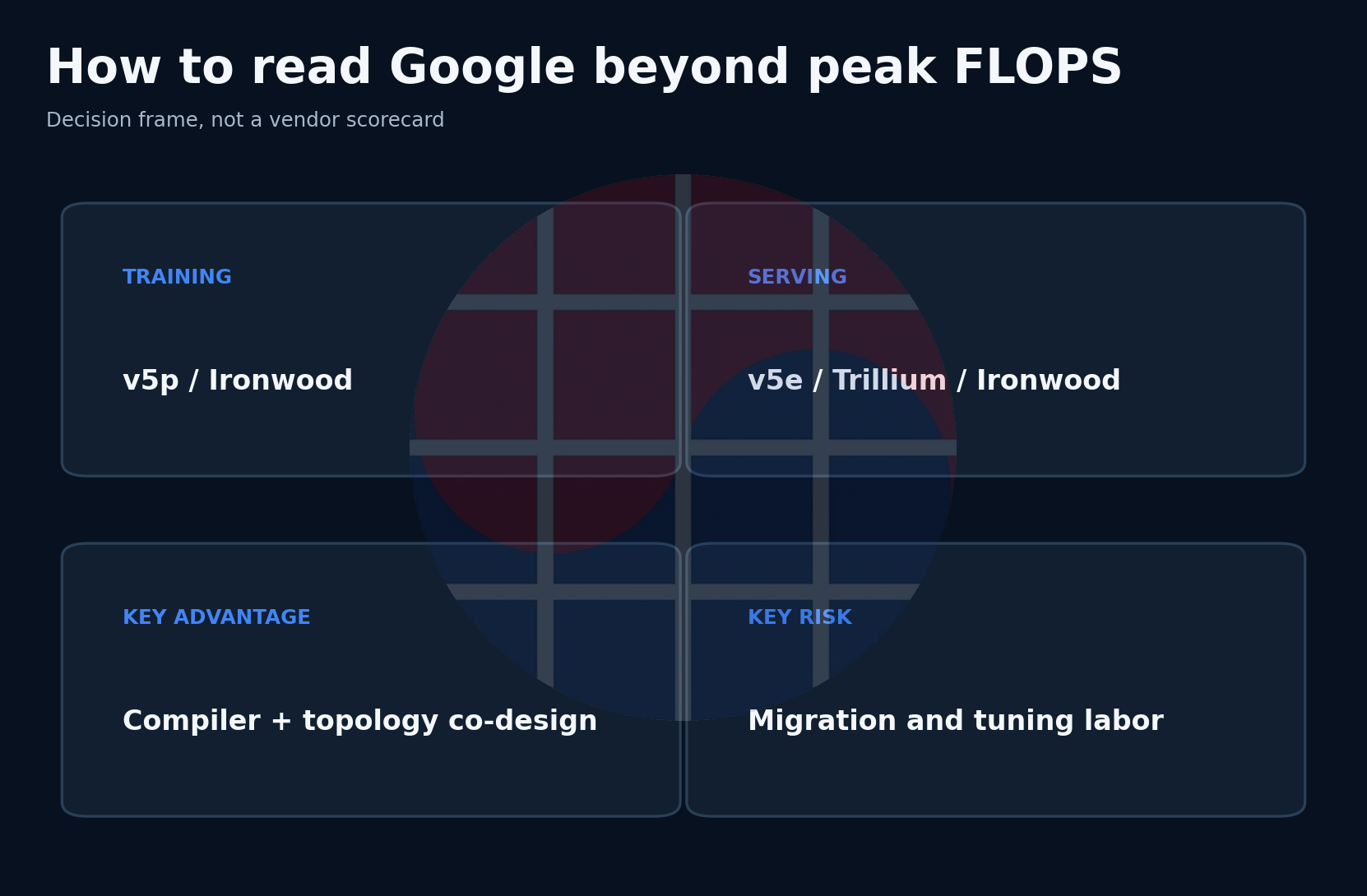
The defining feature of Google's TPU program is not the systolic array. TPU v1 was a deterministic datacenter ASIC built to control tail latency in search and speech inference. V2 and v3 added bfloat16, HBM and pod-scale interconnects, turning the TPU into a training platform. V4 used 4,096 chips and optical circuit switches to make the network a compiler-visible resource. V5e and v5p separated cost-efficient deployment from frontier training, while Trillium broadened Transformer coverage. Ironwood reunifies the design around a 9,216-chip system with 192 GiB HBM, 7.38 TB/s of memory bandwidth and 4.614 PFLOPS of FP8 peak compute per chip.
Google's moat is a decade of changing workload, model, compiler, network and fleet together. Its weakness is the other side of that same integration: CUDA assets are not directly portable, topology changes can require retuning, and an external Cloud TPU customer may not reproduce Google's internal operating efficiency.
Generation map
| Generation | Role | Peak per chip | Memory | System inflection |
|---|---|---|---|---|
| TPU v1 | Inference | 92 INT8 TOPS | 8 GiB DDR3, 28 MiB on-chip | Deterministic datacenter ASIC |
| TPU v2 | Training and inference | 45 BF16 TFLOPS | 16 GiB HBM | First Cloud TPU and 256-chip Pod |
| TPU v3 | Training and inference | 123 BF16 TFLOPS | 32 GiB HBM2, 900 GB/s | Liquid cooling and 1,024-chip Pod |
| TPU v4 | Large-scale training | 275 BF16 TFLOPS | 32 GiB HBM2, 1.2 TB/s | 4,096-chip optical reconfigurable Pod |
| TPU v5e | Cost-efficient train and serve | 197 BF16 TFLOPS | 16 GB, 800 GiB/s | 256-chip elastic 2D torus |
| TPU v5p | Frontier training | 459 BF16 TFLOPS | 95 GiB, 2.765 TB/s | Up to 6,144-chip single slice |
| TPU v6e | General train and serve | 918 BF16 TFLOPS | 32 GB, 1.638 TB/s | 256-chip Transformer-optimized Pod |
| TPU7x | Frontier train and serve | 2,307 BF16 / 4,614 FP8 TFLOPS | 192 GiB, 7.38 TB/s | 9,216-chip Ironwood Pod |
The table preserves Google's published GB and GiB units. Peaks at different numerical precision should not be divided into a simple generational performance ratio.
TPU v1: deterministic inference first
Google began the v1 design in 2013 and deployed it in 2015 as a PCIe accelerator. Its 256 by 256 matrix unit contained 65,536 eight-bit MACs, backed by 28 MiB of software-managed on-chip memory and delivering 92 TOPS. It targeted the MLP, CNN and LSTM inference workloads then responsible for most of Google's production neural-network demand.
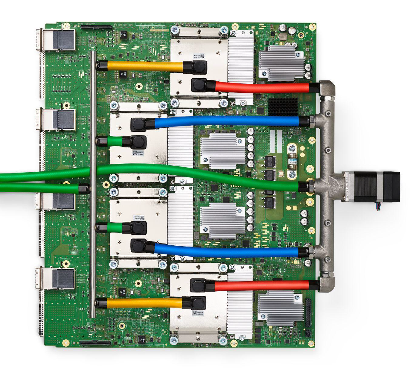
The key decision was to remove much of the machinery that improves average CPU performance, including out-of-order execution, speculative execution and an elaborate cache hierarchy. Search and speech cared more about predictable 99th-percentile latency. Giving the compiler and runtime more direct control made execution easier to bound even when the large MAC array was not perfectly utilized. Google's published gains of 15 to 30 times performance and 30 to 80 times TOPS per watt applied to its contemporary internal workloads, not to modern GPUs.
The bottleneck was equally instructive. Eight GiB of DDR3 and weak external bandwidth left low-arithmetic-intensity models unable to feed the array. Every later TPU generation therefore scaled memory and interconnect along with matrix compute.
TPU v2 and v3: from inference ASIC to training Pod
TPU v2 added bfloat16 training, HBM and a 256-chip pod. Bfloat16 retained FP32's eight-bit exponent while shortening the mantissa, preserving dynamic range while reducing multiplier area and data movement. The unit of design was no longer one chip but the pod.
V3 increased the chip to 123 BF16 TFLOPS and 32 GiB of HBM2 at 900 GB/s, then scaled to 1,024 chips. Roughly 220 W of average chip power pushed the system into liquid cooling. The important transition was not simply more compute. V3 could keep larger models, activations and batches in HBM while running data- and model-parallel collectives across the torus.
XLA became part of the architecture. It had to fuse operations, choose tensor layouts, shard graphs and insert collectives, not merely translate a TensorFlow program into instructions. Determinism is an advantage when the compiler finds a strong schedule; unsupported operations, dynamic shapes and host fallbacks turn it into friction.
TPU v4: an optical system advantage
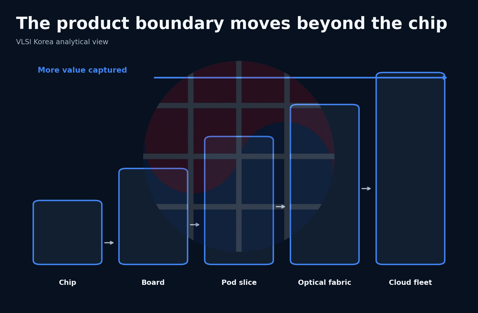
V4 provided 275 BF16 or INT8 TFLOPS, 32 GiB of HBM2 at 1.2 TB/s and a measured average power near 170 W per chip. Its 4,096-chip pod reached a nominal 1.1 EFLOPS, 1.1 PB/s of all-reduce bandwidth and 24 TB/s of bisection bandwidth.
The system innovation was a MEMS optical circuit switch. Instead of freezing the topology in electrical packet switches, Google could reconfigure long-lived optical paths, bypass failed chips and links, and carve slices matched to job size. Regular collective traffic is well suited to circuit switching. A twisted torus shortened wraparound cabling, while the compiler mapped logical topology onto the physical slice.
This made scheduling yield as important as silicon yield. A pod must remain useful when some of its 4,096 chips or links fail. V4 also established SparseCore as a system feature for embedding-heavy recommendation workloads, where lookup, gather and reduction can dominate dense GEMM.
TPU v5: economics split into v5e and v5p
V5e targeted elastic training and serving: 197 BF16 TFLOPS, 16 GB of HBM at 800 GiB/s, 400 GB/s bidirectional ICI and a 256-chip two-dimensional torus. Smaller slices improved provisioning and fleet utilization.
V5p targeted frontier training: 459 BF16 TFLOPS, 95 GiB of HBM at 2.765 TB/s, 1.2 TB/s ICI and four SparseCores. A pod contained 8,960 chips, with a single slice up to 6,144 and multislice configurations up to 18,432. Relative to v5e, its HBM capacity increased much faster than compute, allowing model state, activations and optimizer data to reside on fewer chips and reducing communication.
This is cloud economics expressed in silicon balance. Fine-tuning and inference value low hourly cost, small slices and quick provisioning. Frontier pretraining values large memory, high ICI and shorter wall-clock time. A common compiler surface lets Google vary those balances while keeping the fleet busy.
Trillium and Ironwood: larger tiles, then a memory-heavy AI system
Trillium retained a 256-chip pod while raising each chip to 918 BF16 TFLOPS or 1,836 INT8 TOPS. It doubled HBM capacity to 32 GB and raised bandwidth to 1.638 TB/s, with 800 GB/s bidirectional ICI. A larger 256 by 256 MXU and higher clock increased peak compute, but also required fusion and layout work to feed the array on small or irregular operations.
Ironwood shifts the balance again. TPU7x contains two TensorCores, four SparseCores, 192 GiB of HBM at 7.38 TB/s and 1.2 TB/s bidirectional ICI. Peak compute is 2.307 PFLOPS at BF16 and 4.614 PFLOPS at FP8. A pod contains 9,216 chips. Compared with Trillium, BF16 compute rises about 2.5 times, HBM capacity six times and bandwidth 4.5 times, while ICI rises only 1.5 times.
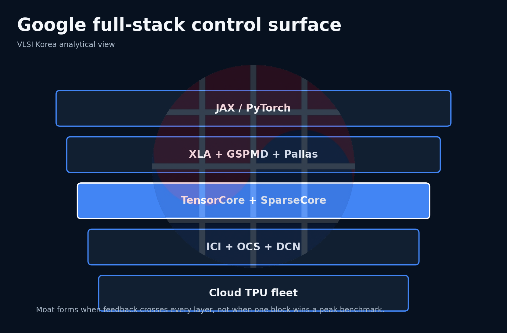
That ratio reveals the workload. Decode streams weights and KV cache, and large models benefit from greater residency. Because interconnect did not scale at the same rate, locality and sharding quality matter more. Google's ICI, optical switching and datacenter network provide the physical hierarchy; XLA, JAX, PyTorch/XLA and Pallas expose it to software.
Google calls Ironwood an inference-era chip, but the official product targets training, reinforcement learning and serving. “Inference first” is therefore an economic statement about token throughput and responsiveness, not a claim that the device is a single-purpose inference ASIC. TPU7x supports JAX and PyTorch but not TensorFlow, an important signal that hardware differentiation now depends on meeting developers at the industry's active software interfaces.
The real moat, and its cost
Production workloads from Search, YouTube, Gemini, Veo, Imagen and external frontier-model users provide rapid counterexamples for hardware design. XLA and GSPMD lower a model into both device kernels and multi-device sharding. Google also controls optical topology, datacenter networking and the Cloud TPU sales channel.
The moat creates lock-in. CUDA kernels do not execute unchanged. Customers must learn XLA compilation and sharding, and Google notes that topology and chip-count changes between generations may require significant tuning. Peak FLOPS are irrelevant when a custom operation falls back to the host, compilation dominates iteration, or the input pipeline and small-batch latency become the bottleneck.
Watch points
- Whether Ironwood FP8 training preserves convergence and reduces end-to-end time versus BF16.
- Whether model-parallel efficiency survives when HBM and compute grow much faster than per-chip ICI.
- Whether PyTorch/XLA and Pallas materially lower the migration cost of CUDA and Triton assets.
- How Google divides v5p and Ironwood capacity among frontier training, reinforcement learning and high-volume serving.
- Whether optical fault rerouting improves scheduling yield and long-running job availability at pod scale.
Contrarian read
TPU's strength could become a weakness if model architectures change faster than Google's compiler-and-silicon loop. Sparse MoE, state-space models, multimodal preprocessing and agent runtimes raise the share of work outside regular matrix multiplication. Vector units, SparseCore and Pallas help, but GPU SIMT flexibility and CUDA may absorb new operators faster.
The customer boundary is the second risk. Google's internal teams can work close to hardware and compiler engineers. An external customer may not have the same optimization loop. Even a superior published peak cannot win if usable model coverage, reservation availability and migration labor make the delivered cost higher than a GPU alternative.
Korean lens
For Korea's supply chain, the TPU story is larger than HBM demand. Each generation increases HBM capacity and bandwidth together with advanced packaging, optical connectivity, liquid cooling and power delivery. In a 9,216-chip Ironwood pod, qualified output of HBM stacks, substrates, optical modules, switches and rack infrastructure can limit deployment before accelerator die supply does.
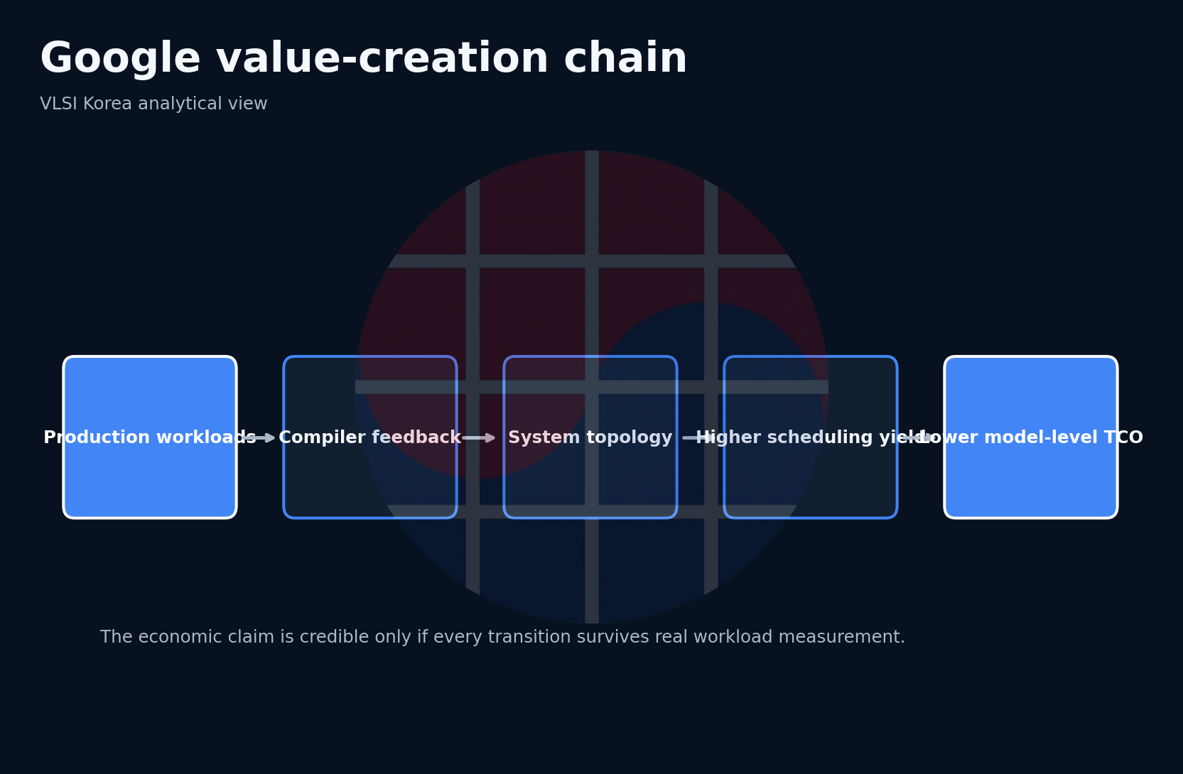
For Korean NPU startups, the transferable lesson is generational continuity. Compiler IR, kernel libraries, observability and collective communication must survive the transition to the next chip. Only then can an ASIC's lower hardware cost become lower model-level total cost.
Sources
- In-Datacenter Performance Analysis of a Tensor Processing Unit
- Cloud TPU architecture
- TPU v3 specifications
- TPU v4 specifications
- TPU v5e specifications
- TPU v5p specifications
- Introducing Trillium
- TPU v6e specifications
- TPU7x Ironwood specifications
- Training large models on Ironwood
Disclosure
This article is for informational purposes only and does not constitute a recommendation to buy or sell any security. Figures and facts are based on publicly available corporate disclosures, media reports and market research, and errors may occur in the source material or writing process. The author may hold shares of companies mentioned. Readers are solely responsible for all investment decisions and outcomes.