VLSI Korea
HBM's Hidden Bottleneck Is Test: The Inspection Wall Behind 16-High Stacks
The HBM race's real bottleneck is not bonding - it is test. Stack yield is a multiplication problem: 99% die yield becomes 88.6% at 12-high. How HBM4's 2,048-bit, 16-high era makes inspection time the constraint.


HBM's Hidden Bottleneck Is Test: The Inspection Wall Behind 16-High Stacks
30-Second Summary
The real bottleneck in the HBM race is not bonding — it is test. The HBM4 standard (JEDEC JESD270-4, finalized April 16, 2025) doubles the interface to 2,048 bits, expands independent channels to 32, and scales stacks to as high as 16-high and 512Gb (64GB). The arithmetic is unforgiving: even at a 99% per-die yield, a 12-high stack yields only about 88.6%, and at 95% per-die yield the stack yield falls to roughly 54%. Because one bad die condemns an entire stack, Known-Good-Die screening before stacking and full inspection after stacking are not quality options — they are the process that sets cost and lead time. The tester market confirms it in numbers. Advantest raised its 2026 tester market outlook to USD 13–14.5 billion in its July 2026 earnings release, and Teradyne's memory test revenue hit a record USD 212 million in Q2 2026. Korea's test ecosystem — Techwing, YC, ISC and Leeno — is already posting the results.
Background: Mass production has started, and all eyes are on bonding
The HBM4 production clock is already running. SK hynix completed its HBM4 mass-production system in September 2025 and, at its Q2 2026 earnings release, said mass supply began in the second quarter with production expanding in the second half. Samsung Electronics announced on February 12, 2026 that it had started HBM4 mass production and shipped commercial product — an industry first, in the company's own words. Samsung's HBM4 pairs a 1c (sixth-generation 10nm-class) DRAM with a 4nm logic base die, delivers a stable transfer rate of 11.7 Gb/s (46% above the JEDEC baseline of 8 Gb/s) and up to 13 Gb/s, and the company guided HBM revenue to more than triple year over year in 2026 (Samsung official release, February 12, 2026). Both makers have telegraphed the next steps: SK hynix completed HBM4E sample shipments in the first half of 2026, Samsung plans HBM4E samples in the second half, and full HBM4E production plus custom HBM samples are targeted for 2027.
Market attention, however, is fixed on one place: the TC bonder that stacks the dies. Hanmi Semiconductor is the emblem. In June 2026 it signed a KRW 44.2 billion supply contract with SK hynix for HBM4 TC bonders (4.5 GRIFFIN), and in Q2 2026 it posted revenue of KRW 251.1 billion (+39.5% YoY) and operating profit of KRW 130.3 billion (+51.0% YoY). It is undeniably critical equipment. But one distinction must be kept sharp: a TC bonder is bonding (stacking) equipment, not test equipment. No matter how fast dies are stacked, shipments do not grow unless test capacity can judge whether those stacks are good. In the HBM4 generation, what is actually getting tight is not stacking speed — it is inspection time.
Deep Dive 1: Yield multiplies downward — the inspection wall that 16-high builds
The reason test becomes the bottleneck is arithmetic. Stack yield is the product of die yields. Running the formula cited in industry explainers gives the following (author's calculation, by assumed per-die yield):
| Per-die yield | 12-high stack yield | 16-high stack yield |
|---|---|---|
| 99% | ~88.6% | ~85.1% |
| 97% | ~69.4% | ~61.4% |
| 95% | ~54.0% | ~44.0% |
A 95% die yield is by no means a poor figure for a DRAM process. Yet stack 16 of those dies and more than half the output is defective. A single GPU package carries eight HBM stacks, so a stack failure discovered after packaging destroys the entire high-value accelerator package. That is why "stack first, test at the end" cannot work for HBM. Wafer test certifying each die as a Known-Good-Die before stacking, and Known-Good-Stack test after stacking — accessible only through the base die — are structurally mandatory.
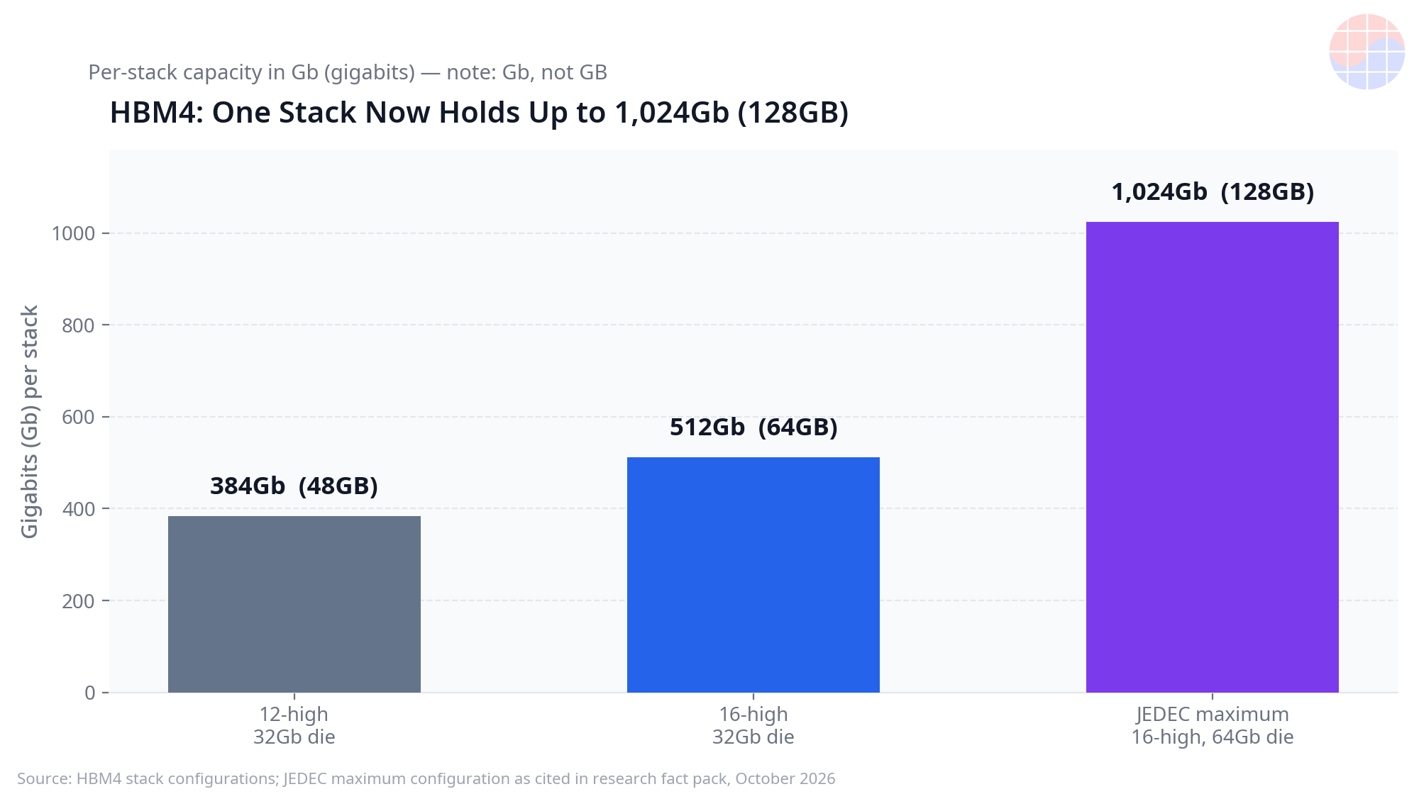
HBM4 makes the structure harsher. Under JEDEC JESD270-4 (April 16, 2025), stack heights are 4, 8, 12 and 16-high, with die densities of 24Gb or 32Gb. Sixteen 32Gb dies make a 512Gb (64GB) stack; twelve 24Gb dies make 288Gb (36GB); twelve 32Gb dies make 384Gb (48GB). The interface is 2,048 bits per stack, double HBM3's 1,024 bits, and independent channels doubled from 16 to 32, each with two pseudo-channels. Industry explainers put an HBM4 stack's connections at more than 20,000 TSVs and roughly 16,148 microbumps (figures from a single explainer source — estimates, not confirmed specifications). More connection points mean more junctions and more test items to inspect. With the voltage specification also subdivided (VDDQ 0.7–0.9V, VDDC 1.0V or 1.05V), test must run longer, under more conditions.
Deep Dive 2: Test shifts left — and the tester market is at record highs
The industry's response is to move test earlier — a "shift-left." The current standard flow, as tester and prober executives described it in industry technical media in 2026, has three stages. First, at wafer level, the internal circuits, core memory and TSVs of both the DRAM dies and the logic base die are tested, and wafer-level burn-in screens out early failures to secure KGDs. Second, after stacking, the whole stack is tested through the base die (KGS). Third comes final package test. As test moves from back-end toward front-end, these executives note, demand grows for high-speed test, parallelism and thermal control.
This is where the bottleneck takes shape. Burn-in cannot be compressed: it applies prolonged thermal and voltage stress to expose infant mortality, so as stack heights and test items grow, so does its duration. Meanwhile, a 2,048-bit interface with 32 channels inflates the tester resources needed per device, eroding how many devices one tester can handle at once — test parallelism. Unless equipment counts rise, inspection capacity cannot keep up with production capacity.
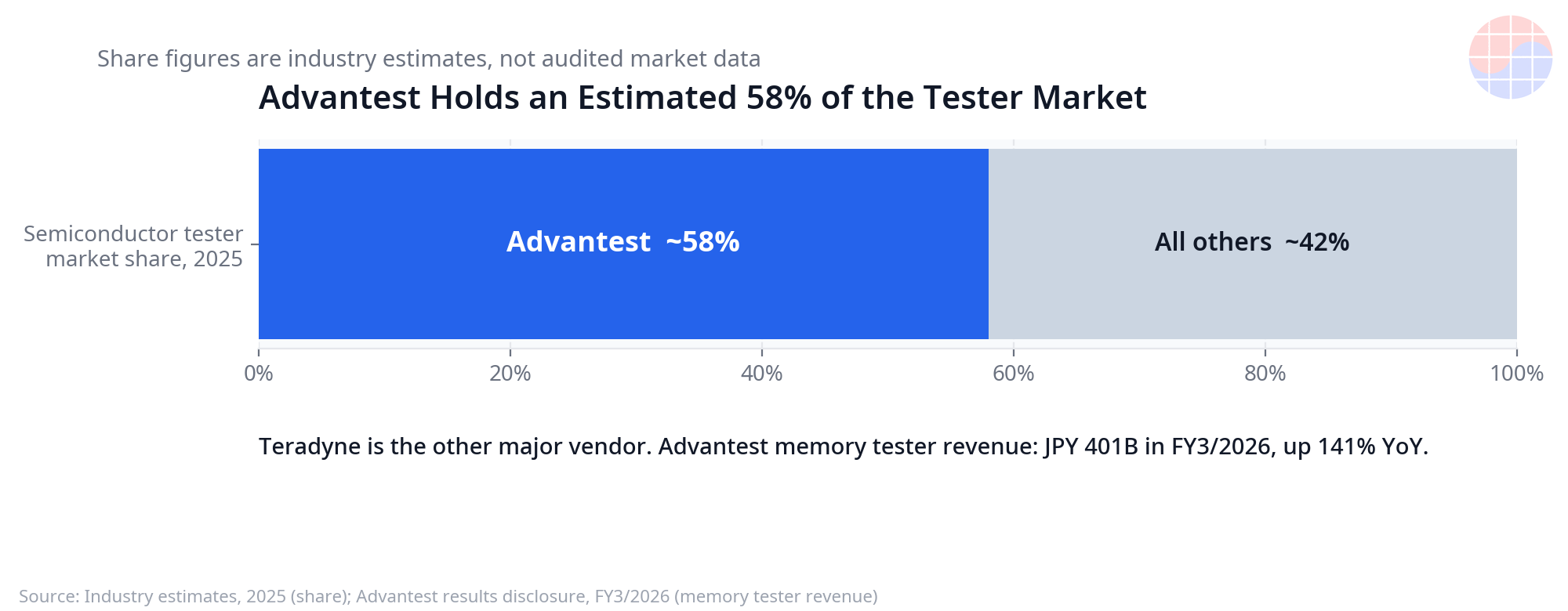
The market numbers back this up. Advantest's FY2026 first quarter (ended June 30, 2026; reported July 2026) delivered revenue of JPY 367.5 billion (+39% YoY) and operating profit of JPY 189.3 billion (+53% YoY). By segment, SoC testers brought in JPY 259.6 billion (+36% YoY) and memory testers JPY 48 billion (+43% YoY), with the company explicitly crediting tester sales for HBM, high-performance DRAM and NAND for memory tester growth. Advantest raised its 2026 tester market outlook to USD 13–14.5 billion in total, with memory testers at USD 2.5–3.0 billion — about 19% above its April outlook. Teradyne tells the same story. In Q2 2026 (reported July 2026), total revenue was USD 1.33 billion (+103.9% YoY), and within semiconductor test revenue of USD 1.12 billion, memory test reached a record USD 212 million, exceeding USD 200 million for a third consecutive quarter. Management cited HBM and DRAM test demand, noted a memory book-to-bill above 2, and projected the 2026 memory test market to be more than 40% larger than in 2025. When both tester leaders print record numbers simultaneously, test is no longer an appendage of the back-end.
Deep Dive 3: Korea's test ecosystem — the opening in equipment, sockets and pins
This bottleneck is arriving in Korea's test ecosystem in the form of earnings.
- Techwing (dedicated HBM inspection equipment): The core product is the Cube Prober, an inspection tool dedicated to HBM. Revenue in Q1 2026 was KRW 52.4 billion (+51.4% YoY), and preliminary Q3 2026 results were reported as revenue of KRW 87.8 billion (+110.2% YoY) and operating profit of KRW 18.0 billion (+153% YoY) (reported October 14, 2026; preliminary figures). In 2025, by contrast, HBM4 yield problems pushed Cube Prober adoption into the second half and operating profit fell to KRW 16.4 billion (-29.6%) — test equipment revenue itself is geared to customers' HBM4 ramp and yield schedules.
- YC (wafer testers): YC supplies wafer testers that inspect memory performance and defects. Consolidated Q2 2026 revenue was about KRW 105 billion (+31% YoY) and operating profit about KRW 15.1 billion (+249% YoY, a margin of roughly 14%). A supply contract was also disclosed in August 2026, though quarterly revenue recognition swings with customer capex and inspection schedules.
- ISC (test sockets): Q2 2026 revenue was KRW 72.9 billion (+41% YoY) and operating profit KRW 21.3 billion (+55% YoY, 29% margin), with AI-related revenue of KRW 59.1 billion (+71% YoY) taking 81% of the total (per the company's July 27, 2026 earnings materials). First-half cumulative revenue was KRW 141.2 billion with operating profit of KRW 44.9 billion. The mix deserves attention: 78% non-memory versus 22% memory, meaning the center of gravity sits not in direct HBM sales but in final-test and system-level test (SLT) sockets for AI accelerators and server CPUs.
- Leeno Industrial (test pins and sockets — consumables): Sockets and pins wear out with every inspection, so replacement demand follows test volume itself. First-half 2026 revenue was KRW 243.0 billion (+27.2% YoY) with operating profit of KRW 120.8 billion (49.7%); Q2 alone delivered revenue of KRW 143.2 billion and operating profit of KRW 73.5 billion (51.3%). IC test sockets rose from 57.2% of revenue in 2022 to 68.5% in the first half of 2026, and socket production grew from 130,672 units in 2024 to 191,102 in 2025 (+46%) (per a compilation posted September 25, 2026).
The picture, in sum: equipment that performs full inspection (Techwing, YC) sits on the direct benefit line of the HBM capex cycle, while parts consumed every time inspection repeats (ISC, Leeno) ride test volume. Hanmi's TC bonder does not belong in this picture — it is bonding equipment that shares customers and a cycle with the test ecosystem, nothing more.
Chase's Take: Test has moved from quality gate to capacity gate
For most of semiconductor history, test was a cost center that filtered defects, hiding behind bonder counts and lithography capacity in investment debates. In the HBM4 generation that status inverts: under multiplicative yield math, test capacity is shipment capacity. A stack that has not passed inspection is capacity that does not exist.
The closest analogy sits on the design side: signoff. However fast a chip is implemented, if it cannot clear timing signoff, the tape-out schedule stops on the spot. HBM test is moving into exactly that position. If a bonding line stacks 100,000 stacks a month but burn-in and KGS capacity cover only 80,000, real shipments are 80,000. The rest is inventory — and lead time.
From a Korean vantage point, the more interesting question is the form of the benefit. Equipment — Cube Probers, wafer testers — is a high-variance bet on a customer's ramp schedule. Sockets and pins are different. As consumables worn down as long as test volume exists, they behave less like a directional cycle bet and more like recurring revenue geared to volume. Leeno's operating margin hovering near 50% and ISC's 81% AI revenue share are what that structure looks like in numbers. The weaknesses are equally clear. As Techwing's 2025 downturn shows, Korean test equipment earnings are tightly bound to a handful of customers' HBM4 yield and production schedules. Whoever profits from a bottleneck is also exposed to how that bottleneck gets resolved.
Implications
- Memory capex allocation is shifting: As HBM4 production ramps in the second half of 2026, testers, probers and burn-in capacity will claim a larger share of memory makers' investment decisions. Advantest raising its memory tester outlook by roughly 19% within a single quarter is an early signal of that reallocation.
- Lead time is now set elsewhere: Judging HBM supply lead times by bonder deliveries alone is no longer sufficient. Inspection capacity — wafer-level burn-in and KGS test above all — determines actual shipment speed. Teradyne's memory book-to-bill above 2 means orders are running at more than double shipments.
- A re-rating window for Korea's supply chain: Techwing and YC are geared directly to HBM; ISC and Leeno are geared to AI test volume. Two distinct growth engines now coexist inside Korea's test ecosystem. Caveats travel with the numbers — preliminary results (Techwing's Q3) and lumpy quarterly revenue recognition (YC) need to be read alongside the growth rates.
- The next generation is harsher still: With full HBM4E production targeted for 2027 and custom HBM samples planned for 2027, base dies carry more logic and test items multiply further. The test bottleneck is not a one-generation phenomenon of HBM4; it is a structural variable that intensifies every generation.
FAQ
Q1. Why does test become the bottleneck in HBM? Because stack yield is the product of die yields. Even at 99% per-die yield, a 12-high stack yields only about 88.6%; at 95%, it falls to roughly 54%. One bad die can condemn an entire stack — and, with eight stacks per GPU package, potentially the whole package — so KGD screening before stacking and full inspection after stacking are mandatory, and that inspection time sets the shipment rate.
Q2. What is the difference between KGD and KGS test? KGD (Known-Good-Die) test verifies, at wafer level and before stacking, that each individual die is good, using wafer-level burn-in to remove early failures. KGS (Known-Good-Stack) test runs after stacking and tests the whole stack through the base die. Because an HBM4 stack's interior is reachable only through the base die, both stages are required.
Q3. Is Hanmi Semiconductor's TC bonder also test equipment? No. A TC (thermo-compression) bonder is bonding (stacking) equipment that attaches dies — not test equipment. Hanmi's Q2 2026 revenue of KRW 251.1 billion and its KRW 44.2 billion HBM4 TC bonder supply contract with SK hynix (June 2026) signal expanding bonding capacity, not test capacity. The two equipment families ride the same HBM investment cycle, but their functions must be kept separate.
Q4. Which Korean companies benefit directly from HBM test? In equipment, Techwing (the Cube Prober, dedicated HBM inspection equipment) and YC (memory wafer testers) are geared directly to HBM. ISC and Leeno center on consumables such as test sockets and pins — and in ISC's case, 78% of Q2 2026 revenue was non-memory, driven more by final-test demand for AI accelerators and server CPUs. Direct exposure and volume-linked exposure should be evaluated separately.
Note: Some figures in this article, including market outlooks and the yield formula, are drawn from industry explainers and company earnings releases; figures that are preliminary or otherwise unconfirmed are flagged as such in the text. Nothing here is a recommendation to buy or sell any security.
Sources
- JEDEC HBM4 (JESD270-4) standard release (April 16, 2025): https://www.design-reuse.com/news/202501760-jedec-and-industry-leaders-collaborate-to-release-jesd270-4-hbm4-standard-advancing-bandwidth-efficiency-and-capacity-for-ai-and-hpc/
- Technical explainer on HBM test shift-left (2026): https://semiengineering.com/hbm-shifts-testing-left-to-preserve-ai-chip-yield/
- Prober vendor technical blog — AI, HBM and test (2026): https://www.formfactor.com/blog/2026/how-ai-and-hbm-are-redefining-semiconductor-test/
- Advantest FY2026 Q1 earnings coverage (July 2026): https://www.thelec.net/news/articleView.html?idxno=12645
- Teradyne Q2 2026 earnings analysis (July 2026): https://futurumgroup.com/insights/teradyne-q2-fy-2026-doubles-semiconductor-test-revenue-on-ai-compute-and-memory-demand/
- Techwing preliminary Q3 2026 results coverage (October 14, 2026): https://kookbob.com/d/5696-tekeuwing-3q-yeongeobig-153-geubjeung-siljeog-gongsi-ddeudeobogi
- YC Q2 2026 earnings coverage: https://www.job-post.co.kr/news/articleView.html?idxno=228568
- ISC Q2 2026 earnings coverage (materials dated July 27, 2026): https://www.incheonilbo.com/news/articleView.html?idxno=1333819
- Leeno Industrial earnings compilation (posted September 25, 2026): https://pergap.com/notes/leeno-earnings-surge-2025-2026/
- Hanmi Semiconductor Q2 2026 earnings and TC bonder contract coverage: https://www.job-post.co.kr/news/articleView.html?idxno=228532
- Samsung Electronics official HBM4 commercial shipment release (February 12, 2026): https://news.samsungsemiconductor.com/global/samsung-ships-industry-first-commercial-hbm4-with-ultimate-performance-for-ai-computing/
- SK hynix 2025 results and HBM4 mass production coverage: https://www.thepickool.com/sk-hynix-2025-results-record-profit-on-ai-memory-demand/
📩 Subscribe to VLSI Korea
Get our daily semiconductor deep-dives delivered to your inbox first. Free to subscribe.