VLSI Korea
Micron Kills a 20-Year Bet and Goes 3D: DRAM, vHBM and 400-Layer NAND Roadmap
Micron ends 4F-square after two decades and shifts capital to 3D DRAM: 1-delta at +25% density, bonding at 1-epsilon, High-NA EUV zeta, vHBM, the HBM4E CMOS condition, and 400-plus-layer G11 NAND.


Micron is abandoning the 4F-square cell architecture it tested for about two decades and redirecting future capital to 3D DRAM, wafer bonding and NAND above 400 layers — everything below is a Micron roadmap statement reported on October 22, 2026, not a shipped product.
30-Second Summary
- Micron is ending its 4F-square cell architecture after roughly two decades of testing and shifting future capital to 3D DRAM (Micron roadmap statements, reported October 22, 2026).
- The DRAM roadmap runs from 1-delta, a seventh-generation 10nm-class node in yield production with 25% higher density, to 1-epsilon, which introduces wafer bonding, then zeta angstrom, the first sub-10nm node in early development using High-NA EUV, and eta angstrom, which follows with experimental materials.
- For HBM, Micron presented vHBM, a vertical HBM architecture. HBM4 did not need more advanced CMOS to meet Micron's power and performance targets, but HBM4E will.
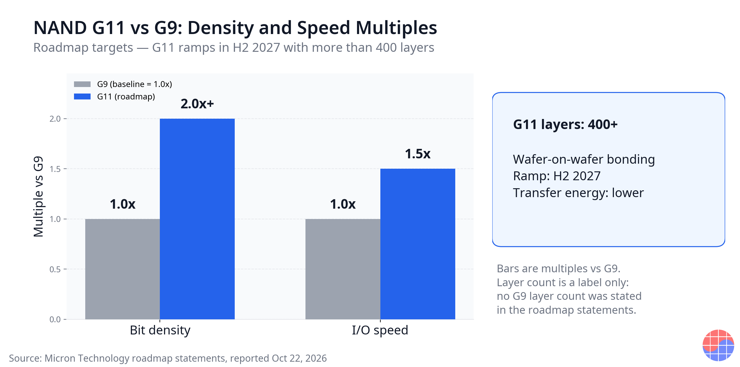
- NAND G11 is set to ramp in the second half of 2027 with more than 400 layers, wafer-on-wafer bonding, more than twice the bit density of G9, 1.5 times the I/O speed and lower transfer energy. AI-class NAND splits into high-IOPS SLC small-block designs and high-bandwidth NAND that stacks NAND with TSVs and places logic dies near compute.
Background
For decades, memory scaling rested on a simple premise: make the planar structure smaller. Pack cells more tightly, print them more precisely, and the same wafer yields more bits. The 4F-square cell that Micron tested for about 20 years belonged to that planar tradition. It was an attempt to push cell area close to a theoretical floor, yet after years of testing it never became the production path.
In roadmap statements reported on October 22, 2026, Micron changed that premise. Instead of extracting more from a flat layout, the company is redirecting capital toward stacking structures upward, bonding wafers together and rearranging logic in three dimensions. The shift is not limited to DRAM. The same roadmap covers a vertical turn for HBM, larger server RDIMMs, NAND beyond 400 layers and NAND designs built specifically for AI systems. It is less a single process decision than a structural reset across the whole memory portfolio.
One condition matters throughout. Everything in this article is a roadmap statement. Some items, such as 1-delta, are already in yield production. Others are much earlier: zeta angstrom is in early development, eta angstrom comes after it, and the G11 ramp is planned for the second half of 2027. A roadmap carries real information about direction and sequence, as stated by the company itself. It does not guarantee production, shipments or revenue, and it should be read with that gap intact.
Business Deep Dive
The DRAM node roadmap: from planar to 3D
| Node | Stage (per roadmap statements) | Key change |
|---|---|---|
| 1-delta | In yield production | Seventh-generation 10nm-class, density up 25% |
| 1-epsilon | Successor node | Introduces wafer bonding |
| zeta angstrom | Early development | First sub-10nm node, uses High-NA EUV |
| eta angstrom | After zeta | Applies experimental materials |
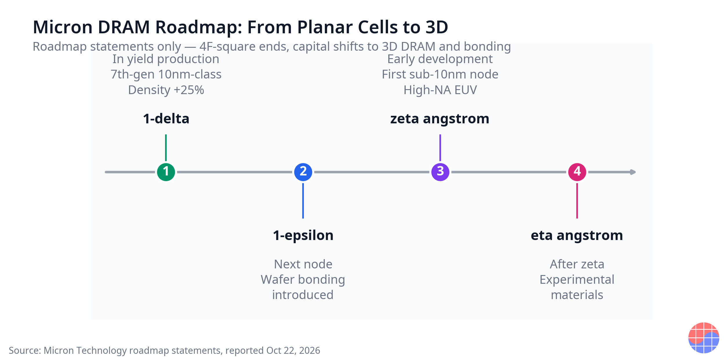
The roadmap starts from production, not from a concept. 1-delta, the seventh-generation 10nm-class node, is in yield production and delivers 25% higher density. That anchor matters: the sequence Micron described begins with a node that is already producing, rather than with a distant research target.
The next step, 1-epsilon, introduces wafer bonding. Bonding two wafers together has been a mainstream technique in image sensors, in NAND and in advanced packaging. Putting it explicitly into the main DRAM roadmap is the change. After that comes zeta angstrom, Micron's first sub-10nm node, now in early development and built around High-NA EUV. Eta angstrom follows zeta and applies experimental materials. The move into angstrom naming itself signals how the company frames the era after 10nm-class labels.
A structural change sits alongside the node names. DRAM CMOS logic is moving into 3D arrangements. The point is not only to stack cells. If the logic that drives the cells is also rearranged in three dimensions, designers can rethink routing length, area and power paths together. Place that next to the end of 4F-square and the picture is consistent: the center of gravity moves away from shrinking a planar cell and toward bonding and 3D logic.
HBM: vHBM and the CMOS condition for HBM4E
The key term for HBM is vHBM, a vertical HBM architecture. HBM already stacks DRAM dies vertically with TSVs. What Micron placed on the roadmap is a further step in that vertical direction. The statements did not provide a stacking method or figures for vHBM, so the supportable conclusion is about direction only: the next phase of HBM competition is becoming a contest of structure, not only of bandwidth numbers.
The CMOS comments split by generation. HBM4 did not need more advanced CMOS to meet Micron's power and performance targets, but HBM4E will. That single sentence matters because the company itself is acknowledging that the bottleneck is moving beyond the DRAM cell toward the logic CMOS, including the base die. It also explains why 3D DRAM and 3D arrangements of DRAM CMOS logic appear on the same roadmap. From the HBM4E generation onward, a memory maker's competitiveness will be judged on the sum of cell scaling, logic design and bonding skill, not on cell scaling alone.
Server and mobile memory: LPDDR6, DDR6 and a 1TB RDIMM
| Product | Roadmap statement | Reference point |
|---|---|---|
| LPDDR6 | 35% better power | Versus LPDDR5 |
| DDR6 | 2 times the bandwidth | Versus DDR5 |
| DDR5 RDIMM | 512GB module recently sampled | Current step |
| Next RDIMM | 1TB RDIMM planned | After the 512GB sample |
Product-level figures came with the roadmap. LPDDR6 is stated to deliver 35% better power than LPDDR5, and DDR6 targets twice the bandwidth of DDR5. On the server side, Micron recently sampled a 512GB DDR5 RDIMM and plans a 1TB RDIMM after it. As AI servers keep demanding more memory capacity and bandwidth per system, doubling RDIMM capacity changes the total memory pool a designer can fit at rack level. The same discipline applies here as everywhere else in this roadmap: these are targets and plans. Sampling is not mass production, and a plan is not a shipment.
📩 Following this story?
Get the follow-up analysis — earnings, reports and HBM supply — in your inbox daily at 10:30 KST. Subscribe free →
NAND G11: a ramp plan beyond 400 layers
| Item | G9 (baseline) | G11 (roadmap) |
|---|---|---|
| Layers | Baseline generation | More than 400 layers |
| Bit density | 1.0x (baseline) | More than 2.0x |
| I/O speed | 1.0x (baseline) | 1.5x |
| Transfer energy | Baseline | Lower |
| Bonding | — | Wafer-on-wafer bonding |
| Ramp timing | — | Second half of 2027 |
For NAND, G11 is the centerpiece. The ramp is planned for the second half of 2027, with more than 400 layers and wafer-on-wafer bonding. The performance targets are more than twice the bit density of G9, 1.5 times the I/O speed and lower energy per transfer. Layer-count competition in NAND has long been a contest of stacking height. The G11 statements differ in one respect: they explicitly tie a doubling of bit density to wafer-on-wafer bonding. If the cell wafer and the peripheral-circuit wafer are built separately and then bonded, each wafer can be optimized for its own process, instead of forcing both onto one compromised flow.
AI-class NAND: a fast tier and a bandwidth tier
What AI data centers ask of NAND is also changing. Micron presented AI-class NAND in two branches. The first is a high-IOPS SLC small-block design. It prioritizes input and output operations per second and responsiveness over raw capacity, which suits cache, metadata and other frequently accessed layers. The second is high-bandwidth NAND: NAND dies stacked with TSVs, with logic dies placed near compute. That design reframes NAND from cheap, bulk storage into another memory tier that sits next to the processor. Both branches are roadmap-stage design directions, not products. As signals, though, they are clear: in AI infrastructure, the boundary between storage and memory is blurring.
Chase's Take
The heaviest decision in this roadmap is not a launch. It is a cancellation. Ending a research path that ran for about 20 years is a technical judgment and, at the same time, a capital-allocation decision. Research organizations are structurally slow to kill their own long-running paths. The money already spent is large, the payoff picture is vivid, and both facts argue for one more year. Micron said, in public, that it would recognize that sunk cost and move finite capital into bonding and 3D structures instead. In management terms, the cancellation carries more information than any single new technology on the list, because it answers where the company intends to build its cost structure for the next decade.
The cost structure itself is moving. As bonding and 3D take the center, competition widens from the speed of lithographic shrinking toward bonding yield, stacking alignment and logic integration. The mix of equipment orders changes with it. The importance of leading lithography, including High-NA EUV, actually rises at the zeta step, while at the same time bonding, metrology and inspection tools move into the DRAM mainstream flow. For equipment makers, a memory maker's roadmap change is therefore also a change in what gets ordered.
The other management question is breadth. Micron is pushing DRAM, HBM and NAND at once, and at the level of structural change in each. Breadth lets the company address AI infrastructure as a whole, but it disperses capital and organizational focus. Narrow focus raises the odds of depth in one area and removes the buffer if the market moves elsewhere. This roadmap chooses breadth with structural change inside each area. Whether that choice works will not be decided by the announcement. It will be decided by bonding yield at 1-epsilon, by how Micron secures the advanced CMOS that HBM4E needs, and by whether the G11 ramp actually lands in the second half of 2027.
For Korean rivals, the point to watch is the change in the grammar of competition. As the contest widens from cell scaling to bonding and 3D integration, a larger share of the outcome sits outside the scaling lead that Korean memory makers have built. Read the other way, whoever locks in bonding yield and logic integration first takes the next generation's cost and performance together. Micron's cancellation should not be read only as one US company's decision. It is a signal that the criteria by which the whole memory industry is judged are moving.
Implications
- Watch the capital-allocation precedent. Ending a 20-year research path puts the same question to every memory maker: what costs more, keeping an aging path alive or closing it? Future roadmaps will reveal each company's answer.
- The equipment order mix changes. With wafer bonding entering the DRAM roadmap and wafer-on-wafer assumed for NAND G11, the memory share of bonding, metrology and inspection orders grows structurally. High-NA EUV demand is tied to the zeta step.
- HBM competition expands into logic competition. The statement that HBM4E will need more advanced CMOS means base-die and logic design capability becomes a larger variable with each HBM generation. Proposals such as vHBM sit in the same context.
- Separate roadmap from shipment. 1-delta is in yield production, zeta is in early development, and the G11 ramp is a plan for the second half of 2027. Investment and procurement decisions should read each item at its own stage, and no supply volume at any future date should be inferred from this roadmap alone.
- AI storage gains another tier. If high-IOPS SLC designs and near-compute high-bandwidth NAND are realized, the memory and storage hierarchy of an AI server divides more finely than the familiar three tiers of HBM, DRAM and NAND. System design and software optimization criteria change with it.
FAQ
Q1. What is the 4F-square architecture Micron is abandoning, and what replaces it? 4F-square is a planar DRAM cell architecture that Micron tested for about two decades. In roadmap statements reported on October 22, 2026, Micron said it is ending that path and shifting future capital to 3D DRAM. The replacement axes are wafer bonding, introduced at 1-epsilon, 3D arrangements of DRAM CMOS logic, and the vertical vHBM architecture.
Q2. How does the DRAM node roadmap run from 1-delta to eta angstrom? 1-delta is a seventh-generation 10nm-class node in yield production, with density up 25%. 1-epsilon introduces wafer bonding. Zeta angstrom is the first sub-10nm node, in early development, using High-NA EUV. Eta angstrom follows zeta and applies experimental materials. Later steps are earlier in development, and none of these statements is a confirmed shipment schedule.
Q3. What is vHBM, and how do the CMOS requirements of HBM4 and HBM4E differ? vHBM is a vertical HBM architecture, presented as a further step in HBM's vertical structure. On CMOS, Micron said HBM4 did not need more advanced CMOS to meet its power and performance targets, but HBM4E will. No generation performance figures beyond that statement are asserted here.
Q4. What are the plans for NAND G11 and AI-class NAND? G11 is planned to ramp in the second half of 2027 with more than 400 layers and wafer-on-wafer bonding, targeting more than twice the bit density of G9, 1.5 times the I/O speed and lower transfer energy. AI-class NAND was presented in two branches: high-IOPS SLC small-block designs, and high-bandwidth NAND with TSV-stacked NAND dies and logic dies placed near compute. All of these are roadmap statements, not shipped products.
Sources
- Micron Technology, roadmap statements reported October 22, 2026 — end of 4F-square and the shift to 3D DRAM; the 1-delta, 1-epsilon, zeta angstrom and eta angstrom nodes; vHBM; the HBM4E CMOS requirement; LPDDR6, DDR6 and RDIMM plans; NAND G11 and AI-class NAND directions
This article is for information only and does not recommend buying or selling any security. The roadmap items described are company statements as reported, not confirmed mass-production or shipment schedules.
📩 Missed today's analysis? Get tomorrow's in your inbox
Daily Silicon at 10:30 KST plus earnings and analyst-report breakdowns, first. Samsung Electronics, SK hynix, TSMC and HBM supply, read by practicing engineers. Join 300+ subscribers.
Subscribe free →
Free · No spam · Unsubscribe anytime