VLSI Korea
Wearable Semiconductors 1: The Smartwatch Brain War — Apple S10 vs Snapdragon W5+ Gen 2 vs Exynos W1000
No single winner in the smartwatch brain war. Exynos W1000 leads on specs with 3nm GAA and an A78 penta-core, W5+ Gen 2 leads on satellite and heterogeneous low-power design, and the S10 wins on vertical integration. Battery life is decided by power gating and STA, not the node number.


This is episode 1 of the Wearable Semiconductors series. The starting point, the episode 0 primer, is available at Semiconductors Inside Meta Glasses and the Oura Ring: What AR1, PSoC 6 and MAX86178F Actually Do.
30-Second Summary
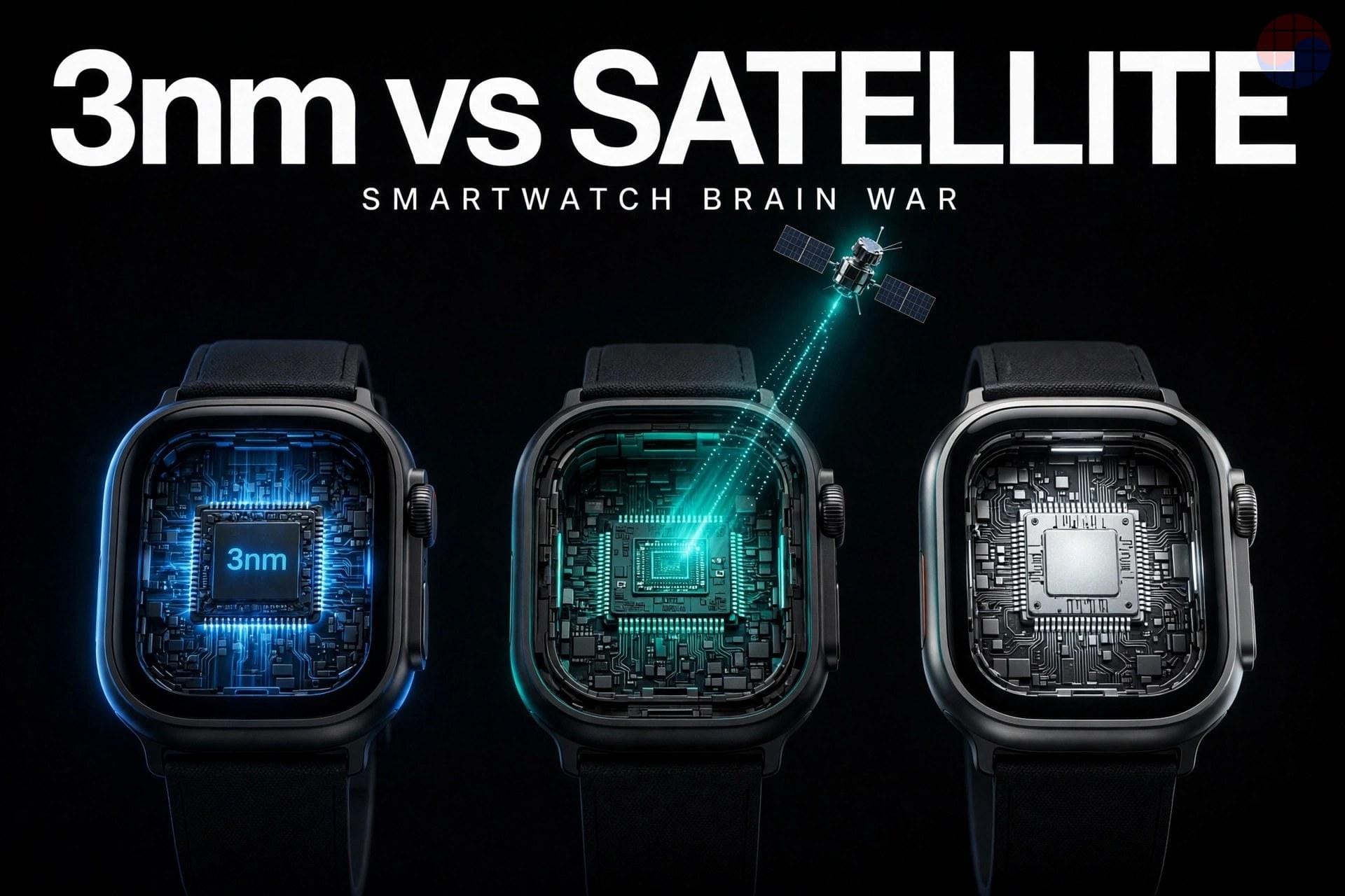
The verdict first: there is no single winner in the smartwatch brain war. Samsung's Exynos W1000 (announced July 3, 2024) leads on raw specifications, with a 3nm GAA process and a Cortex-A78 based penta-core CPU. Qualcomm's Snapdragon W5+ Gen 2 (announced August 20, 2025) leads on connectivity and heterogeneous low-power design, with NB-NTN satellite messaging via Skylo, a 22nm always-on co-processor and low-power islands. Apple's S10 (announced September 2024) wins on neither spec sheet; it wins on vertical integration and ecosystem efficiency. In wearables, battery life is decided less by the process node number than by power gating, STA (Static Timing Analysis) quality, and software scheduling.
Background: Why the Smartwatch SoC Matters Now
The smartwatch is the most brutally constrained power environment in consumer silicon. The battery on your wrist holds only a few hundred mAh, yet the device is expected to track heart rate, sleep and workouts all day and still last for days. At the same time, users now demand on-device AI. On-device Siri on Watch Series 10 and later, the Double Tap gesture, and sleep apnea notifications all require the device to process sensor streams continuously without waking the main CPU.
That means the contest between smartwatch SoCs is not about peak performance. It is about average power. The chip that wins is the one that covers the 23 hours when the screen is off, reading sensors, maintaining Bluetooth, and running background machine learning models without eating the battery alive. The three chips launched in 2024-2025, Apple S10, Snapdragon W5+ Gen 2 and Exynos W1000, attack this problem from three opposite directions, and the differences map directly onto each company's business model.
The Spec War: Three Chips by the Numbers
| Item | Apple S10 | Snapdragon W5+ Gen 2 | Exynos W1000 |
|---|---|---|---|
| Announced | Sep 2024 (Watch Series 10) | Aug 20, 2025 | Jul 3, 2024 (Galaxy Watch7/Ultra) |
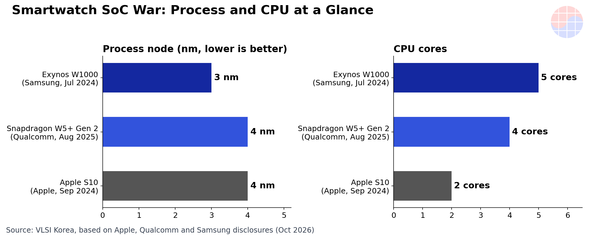
| Process node | TSMC 4nm-class (same generation as S9) | Main SoC 4nm (SWS5100), co-processor 22nm (QCC5100) | Samsung Foundry 3nm GAA (SF3, 2nd gen) - first 3nm wearable chip |
| CPU | Dual-core (based on A16 Bionic efficiency "Sawtooth" cores) | Quad Cortex-A53 up to 1.7GHz + co-processor Cortex-M55 at 250MHz | 1x Cortex-A78 1.6GHz + 4x Cortex-A55 1.5GHz (penta-core big.LITTLE) |
| GPU | Apple GPU (specs undisclosed) | Adreno A702 up to 1GHz | Mali-G68 MP2 |
| NPU / AI | 4-core Neural Engine | Hexagon V66K DSP + Ethos-U55 NPU (on co-processor) | NPU specs undisclosed (ML workloads supported) |
| Memory | 64GB storage | LPDDR4 2133MHz 16-bit | LPDDR5 |
| Connectivity | Bluetooth / Wi-Fi / LTE | NB-NTN satellite two-way emergency messaging (Skylo), Location ML 3.0, RFFE about 30% smaller | LTE Cat.4, 2.5D always-on display engine |
| Packaging | Thinner SiP, enabling the slimmer Series 10 case | SiP + always-on co-processor | FO-PLP, ePoP (DRAM+NAND), SiP with integrated PMIC |
| Launch product | Watch Series 10 (also Series 11, SE 3, Ultra 3 in 2025) | Google Pixel Watch 4 | Galaxy Watch7 / Watch Ultra |
Apple S10: Winning Without Changing the Process
The S10 debuted in September 2024 with Watch Series 10, and was carried into three 2025 product lines: Watch Series 11, Watch SE 3 and Watch Ultra 3. Look at the spec sheet and it is strikingly conservative. The TSMC 4nm-class process is the same generation as the S9 before it. The CPU is a dual-core design based on the A16 Bionic efficiency "Sawtooth" cores, paired with a 4-core Neural Engine and 64GB of storage. On numbers alone, it looks close to an S9 refresh.
Apple's real move was not in the process node but in SiP (System in Package) thickness. By thinning the S10's SiP, Apple built the slimmest Watch Series 10 case ever, and the internal volume recovered went straight into a larger display and battery. On-device Siri, the Double Tap gesture and sleep apnea notifications were implemented by binding the Neural Engine and the always-on sensor path together in software. Apple competed on integration, not on lithography. Reusing one chip across three product lines is the other half of the strategy: the classic Apple silicon platform play, amortizing one design across the entire watch portfolio.
Snapdragon W5+ Gen 2: Heterogeneous Computing Plus a Satellite
Qualcomm's W5+ Gen 2, announced August 20, 2025, makes the most aggressive architectural bet in this comparison. The main SoC (SWS5100) is a 4nm part with a quad Cortex-A53 cluster running up to 1.7GHz, an Adreno A702 GPU at up to 1GHz, LPDDR4 memory at 2133MHz on a 16-bit bus, and a Hexagon V66K DSP. The "+" in W5+ refers to the always-on co-processor (QCC5100) built on a 22nm process: a Cortex-M55 running at 250MHz with an Ethos-U55 NPU, plus low-power islands that independently run Wi-Fi, GNSS and audio.
Now do the power math. A single Cortex-A53 bursting at 1.7GHz consumes on the order of hundreds of milliwatts. A Cortex-M55 polling sensor data at 250MHz consumes on the order of single-digit milliwatts. If the screen is on for one to two hours of a 24-hour day, and the M55 island handles the other 22 hours while the A53 cluster sits in deep sleep, average power collapses. Cutting average power, not raising peak power, is the whole point of heterogeneous computing, and it is the design philosophy Qualcomm has pushed consistently across the W5 line.
Two platform-level differentiators ride on top. First, this is the first wearable platform with NB-NTN satellite two-way emergency messaging, delivered with Skylo: an SOS from a mountain trail or open water with no phone in reach, and the headline marketing hook of the Google Pixel Watch 4, its debut product. Second, Location ML 3.0 improves GPS accuracy by up to 50 percent in urban canyons, and the RFFE (RF front-end) shrank by roughly 30 percent. Area saved on the RF front-end is mechanical freedom handed back to the OEM.
Exynos W1000: Samsung's 3nm GAA Showcase
Samsung's Exynos W1000, announced July 3, 2024, is the only chip of the three built on a 3nm process, and not just any 3nm: Samsung Foundry's second-generation 3nm (SF3) GAA (Gate-All-Around). The title of "first 3nm wearable chip" is itself the message. The CPU is a penta-core big.LITTLE configuration: one Cortex-A78 big core at 1.6GHz plus four Cortex-A55 little cores at 1.5GHz. The GPU is a Mali-G68 MP2 and memory is LPDDR5.
Samsung's claimed numbers versus the previous W930 are 3.4x single-core performance, 3.7x multi-core performance and 2.7x faster app launches. Let us sanity-check the arithmetic. The Cortex-A78 has roughly 20-30 percent higher IPC (instructions per clock) than the Cortex-A55. Add the 1.6GHz versus 1.5GHz clock difference and one big core delivers about 1.3-1.4x the single-thread performance of a little core. So where does 3.4x come from? Two places. First, the W930 baseline was a dated dual-core-class architecture, and a low baseline inflates any multiplier. Second, the power efficiency of 3nm GAA lets the chip hold higher clocks longer within the same power budget, which is an improvement in sustained performance, not just burst numbers. The 3.7x multi-core figure reads as the penta-core count increase combined with GAA's leakage current reduction.
The packaging story deserves attention too. FO-PLP (fan-out panel-level packaging), ePoP (embedded package-on-package) stacking DRAM and NAND, and a SiP with an integrated PMIC: the W1000 is the full Samsung in-house stack in one part. With LTE Cat.4 and a 2.5D always-on display engine, it powers the Galaxy Watch7 and Watch Ultra. And remember what GAA really buys a wearable: not peak clocks, but lower leakage in the always-on state. A smartwatch spends 23 hours of its day in that state.
Chase's Take: The Node Number Is Half the Story
I work in STA and signoff timing, so I am skeptical of anyone who grades a chip by its process node number alone. What matters is not whether it is 3nm or 4nm, but how the design was closed. On the same 4nm process, clock tree synthesis quality, power gating granularity and multi-corner STA rigor can swing real battery life by tens of percent. The reason Apple kept Series 10 battery life without changing the process is, in my view, SiP integration and software scheduling doing the heavy lifting, not the silicon itself.
The strategic intents are equally legible. For Samsung, the W1000 is not just a watch chip; it is a 3nm GAA showcase. Samsung Foundry needed proof, in front of external customers, that SF3 yields and runs in a power-sensitive product, and its own watch became that proof. For Qualcomm, the W5+ Gen 2 is a platform sale: it sells OEMs like Google a story ("ship our chip and you can market satellite SOS and 50 percent better GPS"), with the heterogeneous architecture as the technical evidence. For Apple, the S10 is whole-widget optimization: not the chip spec in isolation, but the watch's thickness, battery and sensor experience taken together, with one chip across three lines delivering economies of scale.
One more note. All three vendors spotlight their NPU blocks, but the wearable AI contest is not about TOPS numbers. Workloads like Double Tap recognition or sleep apnea detection are always-on inference in the hundreds of GOPS, and the real question is whether first-pass filtering happens at the sensor hub level without waking the NPU at all. Qualcomm's M55 plus Ethos-U55 island targets exactly that tier. Apple reaches the same effect by binding the Neural Engine and sensor path at the OS level. In the end, how many tiers your power hierarchy has is the central design question for a wearable SoC.
Implications: Who Gets What
For vendors: Samsung Foundry gains a reference design for SF3 GAA, and one more line in its customer pitch: "shipping in our own product." TSMC keeps the Apple S10's 4nm-class volume and its position as the most proven wearable partner. Qualcomm gets a beachhead to extend its Skylo satellite partnership beyond wearables into other form factors.
For OEMs: Google gets the satellite SOS story exclusively for the Pixel Watch 4. Samsung Electronics runs its own performance marketing (3.4x, 3.7x) on its own silicon. Apple simplifies its cost structure by covering three lines with a single chip.
For users: The good news is that all three chips aim at AI that saves battery rather than AI that drains it. More on-device processing means fewer cloud round trips, which translates into privacy and responsiveness. One caveat: features like satellite SOS require coverage and plan checks. Chip support does not mean the service works everywhere.
FAQ
Which of the three chips is the fastest?
On spec-sheet numbers, the Exynos W1000. The evidence is its 3nm GAA process, Cortex-A78 based penta-core CPU, and Samsung's claimed 3.4x single-core and 3.7x multi-core gains over the previous generation (announced July 3, 2024). Real-world responsiveness, however, depends heavily on software optimization.
How does satellite messaging on the Snapdragon W5+ Gen 2 work?
It connects to Skylo's satellite network using the NB-NTN (Narrowband Non-Terrestrial Network) standard, enabling two-way emergency messaging where there is no cellular coverage. It is the first wearable platform to support this (announced August 20, 2025) and debuted in the Google Pixel Watch 4. Separate plan or regional availability conditions may apply.
Why is the Apple S10 competitive without a process change?
The S10 uses the same TSMC 4nm-class generation as the S9, but its thinner SiP enabled the slimmest Watch Series 10 case, and the recovered volume went to the display and battery. Features like on-device Siri and Double Tap are implemented through the 4-core Neural Engine and software integration. Apple's strategy is whole-product optimization, not a chip spec race.
What is the most important metric for a wearable chip?
Average power, not peak performance. Battery life is decided by how the chip survives the 20-plus hours with the screen off, which comes down to its power hierarchy. Qualcomm answers with a 22nm always-on co-processor and low-power islands, Samsung with 3nm GAA leakage reduction, and Apple with SiP integration and OS-level scheduling.
* Figures in this article are based on materials disclosed by Apple, Qualcomm and Samsung in 2024-2025 (as of October 22, 2026). Actual product performance and battery life vary with usage conditions.
Back to the series hub: Wearable Semiconductors Primer - Semiconductors Inside Meta Glasses and the Oura Ring
📩 Subscribe to VLSI Korea
Get our daily semiconductor deep-dives delivered to your inbox first. Free to subscribe.