VLSI Korea
Inside Meta glasses and Oura Ring: what AR1, PSoC 6 and MAX86178F actually do
Explore AR1, PSoC 6 and MAX86178F with product images and worked examples of image bandwidth, optical sensing, power and memory.


The processor behind a photograph on Ray-Ban Meta glasses is Qualcomm's Snapdragon AR1 Gen 1. In Oura Ring 4, an Infineon PSoC 6-family MCU and Analog Devices MAX86178F analog front end handle embedded control and physiological-signal acquisition. The glasses process bursts of camera and audio data; the ring repeats optical measurements on a small battery.
That difference changes the silicon priorities. Glasses need image throughput and memory bandwidth. A ring needs optical signal quality and a low average power budget. The examples here are the 2023 Ray-Ban Meta and Oura Ring 4, connecting their chips to data flow, power and physical integration.
Wearable performance comes from more than the main processor. Acquisition circuits, memory transfers and power control work together to determine how long the product can operate.
1. Start with the chip map
Meta and Qualcomm identify AR1 in their product announcements. TechInsights identifies the PSoC 6 family, MAX86178F and Bosch accelerometer in its teardown of the Oura Ring 4 sample JZ90-54218-15. Meta · Qualcomm · TechInsights
| Product | Semiconductor | Job in the system | Source |
|---|---|---|---|
| Ray-Ban Meta, 2023 | Qualcomm Snapdragon AR1 Gen 1 | Image, audio and application processing | Meta / Qualcomm announcement |
| Oura Ring 4 | Infineon PSoC 6 family | Sensor control and embedded processing | TechInsights teardown |
| Oura Ring 4 | Analog Devices MAX86178F | Analog acquisition of physiological signals | TechInsights teardown |
| Oura Ring 4 | Bosch Sensortec accelerometer | Motion sensing | TechInsights teardown; model not disclosed |
| Oura Ring 4 | LEDs and photodiodes | Emit light and detect reflected light | Oura / TechInsights |
| Design example | Texas Instruments BQ25120A | Charging, voltage conversion and load control | TI datasheet; reference component |
AR1 is a system-on-chip integrating several processing functions. PSoC 6 is a microcontroller that runs embedded code and controls peripherals. MAX86178F sits nearer the sensor, acquiring small electrical signals. The useful organizing principle is sensor → AFE → MCU/SoC → memory → wireless, with each component assigned to its place in that path.
The ring's LEDs and photodiodes are semiconductors too. LEDs turn current into light; photodiodes turn received light into current. Tissue sits between them, the AFE reads the resulting current, and the MCU coordinates illumination and acquisition.
2. Snapdragon AR1: the processing behind one camera
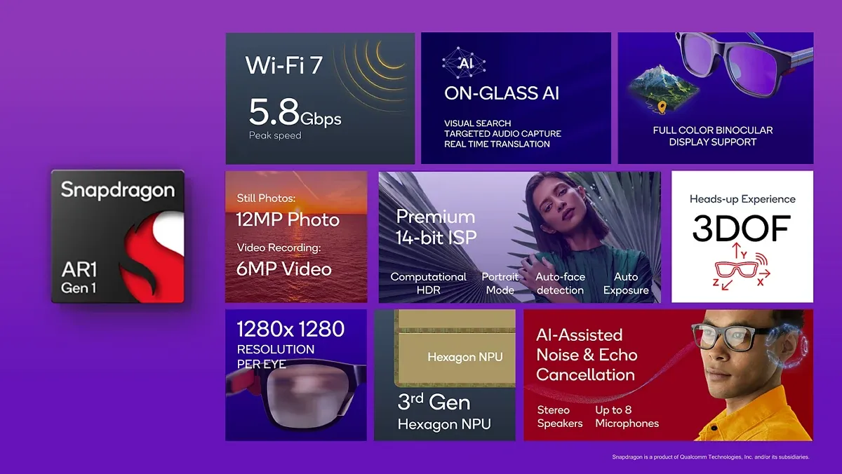
The 2023 Ray-Ban Meta has a 12 MP camera and five microphones. Qualcomm describes AR1 through dual ISPs, its third-generation Hexagon NPU, image and audio processing, and power optimization. Specialized blocks divide the workload instead of assigning every pixel operation to a CPU. Meta announcement · AR1 product information
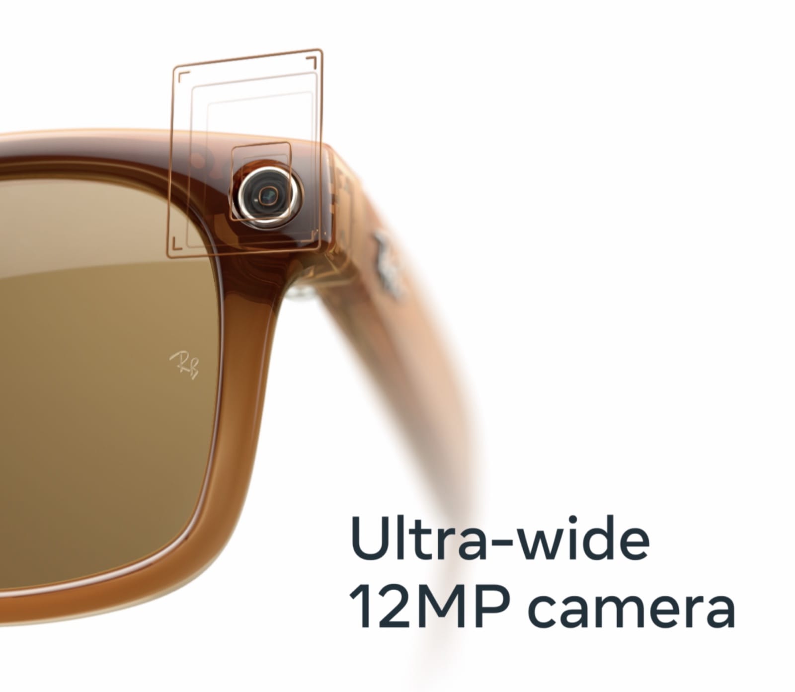
An image sensor outputs pixel samples. An image signal processor, or ISP, performs operations such as color reconstruction, noise reduction, exposure processing and color adjustment. With a Bayer-filter sensor, for example, each photosite samples only part of the color information; neighboring samples help reconstruct the color image.
An encoder then produces a representation suitable for storage or transmission. A neural processor executes model operations, while the CPU runs software and coordinates control. The same frame can become an improved image in the ISP, a bitstream in the encoder and a model output in the NPU. Dedicated processing reduces the need for the CPU to repeatedly copy and calculate over large pixel arrays.
| AR1 platform block | Main workload | Engineering pressure |
|---|---|---|
| ISP | Image formation and enhancement | Pixel throughput, line buffers, noise |
| Hexagon NPU | Neural-network processing | Model size, precision, memory traffic |
| CPU | Control and software execution | Response time, interrupts, scheduling |
| Audio processing | Voice capture and enhancement | Microphone synchronization, latency |
| Memory / connectivity | Buffering and data transport | Bandwidth, transfer energy, retries |
Platform functions from Qualcomm documentation; the product configuration in this article is the 2023 Ray-Ban Meta.
A design example makes the bandwidth problem concrete. A 12 MP frame at 12 bits per pixel occupies 18 MB. A hypothetical 30-frame-per-second input requires 12,000,000 × 12 ÷ 8 × 30 = 540 MB/s before compression.
One processing stage that writes and then rereads that intermediate image moves 540 × 2 = 1,080 MB/s. These transfers are additional work beyond receiving the sensor input. Line buffers, direct block-to-block transfer and fewer memory accesses therefore matter as much as the arithmetic performed on a frame.
The size of the saved photo hides this intermediate traffic: the file is already compressed. During processing, larger frames and working buffers may exist. Keeping a complete frame in memory and processing it a few lines at a time also lead to different storage and latency requirements.
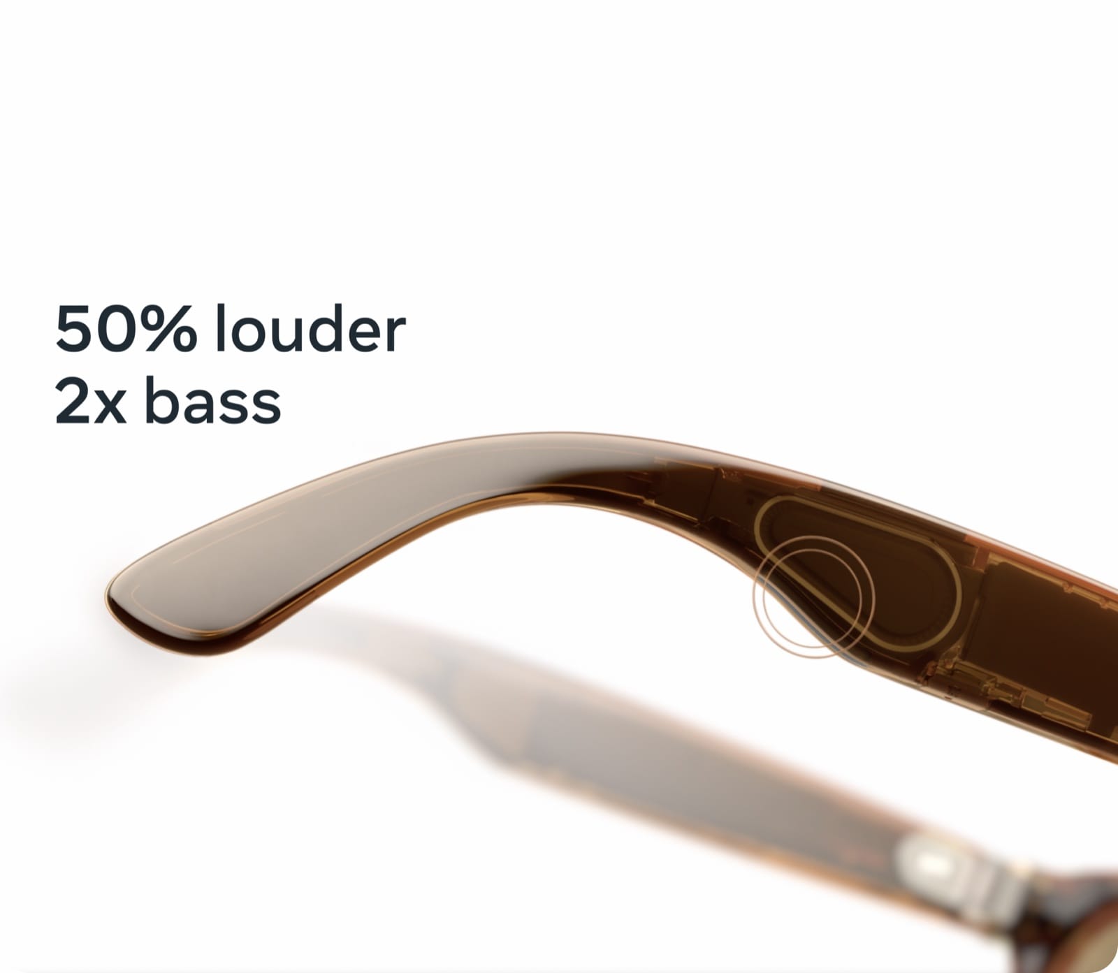
Five microphones contribute spatial information
Microphones at different positions receive sound at different times and levels. Processing those differences can emphasize speech from a desired direction or reduce competing noise. Echo cancellation addresses another path: sound emitted by the speakers that re-enters the microphones.
For an illustrative audio path, five channels sampled at 48 kHz with 24-bit PCM produce 5 × 48,000 × 24 = 5.76 Mbit/s, or 720 kB/s. This is smaller than the image stream, but synchronized sampling, continuous processing and short latency are central requirements.
A 10 ms processing block contains 480 samples per channel at that rate. Larger blocks reduce invocation frequency but increase how long the earliest sample waits. Users notice that delay in calls and voice interaction, making buffer length and execution priority important alongside throughput.
3. Oura Ring 4: turning reflected light into data
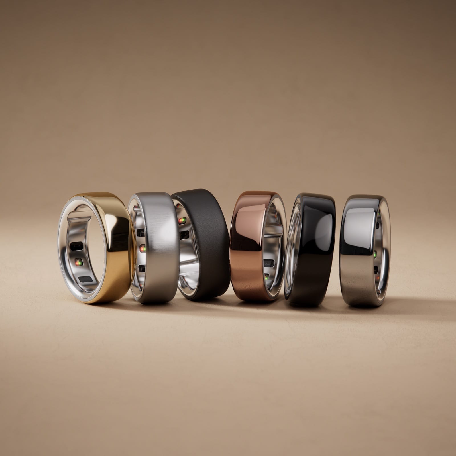
Oura Ring 4 uses multi-wavelength PPG, digital temperature sensing and an accelerometer. Its Smart Sensing system selects suitable measurement paths from 18 optical signal paths. The TechInsights teardown describes two multi-color LEDs and three photodiodes. Oura technology · Smart Sensing · Teardown
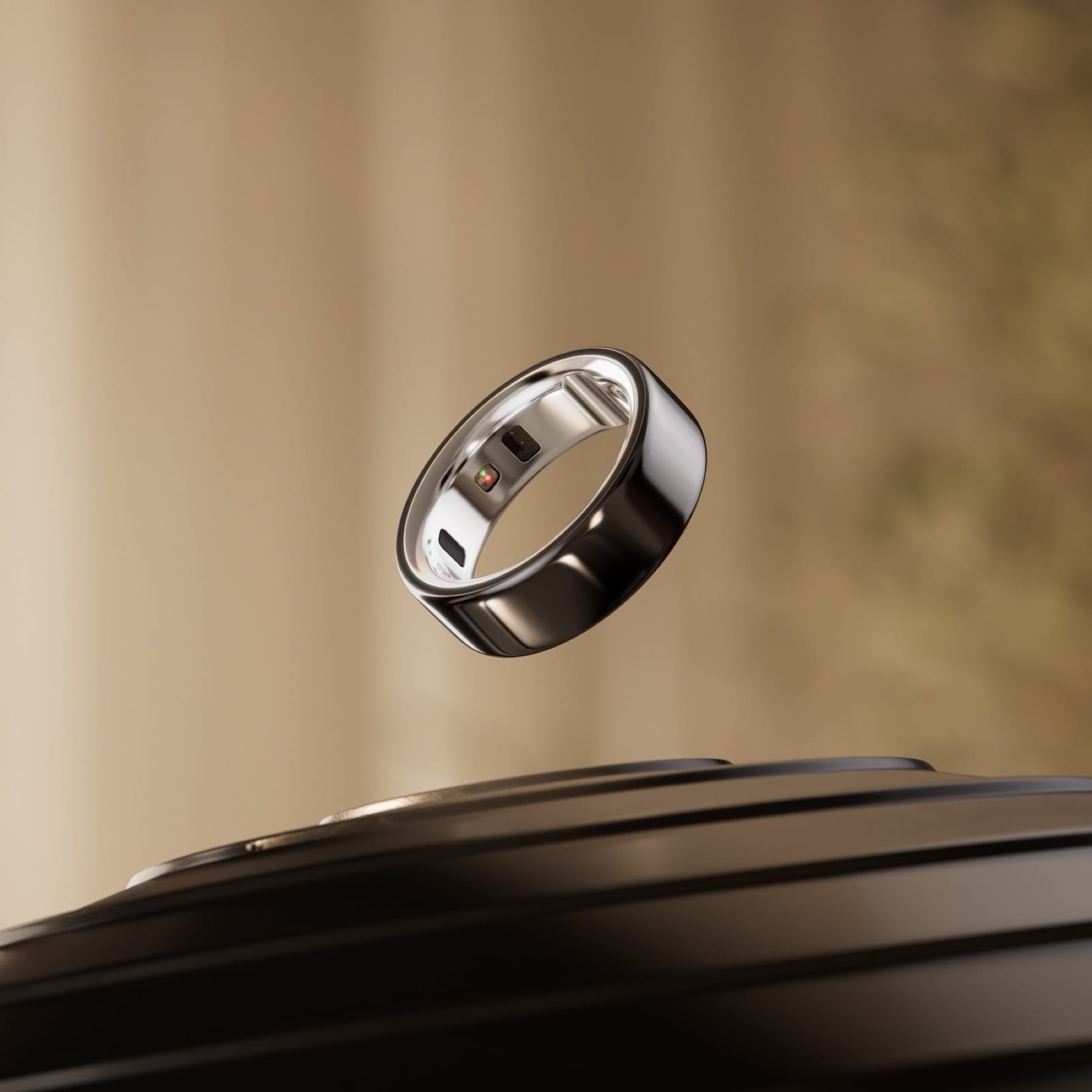
Photoplethysmography, or PPG, measures changes in received optical signals over time. Light enters tissue, where some is absorbed and some returns to a detector. The photodiode converts that light into current. Small pulsatile changes ride on a larger background component.
The analog front end converts the detector current into an electrical representation it can acquire, handles offsets and ambient light, and digitizes the result. Simply increasing gain can push the input out of range when the background signal is large. LED current, integration time, receiver range and sampling must be designed together.
ADI's public MAX86178-family documentation describes support for up to six LEDs and four photodiode inputs, two optical readout channels with independent 20-bit ADCs, and ambient-light cancellation. It illustrates how source selection and low-level optical acquisition can be integrated into one AFE. ADI MAX86178
A 20-bit converter has 2²⁰ = 1,048,576 codes. The analog design problem is to resolve a pulsatile signal amid noise while using the converter's input range effectively and avoiding saturation. This is why ADC resolution and system signal-to-noise ratio belong in the same design discussion.
| Ring signal path | Semiconductor task | Useful design variable |
|---|---|---|
| LED → tissue | Optical excitation | Wavelength, pulse current, pulse width |
| Tissue → photodiode | Light-to-current conversion | Optical coupling, detector area |
| Photodiode → AFE | Acquisition and digitization | Ambient rejection, integration, ADC range |
| AFE → MCU | Timing, buffering and processing | Interrupt rate, transfer size, filtering |
| MCU → memory / phone | Retention and synchronization | Data reduction, latency, radio activity |
PSoC 6 operates the measurement process: configure the sensors, respond when measurements finish, retrieve data, and pass it to filtering, storage and communication tasks. Designing good analog acquisition and ensuring the processor retrieves data on time are separate engineering jobs.
The dual-core PSoC 6 family combines Cortex-M4 and Cortex-M0+ processors. Infineon's system-design documentation specifies maxima of 150 MHz and 100 MHz respectively and describes shared memory and interprocessor communication. This family architecture supports separating more demanding computation from lighter control tasks. Infineon AN215656
Partitioning work also creates coordination costs. Locking and unlocking a shared buffer on every sensor event can be expensive. Collecting a batch before handing over ownership reduces exchanges, at the cost of memory and latency. Low-power control involves reducing wakeups and data transfers as well as choosing a clock frequency.
The accelerometer adds a motion signal. Comparing optical disturbance with time-aligned acceleration can help interpret motion contamination. Temperature contributes information on another timescale. Combining these streams makes timestamps and alignment part of the sensor-system design.

4. Multi-day operation is an average-power problem
Consider a design example with a 3.8 V, 20 mAh battery and a seven-day target. Nominal energy is 3.8 × 20 = 76 mWh; duration is 7 × 24 = 168 h. The average power budget is 0.452 mW, or 0.362 mW if usable energy is assumed to be 80% of nominal.
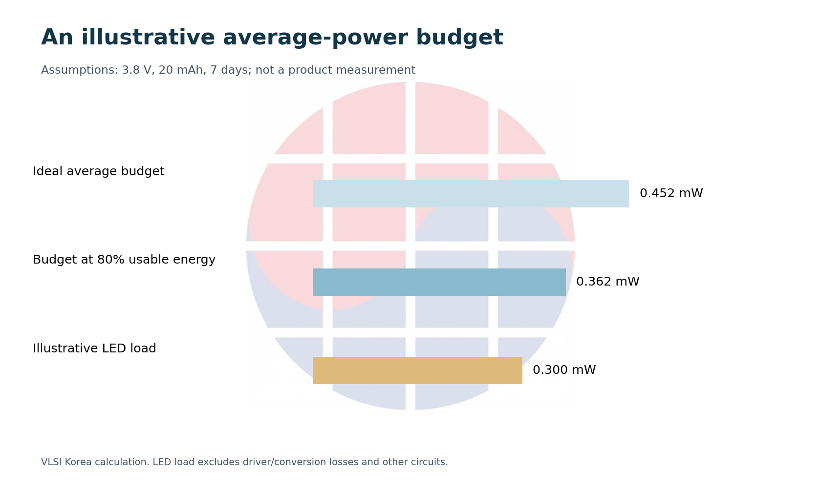
Now add an LED driven at 10 mA for 100 µs, 100 times per second. Its duty cycle is 1%, and average current is 0.1 mA. At an assumed 3.0 V LED voltage, the optical-source load is 0.3 mW. Even before driver losses, it consumes most of the example's 0.362 mW load budget.
Changing pulse duration, frequency or current can therefore matter more than a modest improvement in processor speed. Reducing illumination also changes the acquired signal. The optimization target is the minimum optical energy that achieves the required signal quality.
Average power can be expressed as Pavg = Σ(Pi × ti) ÷ T. Separating optical acquisition, processing, synchronization and sleep states exposes which activities consume the budget and which frequencies can usefully change.
Short transfers still matter when repeated. In another design example, a 10 mW load active for one second every minute averages 10 ÷ 60 = 0.167 mW. One second every five minutes averages 10 ÷ 300 = 0.033 mW. Batching and application-update latency become battery-life decisions.
Optical pulse width, processor wakeup frequency and wireless batch size all draw from the same average-power budget.
The PMIC distributes power as well as charging the battery
Sensors and processors need different voltages and noise conditions. A power-management IC converts battery voltage, disconnects unused loads and controls charging. Its own consumption also matters during long idle periods.
TI's BQ25120A, a wearable power-circuit reference, integrates a charger, buck converter and LDO/load switch. TI specifies 700 nA typical quiescent current with the buck enabled at no load. This is a useful example of the regulator overhead that matters at light load. TI BQ25120A
An LDO's load-related dissipation is Ploss = (Vin − Vout) × Iload. Supplying a 1.8 V, 1 mA load from 3.8 V consumes 1.8 mW at the load and dissipates 2.0 mW in the LDO. Ideal efficiency, excluding quiescent current, is about 47%.
A buck converter can reduce this conversion loss, but introduces an inductor, switching noise and light-load operating choices. A sensitive analog rail may use an LDO after a buck. The decision combines energy efficiency, board area and acquisition noise.

5. Memory and BLE: how much signal should survive?
An illustrative stream of three-byte samples from four channels at 100 samples per second produces 1,200 bytes/s. Over a day, that is 1,200 × 86,400 = 103,680,000 bytes, or 103.68 MB, before headers and timestamps.
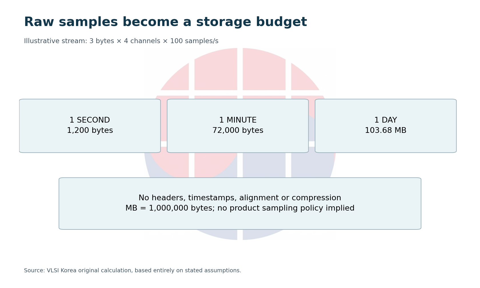
Ten minutes requires 720 kB. A 32 KiB buffer holds approximately 32,768 ÷ 1,200 = 27.3 seconds. Buffer capacity therefore defines how long the processor can wait before draining the stream. Competing tasks must leave enough time to meet that deadline.
A FIFO can accumulate samples and trigger an interrupt at a threshold instead of waking the processor for each sample. Where supported, DMA moves data between peripherals and memory without CPU-driven copies. Reduced processor activity creates more sleep time and scheduling headroom.
| Data strategy | Storage / radio effect | Design cost |
|---|---|---|
| Keep raw samples | Highest retained detail | Larger buffers and transfer volume |
| Compress samples | Smaller representation | Codec compute and metadata |
| Keep selected features | Compact summaries | Less detail for later reprocessing |
| Batch transfers | Fewer transfer sessions | More buffering and delivery delay |
Wireless activity includes connection events, headers and retries in addition to useful payload. Frequent small packets can extend active time despite a low data rate. Larger batches need more memory and deliver updates later.
Where reduction happens matters too. Moving all raw samples out of an AFE before reducing them leaves that first bus transfer unchanged. Selecting necessary data earlier can reduce subsequent memory and radio work. A decision near the start of the data path propagates through several downstream power consumers.
6. The remaining engineering happens around the chips

Glasses temples must accommodate compute, power, batteries and audio hardware. A ring must place its sensors toward the skin and align optical windows in an even tighter space. Board, optics and mechanical engineering connect small silicon to a wearable product.
A small WLCSP can reduce package footprint, while fine contact pitch increases routing and assembly demands. A system-in-package can move board-level connections inside a package. Internal interconnect, heat, test coverage and yield then become package-level design concerns.
In the optical section, direct leakage from an LED into a photodiode creates a path that bypasses tissue. Window placement, optical barriers, spacing and alignment affect the background signal. A different optical assembly can require different LED current and receiver settings even with the same AFE.
Metal enclosures and the body change the antenna environment. Leaving placement and matching until after board completion increases redesign risk. Evaluating connectivity in the worn configuration alongside circuit and mechanical design also helps control energy spent on retransmissions.
Thermal design includes sustained and transient loads. Long recording or upload activity can concentrate processing and radio power in a small area of a glasses temple. The path into the enclosure, skin-contact geometry and workload duration influence temperature rise. Sustainable throughput can become thermally limited before total battery energy is exhausted.
The two products thus prioritize different circuits. AR1-centered glasses must process frames and audio on time while controlling data movement and heat. An Oura-style sensing system must acquire useful low-level signals while carefully budgeting activity across the light sources, AFE, MCU and radio. That distinction is the starting point for selecting wearable silicon.
Sources
- Meta, Ray-Ban Meta announcement, September 27, 2023.
- Qualcomm, AR1 and XR2 announcement, September 27, 2023.
- Qualcomm, Snapdragon AR1 Gen 1, platform functions.
- Oura, Ring 4 technology, March 18, 2025.
- Oura, Smart Sensing, October 3, 2024.
- TechInsights, Oura Ring Gen 4 Teardown, May 22, 2025.
- Analog Devices, MAX86178, family documentation.
- Infineon, AN215656, dual-core system design.
- Texas Instruments, BQ25120A, power-circuit reference.
Sources checked and article revised September 29, 2026. Prepared with AI assistance. Design-example inputs are stated alongside each calculation.
Disclosure
This article is provided for informational purposes only and does not constitute a recommendation to buy or sell any security. Figures and factual statements are based on publicly available sources, including company filings, news reports, and market research, and may contain errors in the source material or in the preparation of this article. The author may own shares in companies mentioned. All investment decisions and their outcomes are the reader's responsibility.
📚 Series Contents
- Episode 0: Inside Meta Glasses and the Oura Ring (primer)
- Episode 1: The Smartwatch Brain War — Apple S10 vs Snapdragon W5+ Gen 2 vs Exynos W1000