HBM4: Micron vs SK hynix vs Samsung

Executive summary
- HBM4 changes the scaling axis: instead of pushing only pin rate, JEDEC doubles the bus width to 2048-bit and channels to 32 per stack, delivering ~2 TB/s per stack at 8 Gb/s—a structural shift from HBM3(E). (Tom's Hardware)
- Vendors are already exceeding the baseline: NVIDIA is pushing suppliers toward 10 Gb/s bins; Micron has sampled >11 Gb/s / >2.8 TB/s stacks. Expect SKU segmentation by speed/stack height. (Tom's Hardware)
- Packaging is the new moat:
- SK hynix leans on Advanced MR-MUF (warpage/thermals) and is furthest along on 12-Hi HBM4 sampling and ramp prep in 2H25. (SK hynix Newsroom -)
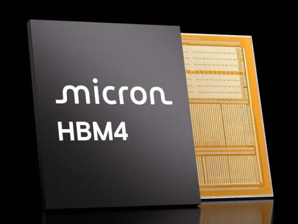
- Micron differentiates with in-house base die and high-speed bins; HBM4E adds customizable base-die (with TSMC) for premium SKUs. (Micron Technology)
- Samsung plans hybrid Cu bonding (HCB) for HBM4 and is reportedly using a 4 nm node for the logic/base die to chase high-speed stability. (Tom's Hardware)
What HBM4 actually changes (vs HBM3/E)
HBM4 formalizes 2048-bit I/O and 32 independent channels (each split into two pseudo-channels) so you can hit ~2 TB/s at 8 Gb/s without extreme SI/PDN pain. It’s a bandwidth-at-width strategy that plays better with thermal and signal-integrity budgets than brute-forcing frequency alone. (Tom's Hardware)
High-end accelerators, however, want more: NVIDIA is pressing suppliers for 10 Gb/s to stay ahead of AMD’s next-gen parts—so real platforms will mix standard 8 Gb/s stacks with 10–11 Gb/s bins at the top. That raises power/cooling and timing-margin risk, which is why packaging choices (bonding, underfill, interposer copper) now dominate the discussion. (Tom's Hardware)
Head-to-head: Micron vs SK hynix vs Samsung (HBM4)
| Category | Micron | SK hynix | Samsung |
|---|---|---|---|
| I/O Configuration | 16-channel × 128-bit (2048-bit total) | 16-channel × 128-bit (2048-bit total) | 16-channel × 128-bit (2048-bit total) |
| Bandwidth (Gbps per pin) | Up to ~11 Gbps (sample) | 10 Gbps+ (exceeds JEDEC 8 Gbps) | ~10 Gbps (targeting 11 Gbps for NVIDIA) |
| Total Bandwidth (per stack) | ~2.8 TB/s @11 Gbps | ~2.5 TB/s @10 Gbps | ~2.5 TB/s @10 Gbps |
| Capacity (GB per stack) | 36 GB (12-Hi, 24Gb) → up to 64 GB (16-Hi, 32Gb) | 36 GB (12-Hi) → up to 64 GB | 36–64 GB |
| Stack Height (Hi) | 4–16 Hi | 4–16 Hi | 4–16 Hi |
| Energy Efficiency (pJ/bit) | Not disclosed (claimed industry-leading) | ~2.4 pJ/bit | ~2.0 pJ/bit |
| Sampling Schedule | Mid-2025 | Early 2025 (world’s first HBM4 samples) | Late 2025 |
| Mass Production | 2026 (target) | Q4 2025 (initial ramp-up) | Late 2025 → full volume in 2026 |
| DRAM Fab Location | Hiroshima, Japan | Icheon, Korea | Pyeongtaek, Korea |
| Production Target | 20% of total DRAM output | Largest HBM capacity among peers | Rapid ramp-up for early mass production |
| DRAM Process Node | 1γ (1-gamma) nm-class (~10nm) | 1b nm (5th-gen 10nm) | 1c nm (3rd-gen 10nm) |
| Base Die Process | Advanced CMOS (in-house) | 12FFC+ / 5nm FinFET | 4nm FinFET |
| Base Die Foundry | Micron (in-house) | TSMC | Samsung Foundry |
| Stacking Method | Micro-bump TSV, TCB bonding | Micro-bump TSV (thermal compression) | Hybrid Cu bonding (HCB) |
| Underfill Material | Standard underfill | MR-MUF | NCF |
| Max Stack Height | 12-Hi (36 GB) → supports 16-Hi | 12-Hi → supports 16-Hi | Optimized for 16-Hi (+33% density via HCB) |
| Interposer | 2.5D silicon interposer | 2.5D silicon interposer | 2.5D silicon interposer |
Sources: JEDEC HBM4 overview; NVIDIA push to 10 Gb/s; Micron Q4-FY25 remarks; SK hynix press/Reuters; Samsung hybrid bonding and 4 nm reports. (HPCwire)
What this means for your system
1) Choose your bin strategy (not just capacity)
- If your thermal budget is tight or you’re interposer-area-constrained, 8–10 Gb/s bins can deliver better TCO than chasing 11 Gb/s headline numbers—especially for inference-dense configurations. NVIDIA’s 10 Gb/s ask is a warning: power and signal margins will be your gating factors. (Tom's Hardware)
2) Treat the base die as the lock-in surface
- With HBM4, meaningful differences move below DRAM: PHY topology, routing, on-die monitors, and PDN behavior in the base logic die. Micron’s in-house base die (HBM4) and customizable base die for HBM4E increase stickiness. If you want multi-sourcing, constrain vendor-specific base-die features up front. (Micron Technology)
3) Packaging is a first-order performance knob
- Hybrid Cu bonding (HCB) reduces inter-die resistance and improves thermals—attractive for 16-Hi and high-speed bins. Samsung is aligning HBM4 to HCB, while SK hynix relies on Advanced MR-MUF for warpage/thermal control and fast 12-Hi maturity. Match bonding to your target speed and service-life profile. (Tom's Hardware)
4) Timeline risk & capacity
- SK hynix has the clearest near-term ramp (samples in Mar 2025; internal cert done; 2H25 prep). Micron has the fastest samples today and is talking 2026 for broader volume. Samsung is arming for a 2026 surge with HCB + 4 nm. Build buffer for qualification loops and packaging-line slots. (SK hynix Newsroom -)
Due diligence checklist (use with all three vendors)
- Thermal map & PDN: ΘJA/ΘJC across 12-Hi and 16-Hi; hotspot gradients under your airflow plan; interposer copper density and IR-drop headroom.
- Stack-height yield: 12-Hi vs 16-Hi yield curves; rework policy; RMA root-causes (TSV voids, delam, EM).
- Base-die options: What’s customizable vs standard? Tooling/PDK constraints? What’s the escape plan if you multi-source? (Micron’s HBM4E customization is the bar.) (Micron Technology)
- Line capacity & lead time: Bonding choice (HCB vs micro-bump) affects takt time; lock packaging slots early.
Speed margin at target bin
: Eye openings, CTLE/DFE settings, per-channel skew, error behavior vs pattern/burst. (Ask for 10 Gb/s data even if you’ll ship 8–9.5 Gb/s.) (Tom's Hardware)
Bottom line
The HBM4 era is memory-centric system design. Pick your speed/stack bins based on platform thermals and lifetime reliability, design your interposer + PDN around realistic margins, and negotiate base-die features like you would a custom ASIC. If you need the earliest stable supply, SK hynix leads on timeline; if you want headline speed and future custom base-die leverage, Micron is setting that agenda; if you want HCB + 4 nm upside for high-speed 16-Hi, Samsung deserves a fresh look. (SK hynix Newsroom -)