HBM4 to HBM8 Roadmap: Architecting the Future of AI Compute

The High Bandwidth Memory (HBM) roadmap from HBM4 to HBM8 represents a transformative leap in memory architecture to meet the escalating demands of AI supercomputing, particularly for large language models (LLMs), generative AI, and eventual AGI/ASI systems.
HBM4 (2026, NVIDIA Rubin, AMD MI400)
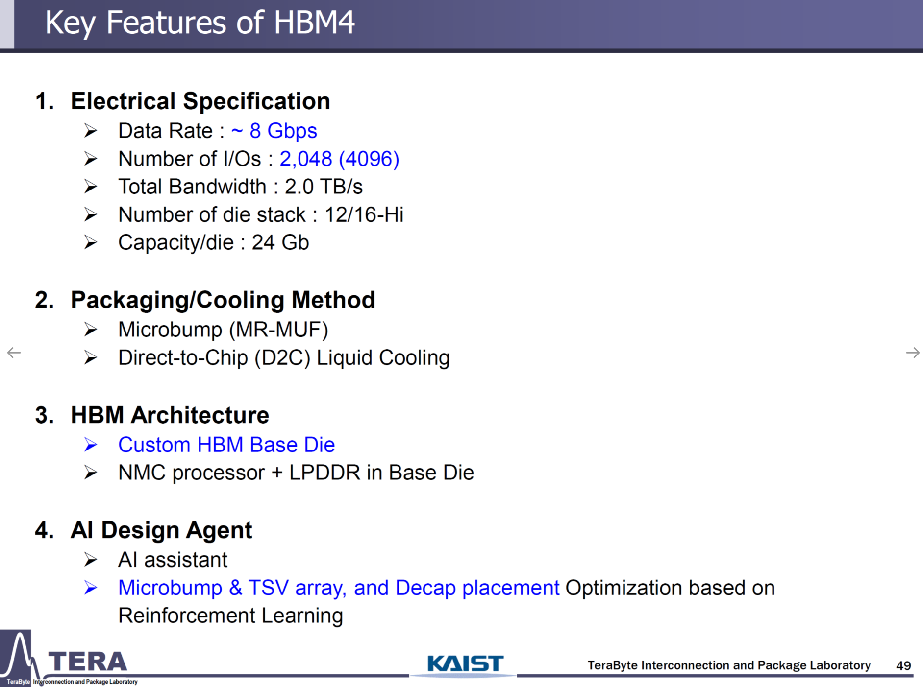
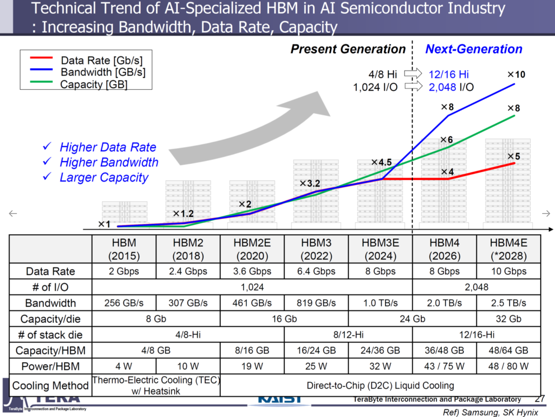
- Specifications: 8Gbps (HBM4e: 10Gbps), 2048 I/Os (up to 4096), 2.0TB/s (HBM4e: 2.5TB/s), 12/16-Hi stacks, 36/48GB per stack (HBM4e: 48/64GB), 75W (HBM4e: 80W).
- Packaging: Microbump (MR-MUF).
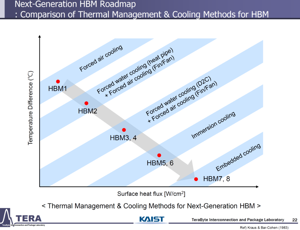
- Cooling: Direct-to-Chip (D2C) liquid cooling.
- Key Features:
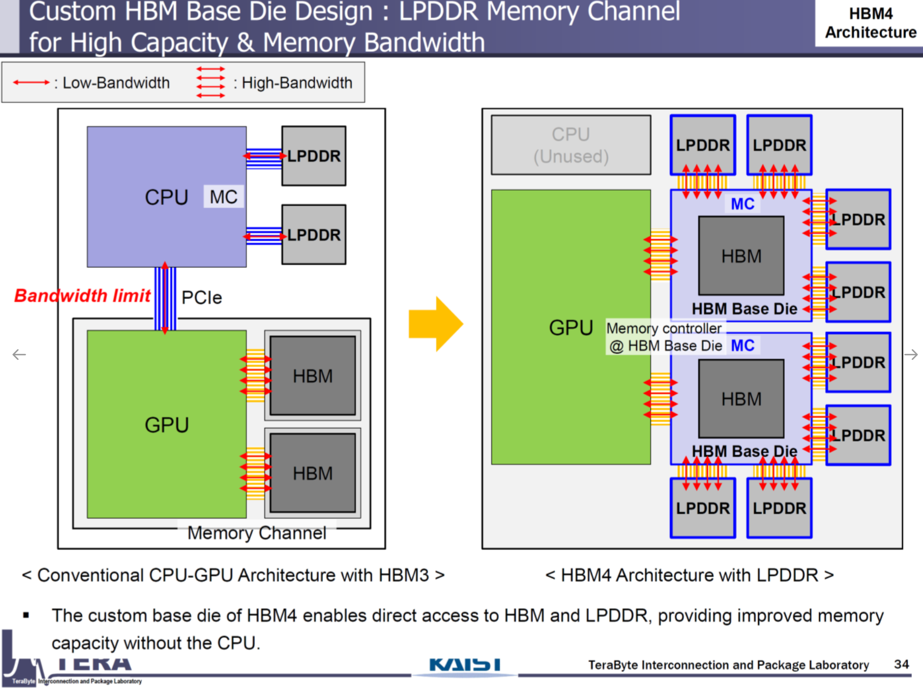
- Customized Base Die: Tailored for GPU vendors (NVIDIA, AMD, Google TPU), transitioning HBM into a system semiconductor.
- HBM-Centric Memory Network: Integrates LPDDR, acting as a memory traffic controller, reducing CPU/GPU dependency.
- Applications: NVIDIA Rubin (8 HBM4 sites, 288–384GB, 16–32TB/s), AMD MI400 (432GB, 19.6TB/s).
- Implications: HBM4 sets the stage for vendor-specific optimization, with Samsung and SK Hynix leveraging foundry and packaging expertise to capture market share.
HBM5 (2029, NVIDIA Feynman)
- Specifications: 8Gbps, 4096 I/Os, 4.0TB/s, 16-Hi stacks, 80GB per stack, 100W.
- Packaging: Microbump (MR-MUF).
- Cooling: Immersion cooling, thermal through-silicon vias (TTVs), thermal bonding.
- Key Features:
- Near-Memory Computing (NMC): Base die hosts GPU functions (e.g., floating-point, compression).
- Top-Tier Computing Die: Relocates compute to the stack’s top for enhanced cooling.
- CXL/LPDDR Integration: Expands memory network scalability.
- Thermal Vias: TTVs occupy ~30% of die area, prioritizing heat dissipation.
- Implications: HBM5’s focus on thermal management and compute integration positions it as a critical enabler for Feynman (8 HBM5 sites, 400–500GB, 4400W TDP), with cooling and TSV design defining competitive differentiation.
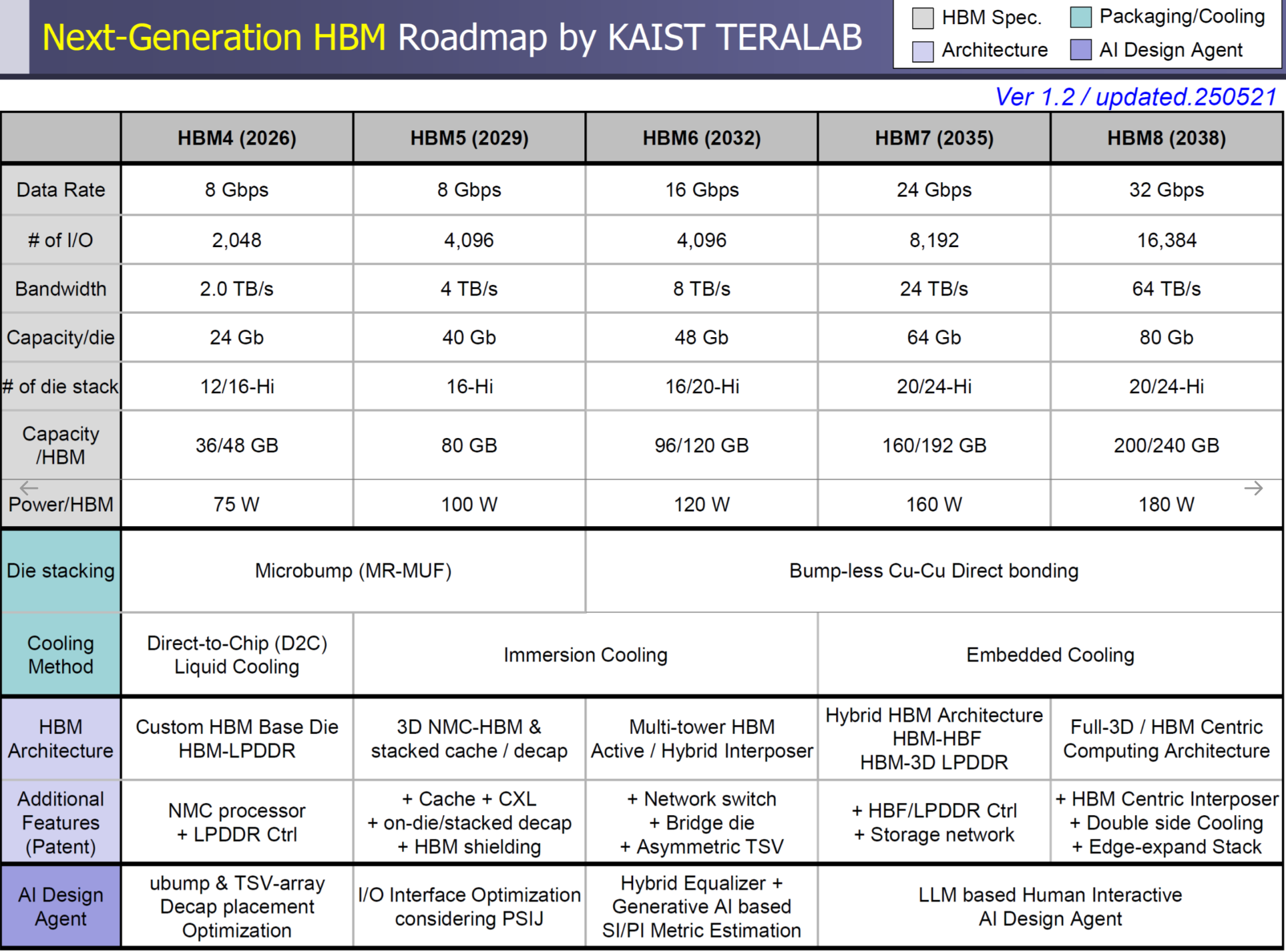
HBM6 (2032, Post-Feynman)
- Specifications: 16Gbps, 4096 I/Os, 8.0TB/s, 16/20-Hi stacks, 96/120GB per stack, 120W.
- Packaging: Bumpless Cu-Cu direct bonding.
- Cooling: Immersion cooling.
- Key Features:
- Multi-Tower HBM: Multiple HBM stacks per base die, maximizing capacity and bandwidth.
- Hybrid Interposer: Silicon+glass with through-glass vias (TGVs).
- Skybridge Interposer: Top-tier compute and cooling integration.
- Backside PDN: Enhances power delivery.
- Implications: HBM6’s hybrid interposer and multi-tower design support massive scalability (16 HBM6 sites, 1536–1920GB, 128–256TB/s), but glass interposer fabrication remains a supply chain challenge.
HBM7 (Early 2030s)
- Specifications: 24Gbps, 8192 I/Os, 24.0TB/s, 20/24-Hi stacks, 160/192GB per stack, 160W.
- Packaging: Bumpless Cu-Cu direct bonding.
- Cooling: Embedded cooling.
- Key Features:
- HBM-HBF Architecture: Integrates NAND-based High Bandwidth Flash (HBF, 1TB/stack, 4096GB/s interconnect).
- HBM-LPDDR: Low-power memory integration for edge AI.
- Network Switch: HBM manages memory traffic autonomously.
- Implications: HBM7’s embedded cooling and HBF integration enable petabyte-scale bandwidth (32 HBM7 sites, 1024TB/s, 5120–6144GB), redefining data center architectures.
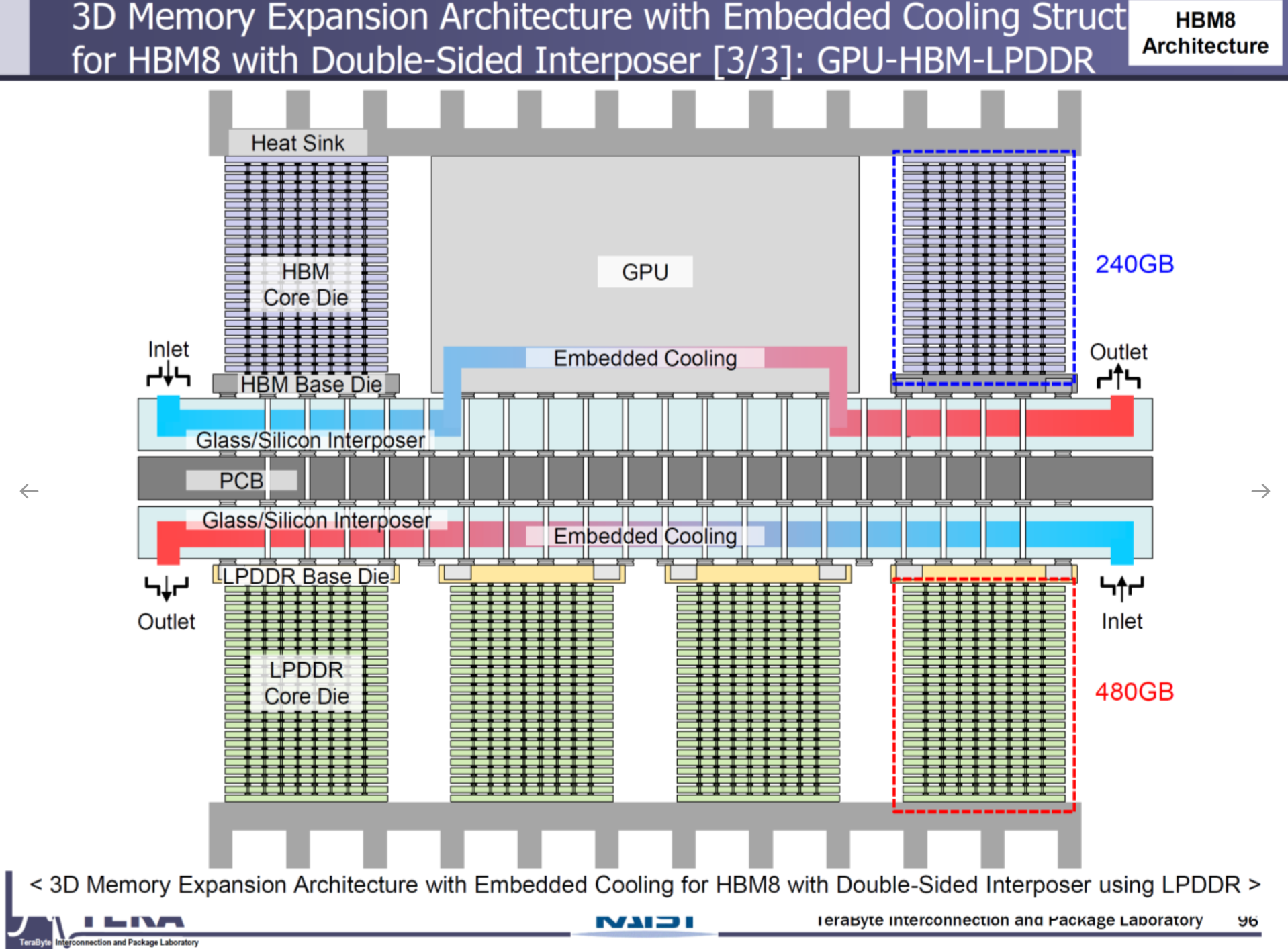
HBM8 (2038)
- Specifications: 32Gbps, 16384 I/Os, 64.0TB/s, 20/24-Hi stacks, 200/240GB per stack, 180W.
- Packaging: Bumpless Cu-Cu direct bonding.
- Cooling: Embedded cooling.
- Key Features:
- HBM-Centric Computing: HBM assumes primary compute roles, marginalizing CPU/GPU.
- Coaxial TSVs: Reduces noise for ultra-high-speed signaling.
- Optical Interconnects: HBM-to-HBM communication via photonics.
- Dual-Sided Interposer: HBM/HBF on both GPU sides.
- Implications: HBM8’s full-3D integration and optical interconnects deliver unprecedented performance, positioning HBM as the computational core for AGI/ASI.
Strategic and Technical Challenges
- Bandwidth Scaling: I/O count doubles per generation (2048 → 16384), with optical interconnects needed beyond 100Gbps.
- Capacity Expansion: 24-Hi stacks and HBF (1TB/stack) support trillion-parameter models.
- Thermal Management: Transition from D2C to embedded cooling, with TTVs and liquid channels integrated into silicon.
- Packaging Innovation: Cu-Cu bonding reduces TSV pitch to <10μm, but thermal expansion and yield remain hurdles.
- Power Delivery: Rising power (75W → 180W/stack) demands backside PDN and dynamic thermal sensors.
- HBM-Centric Paradigm: HBM’s evolution into a compute hub requires new instruction sets and software stacks.
Industry Implications
- Samsung/SK Hynix: Leadership hinges on mastering Cu-Cu bonding, embedded cooling, and HBF integration. HBM4 customization and HBM5–HBM6 thermal/TSV design are critical inflection points.
- TSMC and Competitors: TSMC’s CoWoS packaging strengthens its role, but Micron’s HBM4e entry intensifies competition.
- Supply Chain: Opportunities in TSV drilling, glass interposers, and cooling solutions for equipment vendors.
- Geopolitical Stakes: HBM underpins AI supercomputing, making it a linchpin for national security and economic competitiveness.
Conclusion
The HBM4–HBM8 roadmap redefines memory as the cornerstone of AI compute, evolving from a bandwidth enabler to a computational hub. With bandwidth scaling to 64TB/s, capacities reaching 240GB/stack, and innovations like embedded cooling and HBM-centric computing, HBM will drive the AGI/ASI era. For industry leaders, securing technological and supply chain dominance—particularly in cooling, packaging, and HBF integration—will determine market leadership over the next decade.
References: KAIST HBM Roadmap Presentation (June 16, 2025), industry analyses (H. Muztaba, June 14, 2025). Further details available upon request.