Memory Hierarchy, the Memory Wall, and the Pivotal Role of Memory Semiconductors
Introduction
The memory hierarchy is a cornerstone of modern computer architecture, enabling systems to balance the competing demands of speed, capacity, and cost. From ultra-fast registers to high-capacity hard disk drives (HDDs), each level of the hierarchy is optimized for specific performance characteristics. However, the growing disparity between processor and memory speeds—known as the memory wall—poses a significant challenge to system performance, particularly in data-intensive applications like artificial intelligence (AI), high-performance computing (HPC), and big data analytics. As the semiconductor industry evolves, memory semiconductors are becoming increasingly critical, driving innovations in high-bandwidth memory (HBM), 3D-stacked DRAM, and emerging non-volatile memory technologies. This newsletter, tailored for VLSI professionals (bachelor’s, master’s, PhD, and 10-20-year industry experts), provides a comprehensive analysis of the memory hierarchy, the memory wall, and the strategic importance of memory semiconductors in shaping the future of computing.
The Memory Hierarchy: Structure and Speed Differentials
Overview
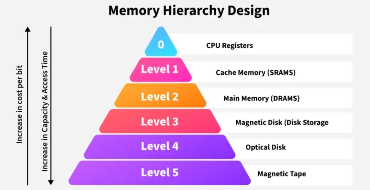
The memory hierarchy organizes storage systems into a tiered structure, leveraging the principles of temporal locality (recently accessed data is likely to be accessed again soon) and spatial locality (data near recently accessed data is likely to be accessed). This hierarchy spans multiple levels, each with distinct speed, capacity, cost, and technological characteristics. The following table summarizes the key tiers of the memory hierarchy, based on 2025-era technology:
| Memory Type | Access Time | Capacity | Cost (per GB) | Technology |
|---|---|---|---|---|
| Registers | ~0.25 ns (1 cycle, 4GHz CPU) | Hundreds of bytes | Thousands of dollars | Flip-flops |
| L1 Cache | ~1-2 ns | 32-64 KB/core | Hundreds of dollars | 6T SRAM |
| L2 Cache | ~5-10 ns | 256 KB-1 MB/core | Hundreds of dollars | 6T SRAM |
| L3 Cache | ~20-30 ns | 10-50 MB (shared) | Hundreds of dollars | 6T SRAM |
| Main Memory (DRAM) | ~100-200 ns | 16-128 GB | $5-10 | 1T1C DRAM |
| SSD | ~10-100 μs | 256 GB-4 TB | $0.1-0.5 | Flash Memory |
| HDD | ~5-10 ms | 1-16 TB | $0.02-0.03 | Magnetic Disk |
*Access time/Capacity/Cost/Technology: Just an example.
Sources: Access times are derived from Skylake processor data (Alibaba Cloud) and Meteor Lake DRAM measurements (Chips and Cheese), with adjustments for 2025 technology trends.
Speed Differentials: Root Causes
The significant variation in access times across the memory hierarchy stems from several factors, including physical proximity, memory technology, and access mechanisms. Below, we analyze each level in detail from a VLSI perspective.
Registers
- Technology: Implemented as flip-flops, typically using two cross-coupled latches to store a single bit.
- Speed: Access time is approximately one CPU clock cycle (e.g., 0.25ns at 4GHz), as registers are integrated directly into the CPU’s execution units.
- VLSI Considerations: Flip-flops require significant die area and power due to their complex transistor layout, limiting capacity to hundreds of bytes. High-speed operation is achieved through optimized transistor sizing and minimal interconnect delays.
- Constraints: High cost and area inefficiency restrict their use to critical data, such as instruction operands and temporary computation results.
Cache Memory (SRAM)
- Technology: Built using 6T SRAM cells, consisting of two cross-coupled inverters and two access transistors per bit.
- Speed:
- L1 Cache: 1-2ns, achieved through small size (32-64 KB/core), high parallelism, and proximity to CPU cores. Skylake measurements indicate 1.61ns for L1 (Alibaba Cloud).
- L2 Cache: 5-10ns, due to larger size (256 KB-1 MB) and increased tag lookup overhead.
- L3 Cache: 20-30ns, as it is shared across cores, requiring longer interconnects and more complex arbitration.
- VLSI Considerations:
- SRAM cells are area-intensive due to the 6T structure, posing scaling challenges in advanced nodes (e.g., 3nm or 2nm FinFET/GAAFET processes).
- Cache performance relies on low-latency sense amplifiers and parallel tag lookup circuits. Advanced prefetching and associativity (e.g., 8-way set-associative L1) further reduce effective latency.
- Constraints: High cost (hundreds of dollars per GB) and low density limit SRAM to small capacities, necessitating careful cache management.
Main Memory (DRAM)
- Technology: Uses 1T1C (1 transistor, 1 capacitor) cells, storing bits as charge in capacitors.
- Speed: Access time is 100-200ns, driven by:
- Row Activation: Activating a row to load data into sense amplifiers (Row Address Strobe, RAS, latency).
- Column Selection: Selecting a column for data access (Column Address Strobe, CAS, latency, e.g., 10ns for DDR4-3200 CL16 (CGDirector)).
- Refresh Cycles: Periodic refreshing (every ~50ms) to counter charge leakage, adding overhead.
- VLSI Considerations:
- The 1T1C structure enables high density (4-6x higher than SRAM), but sense amplifier sensitivity and refresh circuitry increase latency.
- DDR5 improves bandwidth (up to 4.8GT/s) but CAS latency remains high (30-40 cycles, Corsair).
- Scaling below 10nm is challenging due to capacitor size reduction and leakage issues.
- Constraints: Volatility and refresh requirements limit speed, while off-chip placement introduces interconnect delays.
Secondary Storage
- Solid-State Drives (SSD):
- Technology: Flash memory based on floating-gate transistors, storing bits as trapped charge.
- Speed: Access time is 10-100μs, driven by charge sensing for reads and electron tunneling for writes (GitHub Latency).
- VLSI Considerations: 3D NAND stacking increases density but not speed, as charge movement is physically limited. Controller overhead and block-based access further increase latency.
- Hard Disk Drives (HDD):
- Technology: Magnetic disks with mechanical read/write heads.
- Speed: Access time is 5-10ms, dominated by seek time (head movement) and rotational latency (disk spin) (GitHub Latency).
- VLSI Considerations: HDDs rely on mechanical systems, not semiconductor technology, limiting speed improvements.
Access Mechanisms and Organization
- Registers: Direct addressing with no lookup overhead, enabling sub-nanosecond access.
- Cache Memory: Set-associative organization with parallel tag lookup and data access. Hardware prefetchers predict and preload data, reducing effective latency (Alibaba Cloud).
- DRAM: 2D array with row-column addressing. Multi-bank and multi-channel designs improve parallelism, but sequential row activation and CAS latency remain bottlenecks (Wikipedia CAS Latency).
- SSD/HDD: Block-based access (pages for SSD, sectors for HDD) introduces overhead, as small data requests require reading entire blocks.
Process Technology Impact
- FinFET/GAAFET: Advanced nodes (3nm, 2nm) enable faster SRAM and register switching but constrain cache size due to area costs.
- DRAM Scaling: Sub-10nm DRAM faces challenges in maintaining capacitor charge and increasing sense amplifier latency.
- 3D NAND: Flash memory benefits from vertical stacking, but speed is limited by electron tunneling physics.
The Memory Wall: A Growing Challenge
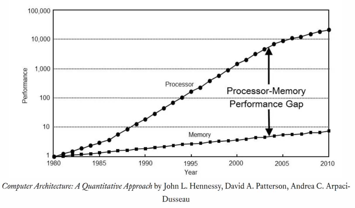
The memory wall, first identified in the 1990s, describes the performance bottleneck caused by the divergence between processor and memory speeds. While CPU performance has scaled with Moore’s Law (doubling transistor counts every ~2 years), memory access times have improved far more slowly. For example:
- CPU: Modern CPUs operate at 5GHz+, with single-cycle register access (~0.2ns).
- DRAM: Access times remain at 100-200ns, a gap of 2-3 orders of magnitude (Chips and Cheese).
Impact
- AI and HPC: AI training requires massive data throughput, but DRAM latency limits GPU/TPU performance. For instance, NVIDIA’s H100 GPU relies on HBM3E to mitigate this (Samsung HBM).
- Big Data: Analytics workloads involve frequent memory accesses, exacerbating the bottleneck.
- Energy Efficiency: Data movement between CPU and memory consumes significant power, a critical concern in data centers.
Mitigation Strategies
To address the memory wall, the semiconductor industry is pursuing several approaches:
- High-Bandwidth Memory (HBM): 3D-stacked DRAM with through-silicon vias (TSVs) offers up to 1.23TB/s bandwidth (HBM3E, Rambus HBM3E). SK Hynix’s 16-layer HBM3E achieves 18-32% performance gains in AI tasks (TrendForce SK Hynix).
- Processing-in-Memory (PIM): Performs computations within memory, reducing data movement. Samsung’s PIM-enabled HBM doubles performance and cuts energy use by 70% (Wikipedia HBM).
- Compute-in-Memory (CIM): Integrates logic directly into memory arrays, ideal for AI inference.
- 3D-Stacked DRAM: Increases density and bandwidth via TSVs and chiplet designs (Imec VLSI 2025).
- Non-Volatile Memory: MRAM, ReRAM, and PCM offer low latency and non-volatility, bridging the gap between DRAM and flash (Wevolver HBM).
- Storage-Class Memory (SCM): Intel’s 3D XPoint (Optane) combines DRAM-like speed with flash-like persistence (TechTarget HBM).
- Cache Optimization: Larger L3 caches (e.g., 50MB in modern CPUs) and advanced prefetching improve hit rates.
- Interconnect Improvements: CXL (Compute Express Link) and high-bandwidth interconnects reduce off-chip latency.
The Critical Role of Memory Semiconductors
Driving Forces
Memory semiconductors are increasingly central to the semiconductor industry due to several trends:
- AI and Machine Learning: AI models (e.g., large language models) require massive memory bandwidth and low latency. HBM3E and HBM4 are critical for GPUs and AI accelerators (Samsung HBM).
- Big Data and IoT: The explosion of data from IoT devices and analytics platforms demands high-capacity, high-speed memory.
- 5G and Edge Computing: Edge devices require low-power, high-performance memory for real-time processing.
- Energy Efficiency: Data centers, consuming ~1% of global electricity, prioritize memory technologies that reduce power usage (Bloomberg HBM Market).
Key Innovations
- HBM: SK Hynix and Samsung lead HBM3E and HBM4 development, with SK Hynix targeting HBM4 mass production in 2025 (TrendForce SK Hynix). HBM’s 1024-bit bus and 1.23TB/s bandwidth make it ideal for AI and HPC.
- 3D DRAM: Research at the 2025 VLSI Symposium highlights 3D DRAM for higher density and bandwidth (Imec VLSI 2025).
- Non-Volatile Memory:
- MRAM: Fast, durable, and non-volatile, suitable for cache replacement.
- ReRAM: High density and low power, ideal for storage-class memory.
- PCM: Phase-change memory for scalable, persistent storage.
- PIM and CIM: These paradigms shift computation to memory, reducing latency and power. Samsung’s PIM-HBM is a notable example (Wikipedia HBM).
- CFET-Based SRAM: Complementary FETs (CFETs) enable SRAM scaling in sub-2nm nodes, as presented at VLSI 2025 (Imec VLSI 2025).
- SCM: 3D XPoint bridges DRAM and flash, offering intermediate latency and persistence (TechTarget HBM).
Market Outlook
The HBM market is projected to grow from $4 billion in 2023 to $130 billion by 2033, with a 42% CAGR (Bloomberg HBM Market). SK Hynix has nearly sold out its 2025 HBM production, underscoring demand (Reuters SK Hynix). The broader memory semiconductor market, including DRAM and NAND, is expected to exceed $200 billion by 2030, driven by AI and data center growth.
Challenges
- Cost: HBM’s complex manufacturing (e.g., TSVs, 3D stacking) results in high costs ($25-35/GB vs. $5-10/GB for DDR5).
- Thermal Management: 3D-stacked memory generates significant heat, requiring advanced cooling solutions.
- Yield: HBM3E yield has improved to ~80% (TrendForce SK Hynix), but scaling to HBM4 remains challenging.
- Scaling Limits: DRAM and SRAM face physical limits below 10nm, necessitating new materials and architectures.
Future Directions
The semiconductor industry is shifting toward memory-centric architectures to meet future demands:
- Heterogeneous Integration: Chiplets and 3D packaging enable modular memory designs with improved bandwidth and flexibility.
- Neuromorphic Computing: Memory-intensive architectures inspired by the human brain require low-latency, high-density memory.
- Quantum Computing: Emerging quantum systems may leverage non-volatile memory for error correction and state storage.
- Sustainability: Low-power memory technologies (e.g., MRAM, PIM) are critical for reducing the environmental impact of data centers.
Conclusion
The memory hierarchy is a fundamental framework for optimizing computer performance, but the memory wall poses a significant challenge as processor speeds outpace memory advancements. Memory semiconductors, from HBM and 3D DRAM to emerging non-volatile technologies, are critical to overcoming this bottleneck and enabling the next generation of computing. For VLSI professionals, understanding the interplay of memory technologies, process advancements, and system-level innovations is essential. The 2025 VLSI Symposium’s focus on 3D DRAM and CFET-based SRAM underscores the industry’s commitment to addressing these challenges. As AI, big data, and edge computing continue to drive demand, memory semiconductors will remain at the forefront of technological innovation, shaping the future of the semiconductor industry.
Key Citations
- Memory Hierarchy Design and Characteristics
- Latency Numbers Every Programmer Should Know
- Meteor Lake DRAM Latency Measurements
- Measuring Cache Access Latency Mechanism
- CAS Latency in DDR5 Explained
- RAM Latency Guide and Importance
- HBM3E: Everything You Need to Know
- SK Hynix to Showcase 16-layer HBM3E Samples at CES 2025
- SK Hynix Revealed Progress for HBM3e, Achieving Nearly 80% Yield
- High Bandwidth Memory Chip Market to Grow to $130 Billion by 2033
- High Bandwidth Memory
- 2025 Symposium on VLSI Technology and Circuits
- High Bandwidth Memory: Concepts, Architecture, and Applications
- What is High Bandwidth Memory?