What is 'Clock mesh' in Physical Design?

In digital semiconductors, the most critical signal is the clock.
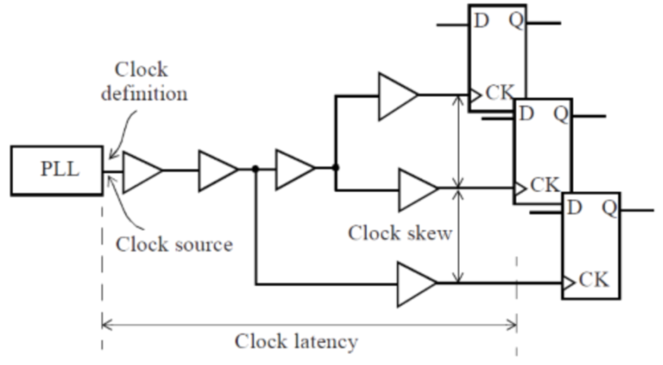
The delay from the clock source to the clock pin of a sequential cell is called Clock Latency.
The difference in latency between sequential cells is referred to as Clock Skew.
From Zero Skew to Useful Skew
In the past, the goal of Clock Synthesis was to achieve zero skew — to align all clock arrivals perfectly.
This made chip signoff much simpler.
However, as chip complexity grew, the number of cells increased dramatically, leading to power, performance, and area (PPA) challenges.
Various Clock Tree structures, such as H-Tree and Fishbone, were introduced to mitigate these issues.
Yet even with those methods, achieving zero skew proved difficult.
Thus, modern designs began to intentionally apply Useful Skew — deliberately adjusting clock arrival times to optimize timing.
The Classic Clock Tree
Historically, the clock network was synonymous with the term “Tree” —
a unidirectional structure that starts from the root, branches out, and finally reaches the leaf nodes.
This is called a Single Source Clock Tree (SSCT).
It offered relatively simple prediction of clock skew and delay.
In a Clock Tree structure, the buffer at the very top acts as the clock source, and its waveform propagates downward.
Because each sink point is located differently, the number of buffers along each path varies — leading to differences in total latency and, consequently, skew.
The Challenge at Advanced Nodes
As semiconductor processes entered the 7nm and below era, the situation changed drastically.
Process variation and wire RC delay became dominant factors.
With these variations, a purely unidirectional tree structure could no longer control skew within just a few picoseconds.
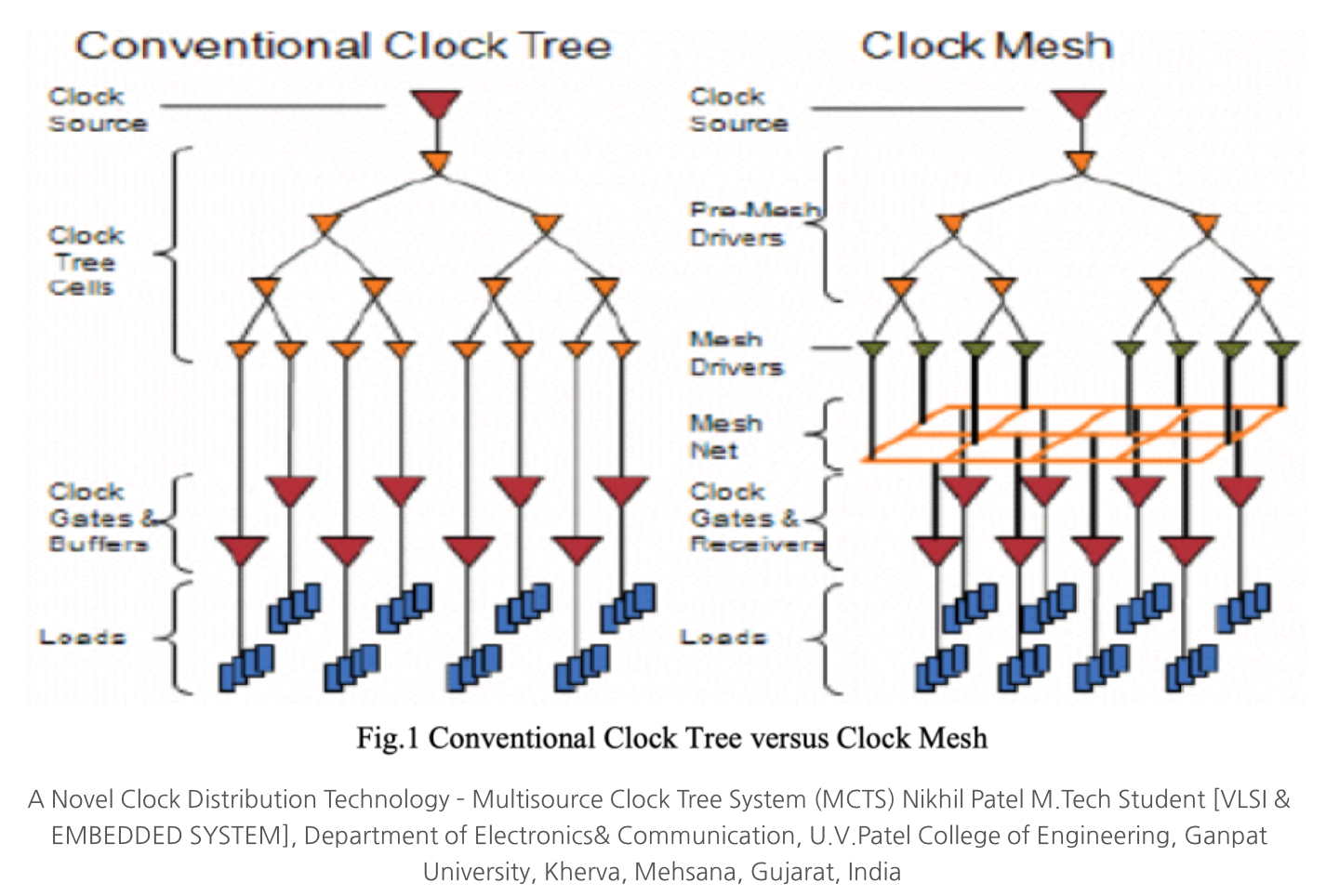
The Emergence of the Clock Mesh
This limitation led to the development of the Clock Mesh architecture.
In a mesh, numerous metal lines are arranged horizontally and vertically, forming a grid where every node is electrically connected.
Imagine the sink pins are far apart:
- Conventional Tree Method: Latency differences between sequential cells accumulate along the path from source to sink.
- Mesh Method: Within the mesh, latency differences are effectively canceled out.
As a result, Clock Mesh achieves much smaller skew than traditional trees.
Structure and Concept of Clock Mesh
At its core, a Clock Mesh is a redundant and averaged distribution network.
The typical structure works as follows:
- At the upper level, multiple clock drivers (buffers) simultaneously drive the mesh grid.
- Each node in the grid is connected by metal lines, so delay variation becomes averaged out across the network.
- The leaf flops connect to various nodes within the mesh.
Unlike a digital-only perspective, Clock Mesh should be understood through analog electrical behavior.
The Principle: Electrical Averaging
In a mesh, all nodes are electrically connected through resistive (R) and capacitive (C) metal networks.
When one driver’s voltage begins to swing first, its node pushes current through the resistive paths to neighboring nodes.
The neighboring (slower) nodes receive this current, causing them to rise faster.
Meanwhile, the faster node slows slightly due to resistive loss.
This short-term current exchange pulls the transition timings closer together, a phenomenon known as Electrical Averaging.
Effectively, the metal mesh acts like a spatial low-pass filter, quickly reducing voltage differences across coordinates — resulting in tightly aligned arrival times.
Trade-offs and Practical Usage
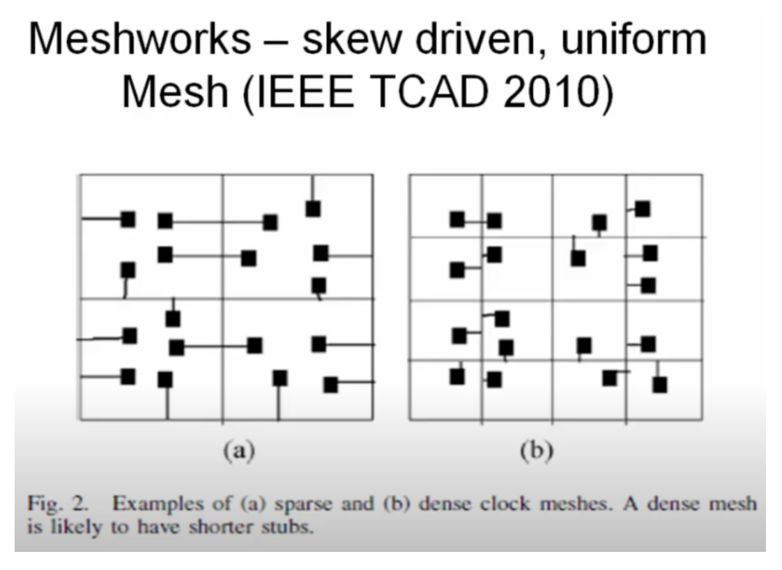
However, as the mesh becomes denser and wider, the total wire length, power, and area increase.
Analysis complexity also grows for STA, EM, IR drop, and parasitic extraction/simulation.
Therefore:
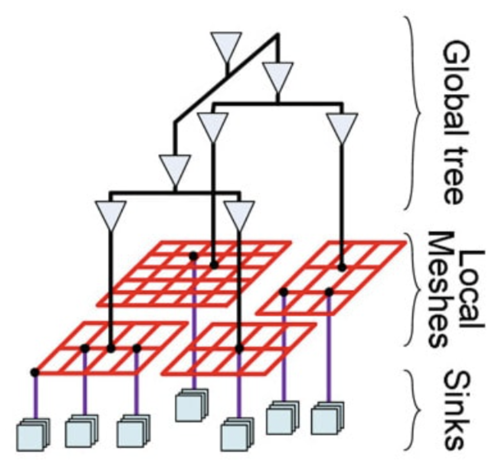
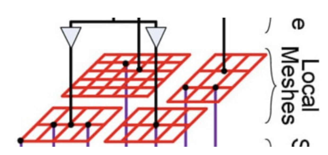
- High-performance cores often use Mesh or Tree + Local Mesh (Hybrid) structures.
- Mobile or low-power SoCs typically rely on well-balanced tree designs for efficiency.
Thanks to the resistive connections in the metal grid, faster nodes feed current into slower ones, causing both transitions to converge.
This RC-network electrical averaging is what dramatically reduces skew compared to a pure tree structure.
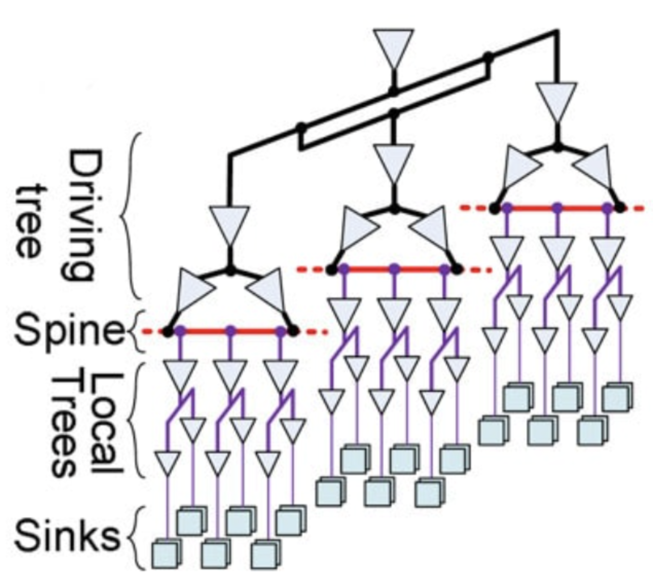
Hybrid Clock Mesh and Multi-Point CTS
A full mesh consumes a large amount of metal wiring, leading to excessive area and power overhead — especially problematic for DFT integration.
If the mesh spacing is too coarse, long nets can cause violations, so dense meshing is required.
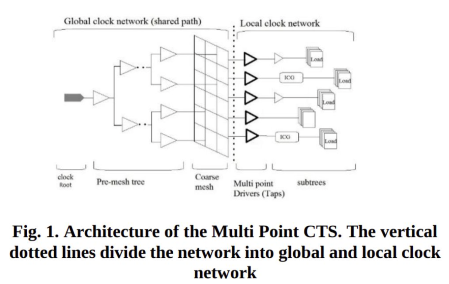
To balance skew control and efficiency, the industry now favors the Hybrid Clock Mesh, also known as Multi-Point CTS (Clock Tree Synthesis).
This hybrid approach combines traditional CTS and clock mesh techniques:
- Build a minimal pre-mesh region.
- Drive the mesh with a limited number of multi-point driver taps.
- Each tap then distributes the clock downstream through a tree-like network.
The global mesh resides in the chip’s upper metal layers, forming a coarse mesh to minimize global skew,
while local trees distribute the clock within subregions.
This hybrid architecture guarantees smaller skew than pure trees while controlling the power and area costs that come with a full mesh — making it the dominant solution in modern industry.