VLSI Korea
Daily Silicon: Marvell $2.739B: AI Silicon Design and GAA
A practicing semiconductor engineer's daily read on global silicon news - Marvell $2.739B: AI Silicon Design and GAA


🆓 무료 글 · 누구나 무료로 읽을 수 있는 글입니다
A practicing semiconductor engineer's daily read on global silicon news:
Marvell's FY2027 Q2 revenue rose 37% to $2.739B and Data Center revenue grew 46%; today's constraint is not GPU count but closing custom-silicon qualification, HBM packaging, and GAA process variation on the same schedule.
Chase's Take - I do not read Marvell's $3.150B guidance as a simple AI-demand indicator. Even after RTL signoff, custom silicon turns into revenue only when SerDes, package substrate, HBM sourcing, board bring-up, and customer qualification all close in the same window.
The next checkpoint is the October 6, 2026 Investor Day, where I want to see how Custom and Connectivity ramp timing maps to wafer starts and packaging slots.
1. Marvell FY2027 Q2 Results: Transition to Custom Silicon
TL;DR - Marvell posted $2.739B in FY2027 Q2 and guided Q3 to $3.150B.
Production-qualification speed, not design wins, now gates revenue conversion.
Source: Marvell Technology - Marvell FY2027 Q2 Results: Transition to Custom Silicon
2. SK hynix Indiana HBM Production Base: Korean Wafers, U.S. Packaging
TL;DR - SK hynix will invest over $4 billion in an advanced HBM packaging fab in Indiana, targeting mass production in the second half of 2029.
Source: SK hynix - SK hynix Indiana HBM Production Base: Korean Wafers, U.S. Packaging
3. Lam Research Breaks Ground on Oregon Lab for AI-Era Semiconductor R&D
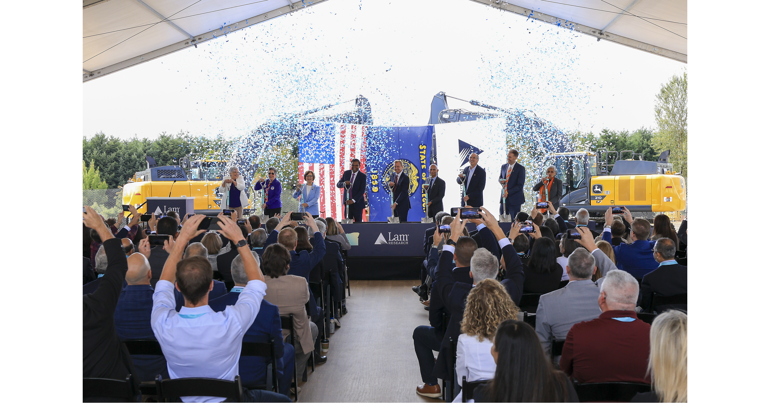
TL;DR - Lam Research broke ground on a 120,000 square foot Oregon lab, the first step in over $3 billion of global lab-network expansion over five years.
Source: Lam Research - Lam Research Breaks Ground on Oregon Lab for AI-Era Semiconductor R&D
4. GAA Channel Non-Uniformity: 4nm to 7nm Top Channel

TL;DR - Lam's SEMulator3D model shows nFET stacked-nanosheet stress difference can reach 400-800 MPa and falls when the top channel grows from 4nm to 7nm.
Source: Lam Research - GAA Channel Non-Uniformity: 4nm to 7nm Top Channel
What to Watch Next
- Marvell Investor Day, October 6, 2026
It will show how tightly Custom and Connectivity ramp timing aligns with wafer starts, substrate, and packaging slots. - SK hynix Indiana cleanroom completion target, October 2028
HBM supply must be judged by the simultaneous ramp of U.S. packaging, test, and customer qualification, not wafers alone. - Process correlation between per-stack GAA stress and Vt distribution
Even with favorable average device metrics, the top-channel leakage tail can set guardband and yield. - Progress toward opening Lam's Oregon lab in 2028
Advanced-node equipment learning cycles are bounded by cleanroom experiment capacity and metrology feedback.
Signal Radar - More Headlines
- Hybrid Bonding: Foundational Technology for Semiconductor Performance (SK hynix)
- Advantest to Present Latest Test Solutions at SEMICON Taiwan 2026 (Advantest)
- 2026 World Climate Expo (WCE) Notice (Korea Semiconductor Industry Association)
- Relevant Ministries Join Forces to Build a Robust Industrial and Technology Security Network (Ministry of Trade, Industry and Energy)
- Forum Launches to Strengthen Testing and Certification Industry Competitiveness (Ministry of Trade, Industry and Energy)
- [Embassy of the Republic of Korea in India] India Semiconductor Mission (ISM) 2.0 Webinar Announcement (Korea Semiconductor Industry Association)
- 2026 JEDEC FORUM (Korea Semiconductor Industry Association)
- [3M] Semiconductor Personal Protective Equipment White Paper and Survey Notice (Korea Semiconductor Industry Association)
- [Bae, Kim & Lee LLC] Seminar on Semiconductor Export-Control Issues and Corporate Response Strategies in Korea and the U.S. (Korea Semiconductor Industry Association)
- Gwangju AI Brooklyn Square Knowledge Industry Center Demand Survey (Korea Semiconductor Industry Association)
Further Reading on VLSI Korea
- Weekly Silicon: AI Capex Is Validated Through Power, HBM, and Custom Silicon
A deeper read on the background to today's brief. - What Is a Post-CMP Cleaner? The Defect Contract That Closes Particle Removal and Metal Corrosion Together
A deeper read on the background to today's brief.
Frequently Asked Questions
What did Marvell report for FY2027 Q2?
Marvell posted FY2027 Q2 revenue of $2.739 billion, up 37%, with Data Center revenue growing 46%. Q3 guidance is $3.150 billion.
What is SK hynix building in Indiana?
SK hynix will invest over $4 billion in an advanced HBM packaging fab in Indiana. It targets mass production in the second half of 2029, with cleanroom completion targeted for October 2028.
What is Lam Research building in Oregon?
Lam Research broke ground on a 120,000 square foot Oregon lab. It is the first step in over $3 billion of global lab-network expansion over five years.
What does the GAA channel study show?
The model shows nFET stacked-nanosheet stress difference can reach 400-800 MPa. The stress falls when the top channel grows from 4nm to 7nm.
Related reading
- Daily Silicon: Semiconductor Design and AI Chips: CoWoS and $3 billion R&D
- Daily Silicon: AMAT WFE Guide to 30%+, Foxconn AI Server Surge, Hynix…
- Daily Silicon: Infineon €4.172B: AI Chip Power and Semiconductor Design
- Daily Silicon: NVIDIA $96.2B, AI Silicon and UCIe Design Shift
- Daily Silicon: Sumitomo ¥34.2B: Semiconductor Design and AI Chips