VLSI Korea
Daily Silicon: Samsung HBM4, NVIDIA CUDA: 4nm Base Die and 2nm SRAM
A practicing semiconductor engineer's daily read on global silicon news - Samsung HBM4, NVIDIA CUDA: 4nm Base Die and 2nm SRAM


🆓 무료 글 · 누구나 무료로 읽을 수 있는 글입니다
A practicing semiconductor engineer's daily read on global silicon news:
HBM4 competition is shifting from stack height to the controller, test, and telemetry placed in a 4nm base die, while CUDA on RISC-V is a server-platform qualification problem spanning PCIe coherency and peer-to-peer paths.
Chase's Take - I do not read HBM4's 4nm base die as a bandwidth headline. Once the PHY area savings go to memory controller and test, package signoff becomes joint qualification of repair maps, thermal telemetry, and host protocol, not just signal integrity.
CUDA on RISC-V has the same structure. The next check is whether the Hot Chips material turns into explicit ACPI, PCIe coherency, and peer-to-peer validation criteria for actual server platforms.
1. Hot Chips 2026: Samsung HBM Base Die Opportunities, HBM4 4nm
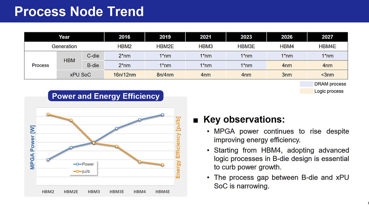
TL;DR - Samsung is moving HBM4 and HBM4E base dies to a 4nm logic node, turning PHY area and power constraints into design space for controller, repair, and telemetry functions.
Source: Chips and Cheese - Hot Chips 2026: Samsung HBM Base Die Opportunities, HBM4 4nm
2. Hot Chips 2026: CUDA Targets RISC-V, PCIe Coherency
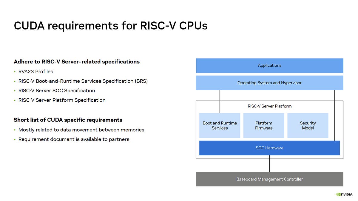
TL;DR - NVIDIA's CUDA path for RISC-V assumes a server platform with RVA23, ACPI, PCIe coherency, and peer-to-peer transfers.
Source: Chips and Cheese - Hot Chips 2026: CUDA Targets RISC-V, PCIe Coherency
3. Process-Aware Hybrid Si/IGO Monolithic-3D 6T SRAM: 25% 2nm Area Cut

TL;DR - A new monolithic-3D 6T SRAM study reports a 25% footprint reduction versus the HP baseline using BEOL IGO pass gates and Si nanosheet latches.
Source: arXiv - Process-Aware Hybrid Si/IGO Monolithic-3D 6T SRAM: 25% 2nm Area Cut
4. Micron's Boise Training Center Replicates Up to 20 Fab Tools
TL;DR - Micron will place up to 20 process tools in its 60,000-square-foot training center and expand apprenticeships to triple-digit enrollment by the end of fiscal 2027.
Source: Micron Technology - Micron's Boise Training Center Replicates Up to 20 Fab Tools
What to Watch Next
- NVIDIA and Synopsys earnings on August 26
Official guidance on AI accelerator demand and EDA backlog becomes a P0 candidate for the next Daily. - CUDA RISC-V ACPI and PCIe coherency implementation scope
The actual server-platform qualification scope must be fixed before software-port costs can be separated from silicon-validation costs. - Disclosure of controller and test functions in the HBM4 logic base die
Whether HBM retains a standard interface or moves to a custom protocol changes multi-sourcing and package validation. - Apprenticeship enrollment at the Boise training center
It will show whether operator and maintenance qualification, rather than fab-equipment supply, becomes the real ramp rate limiter.
Signal Radar - More Headlines
- HBF Adds Capacity Alongside HBM but Requires Runtime Redesign (Chips and Cheese)
- SiFive BigSky Introduces a 32-Core RVA23 Server Platform (Chips and Cheese)
- Intel Wildcat Lake Recalculates UCIe Power and BOM for Low-Cost Notebooks (Chips and Cheese)
- Multi-Die Assembly Below 2nm Raises Design and Verification Burden (Semiconductor Engineering)
- Edge AI and Cloud AI Role Separation Shifts to System Co-Optimization (Semiconductor Engineering)
- SNU and Sungkyunkwan Antiferroelectric Device Distinguishes 16 States From a 4-Bit Input (Semiconductor Engineering)
- High-Entropy Oxide Semiconductor Targets Low Thermal Conductivity (Communications Materials)
- Ultrathin Semiconductor Can Be Reprogrammed Repeatedly With Light (Princeton Engineering)
- Seoul National University Opens a Physical AI National Research Laboratory (Seoul National University)
- Hot Chips 2026 Ran at Stanford From August 23 to 25 (Semiconductor Engineering)
Further Reading on VLSI Korea
- The 256-Core Server CPU Bottleneck Is Not Core Count: Diamond Rapids' Memory-I/O Envelope
Useful background on why host-memory bandwidth and package I/O constrain compute density.
Related reading
- Daily Silicon: Samsung KRW 89.5T Profit, HBM4 and ATE Capacity
- Daily Silicon: AMD Helios: 72 GPUs, HBM4 and NVIDIA AI Chips
- Daily Silicon: TSMC Packaging Yield Hits 98% — Cracks in the Cycle Peak
- Daily Silicon: Premarket +6%, Next Inflection Points Are AMAT and NVDA…
- Daily Silicon: AMD 2nm Defects to Samsung, SK hynix Tests Intel EMIB —…
- The Cost of CUDA on RISC-V Is Platform Qualification, Not the ISA Port