VLSI Korea
Daily Silicon: AMD Helios: 72 GPUs, HBM4 and NVIDIA AI Chips
🆓 무료 글 · 누구나 무료로 읽을 수 있는 글입니다 A practicing semiconductor engineer's daily read on global silicon news: AMD is shifting AI competition to rack-scale memory and networking, while CXMT and Wistron turn capital and assembly capacity into the next supply constraints. Read this every morning at 06:00 KST. Daily Silicon is VLSI Korea’s engineer-


🆓 무료 글 · 누구나 무료로 읽을 수 있는 글입니다
A practicing semiconductor engineer's daily read on global silicon news:
AMD is shifting AI competition to rack-scale memory and networking, while CXMT and Wistron turn capital and assembly capacity into the next supply constraints.
Chase's Take - I look first at Helios's 31TB of HBM4 and 2.4Tbps of scale-out bandwidth per GPU, not its 2.9 exaflops of FP4. Compute can scale, but 72 GPUs will not behave as one resource unless package routing, retimers, switch ports, cable count, and rack power scale with it.
AMD's comparisons with NVIDIA Vera Rubin NVL72 are all internal, so I will not keep score until customer workloads expose token throughput and fabric recovery time. CXMT's RMB29.5B allocation to wafer lines, DRAM process migration, and next-generation R&D will matter at equipment ordering and customer qualification, not in its first-day share price.
For STA and backend, die-level PPA closure is no longer enough: UCIe channel compliance, package thermal maps, stack-level DFT, and aged-corner timing belong on the tapeout checklist.
1. AMD Helios Rack-Scale AI Infrastructure: 72 GPUs, 31TB HBM4
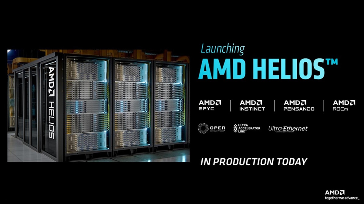
TL;DR - AMD Helios connects 72 MI455X GPUs in one scale-up domain, with 31TB of HBM4 and 1.7PB/s of aggregate HBM bandwidth.
Source: AMD - AMD Helios Rack-Scale AI Infrastructure: 72 GPUs, 31TB HBM4
2. China DRAM Maker CXMT IPO: RMB57.9B Raise on July 27
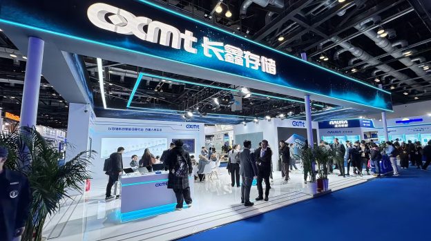
TL;DR - CXMT will list on Shanghai's STAR Market on July 27, raising RMB57.919B before over-allotment and up to RMB66.6B in total.
Source: TrendForce - China DRAM Maker CXMT IPO: RMB57.9B Raise on July 27
3. Wistron U.S.-Made GB300 Baseboard: D1 Is 5% of NVIDIA Output
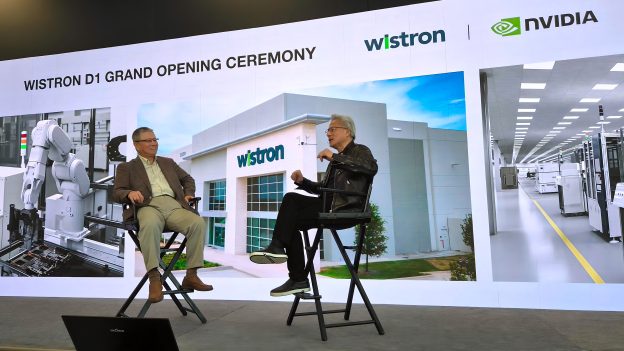
TL;DR - Wistron has started volume L6 assembly and testing of NVIDIA GB300 baseboards and AI servers at its $700M D1 plant in Fort Worth, Texas.
Source: TrendForce - Wistron U.S.-Made GB300 Baseboard: D1 Is 5% of NVIDIA Output
4. Vulcano 800 AI NIC: 2.4Tbps per GPU, 13% Shorter Job Time

TL;DR - AMD Pensando Vulcano 800 delivers 800Gbps per NIC and up to three NICs per GPU, providing 2.4Tbps of scale-out bandwidth per GPU.
Source: AMD - Vulcano 800 AI NIC: 2.4Tbps per GPU, 13% Shorter Job Time
5. Ryzen AI Embedded X100: 273GB/s and 10-Year Supply
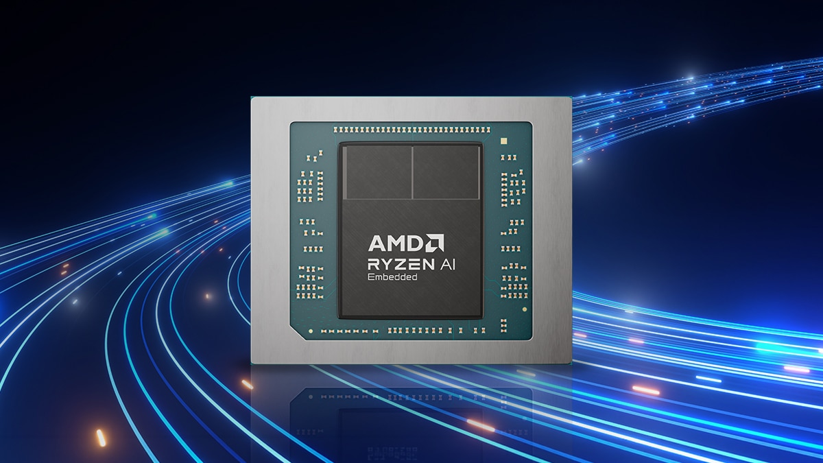
TL;DR - AMD Ryzen AI Embedded X100 shares 273GB/s unified memory and 32MB of cache across its CPU, GPU, and NPU, with a planned 10-year supply window.
Source: AMD - Ryzen AI Embedded X100: 273GB/s and 10-Year Supply
6. NVIDIA GPU-Accelerated Medical Physics: 8,192 Environments
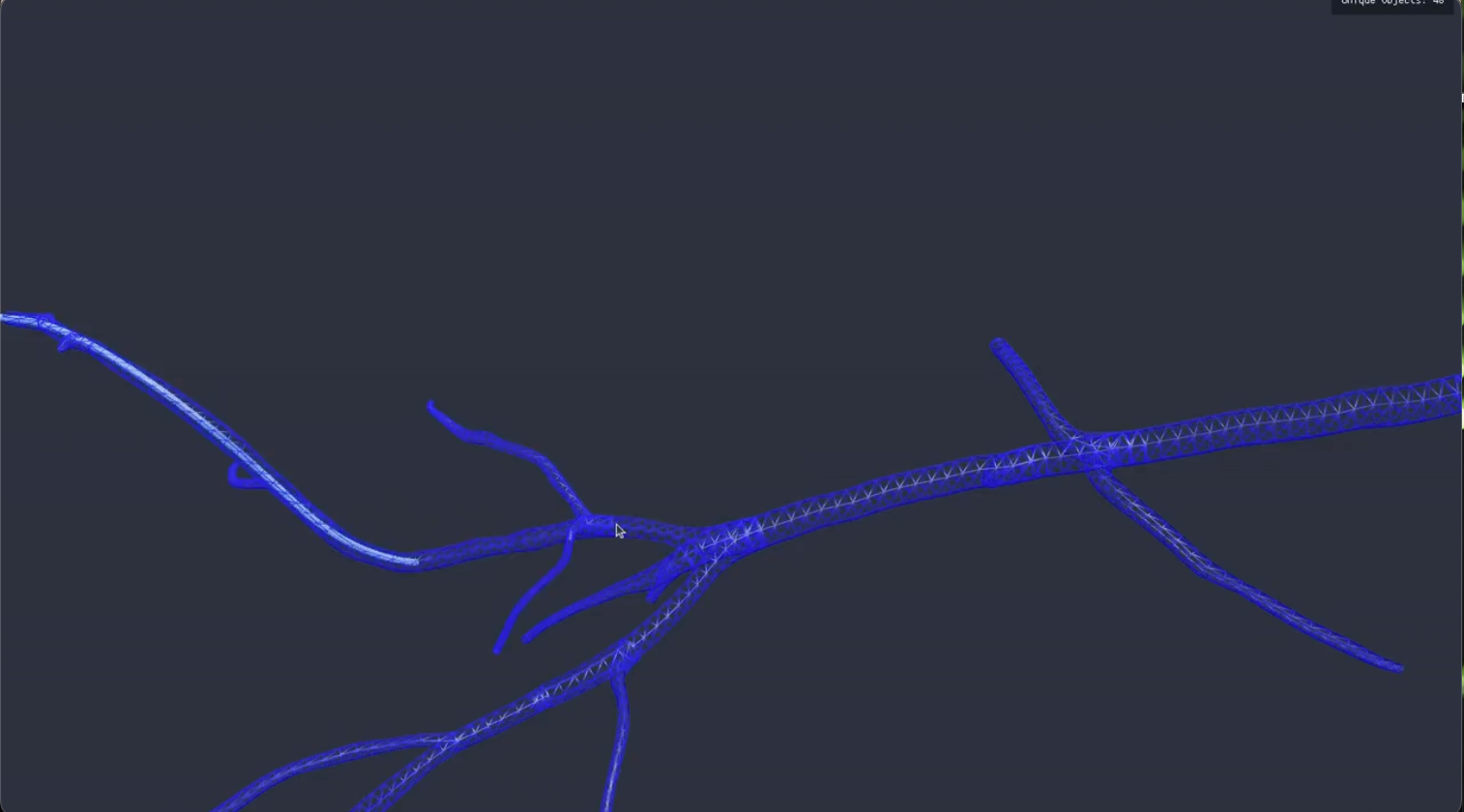
TL;DR - NVIDIA ran 8,192 robot-training environments in parallel with GPU-native medical physics simulation, cutting training time from more than five hours to under two minutes.
Source: NVIDIA - NVIDIA GPU-Accelerated Medical Physics: 8,192 Environments
7. Arm AGI CPU: About 2x Requests in an Under-40kW Rack
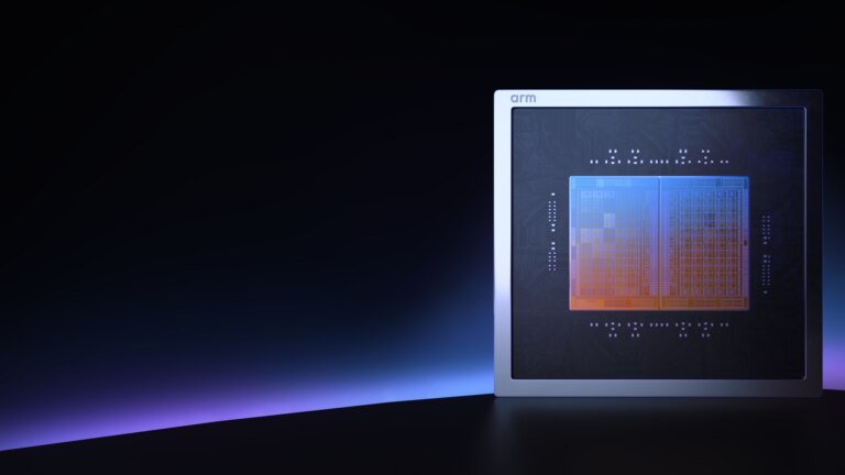
TL;DR - Arm estimates that an under-40kW AGI CPU rack paired with Rebellions accelerators handled about 2x more automated requests than a legacy x86 rack.
Source: Arm - Arm AGI CPU: About 2x Requests in an Under-40kW Rack
8. 3D-IC Final Sign-Off: Joint UCIe, Power and Thermal Verification
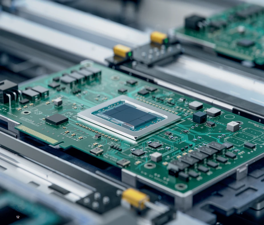
TL;DR - Thousands of connections in a multi-chiplet package require one flow spanning UCIe pre-route compliance, multiphysics, stack-level DFT, and full-assembly DRC and LVS.
Source: Semiconductor Engineering - 3D-IC Final Sign-Off: Joint UCIe, Power and Thermal Verification
9. Verification at DAC 2026: Natural-Language Test Plans and Emulation
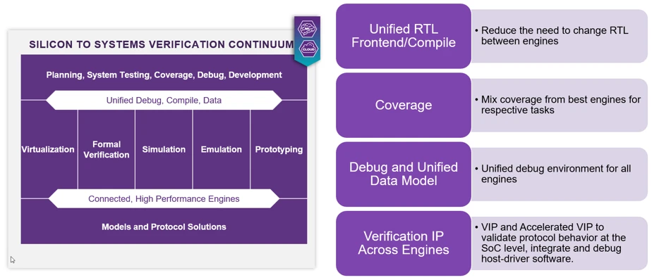
TL;DR - The verification focus at DAC 2026 is an execution flow that reuses Python and SystemVerilog test content across simulation, emulation, and FPGA prototypes.
Source: Semiconductor Engineering - Verification at DAC 2026: Natural-Language Test Plans and Emulation
10. Reliability Degradation Parameters for Design Choices: HCI and BTI
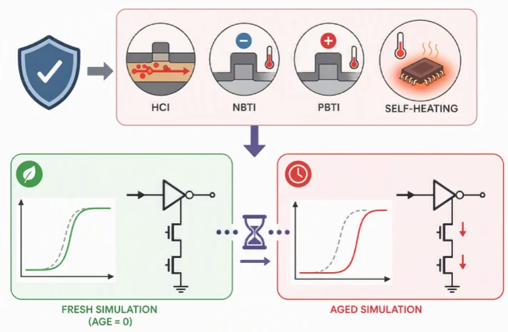
TL;DR - Cadence ADE's reliability flow connects fresh, stress, and aged simulation, then uses relxexpr to place maxima, minima, and violation counts into pass/fail specifications.
Source: Semiconductor Engineering - Reliability Degradation Parameters for Design Choices: HCI and BTI
11. Chip Policy: UK vs. U.S. vs. EU vs. India

TL;DR - U.S., EU, Indian, and UK semiconductor policies are not one subsidy race: each targets a different asset across fabs, strategic nodes, and fabless IP.
Source: Semiconductor Engineering - Chip Policy: UK vs. U.S. vs. EU vs. India
Daily Semiconductor Market Board
TradingView delayed quote basis. Click each ticker for the TradingView chart. Change uses daily change.
| Company | Ticker | Price | Daily Change |
|---|---|---|---|
| NVIDIA | NVDA | $206.84 | -0.92% |
| AMD | AMD | $521.95 | -3.29% |
| Broadcom | AVGO | $381.92 | -2.69% |
| TSMC ADR | TSM | $403.41 | -2.93% |
| ASML | ASML | $1,757.09 | -2.55% |
| Arm | ARM | $260.01 | -8.14% |
| Qualcomm | QCOM | $166.97 | -2.42% |
| Micron | MU | $920.95 | -6.99% |
| Intel | INTC | $92.32 | -7.89% |
| Applied Materials | AMAT | $536.25 | -4.72% |
| Lam Research | LRCX | $305.21 | -4.56% |
| KLA | KLAC | $210.52 | -3.75% |
| Samsung Electronics | 005930 | KRW 249,500 | -7.59% |
| SK hynix | 000660 | KRW 1,759,000 | -8.34% |
| Hanmi Semi | 042700 | KRW 200,000 | -7.41% |
What to Watch Next
- DAC 2026, July 26-29
Watch whether Samsung's pre-silicon software testing, STMicroelectronics' simulation-to-FPGA handoff, and on-premises LLM triage disclose actual bug and coverage metrics. - CXMT STAR Market Listing, July 27
Track equipment-order timing for the RMB7.5B wafer line and RMB13B DRAM technology upgrade after the company raises up to RMB66.6B. - KLA Fiscal Q4 Earnings, July 28
Check whether inspection, metrology, and advanced-packaging orders are growing faster than leading-edge wafer starts. - SK hynix Earnings, July 29
Watch for HBM4 customer qualification, packaging capacity, and the test-vehicle schedule for 3D-Stacked DRAM-on-Logic. - AMD Q2 Earnings, August 4
Check MI455X and Helios customer delivery schedules, revenue-recognition timing for the 72-GPU rack, and networking attach rate. - Applied Materials Fiscal Q3 Earnings, August 13
Watch whether demand for GAA, backside power, and HBM packaging equipment appears in revenue and next-quarter guidance.
Other Semiconductor Headlines
- NVIDIA and KAIST Establish Korea's First Joint Agentic AI Lab (NVIDIA)
The lab is confirmed, but its compute budget, staffing, and tapeout targets remain undisclosed. - NVIDIA DGX GB300 Goes Live at the U.S. Naval Postgraduate School (NVIDIA)
It is an on-premises deployment for 1,500 students and 600 faculty, but system scale and workload benchmarks were not disclosed. - AMD Integrates Helios Networking Across Front-End, Scale-Up and Scale-Out (AMD)
The Helios and Vulcano 800 items already cover the key numbers and architecture from the same announcement. - AI-Generated Behavioral Models Build PLL, ADC and LDO Verification in Six Steps (Semiconductor Engineering)
The workflow is concrete, but accuracy, PVT correlation, and wall-clock improvement remain unquantified. - Applied Materials to Report Fiscal Q3 Results on August 13 (Applied Materials)
This is an earnings-date notice with no new revenue, margin, or guidance figures. - SK hynix Reportedly Considered to Operate Intel's Ohio Fab (TrendForce)
There is no formal negotiation or investment amount, and both companies denied an acquisition decision. - AMD MI455X May Expand TSMC 2nm and CoWoS-L Demand (TrendForce)
AMD's Helios announcement provides the product numbers directly, while the TSMC demand outlook includes secondary estimates.
Further Reading on VLSI Korea
- Mentor Graphics Mafia: From PCB to FPGA, Embedded and AI
Useful background on the EDA alumni network behind today's design and verification ecosystem. - Cadence Mafia: The EDA Empire Built by Mergers and Founders
Provides context for Cadence's role across physical design, analog sign-off, and reliability. - Team Guide: Analog and Custom Design
Explains the teams that close PLL, SerDes, LDO, and aged-device specifications at transistor level. - BoW Chiplet Interconnect: A Parallel PHY Beyond UCIe
Adds technical background on short-reach chiplet links, organic substrates, and UCIe alternatives. - Team Guide: PDK and Device Modeling
Explains how foundry SPICE models, DRC rules, and reliability assumptions reach design sign-off.
Related reading
- Daily Silicon: Samsung HBM4, NVIDIA CUDA: 4nm Base Die and 2nm SRAM
- Daily Silicon: AMD MI355X 250MW, NVIDIA NVLink AI Semiconductors
- Daily Silicon: AMD 2nm Defects to Samsung, SK hynix Tests Intel EMIB —…
- Daily Silicon: Only Nvidia Lags as Memory, Arm, and ASICs Power the…
- Daily Silicon: Korea Chip Exports +180.6%: TSMC 2nm and EDA Costs