VLSI Korea
NVIDIA's $3.5B MediaTek Convertible: NVLink Attach Economics Beyond the Custom XPU
A $3.5B convertible is not customer demand. This Research maps custom-XPU attachment from tapeout to qualified rack and recurring cash.


🆓 Free article · Anyone can read this article for free
The answer first: NVIDIA's US$3.5 billion MediaTek convertible is not evidence that a custom XPU has already created US$3.5 billion of semiconductor demand. It is evidence that NVIDIA is willing to finance a partner that can connect customer-designed compute to an NVIDIA-centered system stack. The investment question for the next six to twenty-four months is therefore narrower and more demanding: can named customer programs move from architecture and tapeout through package, memory, fabric, rack, acceptance, and collection, while leaving recurring economics for both companies?
The public facts establish commitment but leave the essential unit economics undisclosed. On August 31, 2026, NVIDIA and MediaTek announced US$3.5 billion of convertible bonds and work spanning custom XPUs, NVLink Fusion, chiplets, NVLink-C2C, NVHBM, packaging, SerDes, I/O, and rack integration. They did not disclose the coupon, maturity, conversion price, conversion conditions, named cloud customers, program volume, attach price, segment gross margin, production calendar, or collection profile in those releases. Those omissions are not footnotes. They define the evidence gap between strategic finance and free cash flow.
This Research article is designed for two concrete jobs. Institutional technology investors can separate an ecosystem investment from customer-funded demand and build a falsifiable six-to-twenty-four-month monitor. Semiconductor strategy, product, and supply owners can identify which interfaces transfer value from a compute die toward HBM, chiplets, advanced packaging, SerDes, networking, optics, boards, cooling, software, and support. The conclusion is not a security recommendation or a price target. It is a decision framework for deciding when a financing headline has become repeatable semiconductor economics.
VLSI Korea view: The convertible matters because it can lower coordination cost across the custom-XPU stack. It should be valued as evidence of recurring demand only after independent customer programs, qualified racks, recognized revenue, and collected cash become visible.
1. Start with the balance sheets, not the narrative
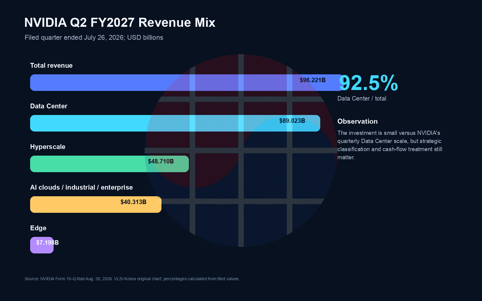
NVIDIA's filed financial baseline changes the scale of the discussion. Its Form 10-Q for the quarter ended July 26, 2026 reports US$96.221 billion of total revenue and US$89.023 billion of Data Center revenue. The filed mix separates US$48.710 billion of hyperscale and US$40.313 billion of AI-cloud, industrial, and enterprise Data Center revenue, with another US$7.198 billion attributed to edge. Consolidated gross margin was 75.0%. Cash, cash equivalents, and marketable debt securities were US$56.586 billion, while marketable equity securities were US$42.8 billion.
That scale means the US$3.5 billion convertible is not a financing necessity for NVIDIA. It is an allocation choice. The same filing reports US$74.421 billion of operating cash flow for the first half and US$42.404 billion of purchases of equity securities. The MediaTek instrument must eventually be classified and measured within that broader strategic-investment activity. The useful next questions are how much cash actually leaves NVIDIA, when conversion can occur, whether the instrument is marked through earnings or another accounting line, and whether additional commercial commitments sit outside the bond.
MediaTek enters from a different baseline. Its monthly revenue page reports NTD349.808 billion for January through July 2026, up 0.84% from NTD346.901 billion in the comparable 2025 period. January through July monthly revenue was NTD46.977 billion, NTD38.954 billion, NTD63.219 billion, NTD46.737 billion, NTD47.434 billion, NTD58.012 billion, and NTD48.475 billion. These are company-wide numbers, not a data-center segment series.
MediaTek's Q1 2026 release supplies the margin and cash context. Revenue was NTD149.2 billion, gross margin 46.3%, operating expenses NTD46.2 billion, and R&D NTD38.345 billion, equal to 25.7% of revenue. Operating income was NTD22.891 billion at a 15.3% margin, and net income was NTD24.376 billion. Cash and current financial assets were NTD194.779 billion. Inventory was NTD85.470 billion, or 87 days, while quarterly operating cash flow was negative NTD17.657 billion.
Those numbers do not prove stress or success in the new program. They show why revenue, gross margin, engineering expense, inventory, and cash must be modeled separately. A custom-XPU program can increase reported revenue while consuming cash for design work, masks, package qualification, inventory, long-lead capacity, and customer support. A convertible can fund that working interval, but it does not remove it.
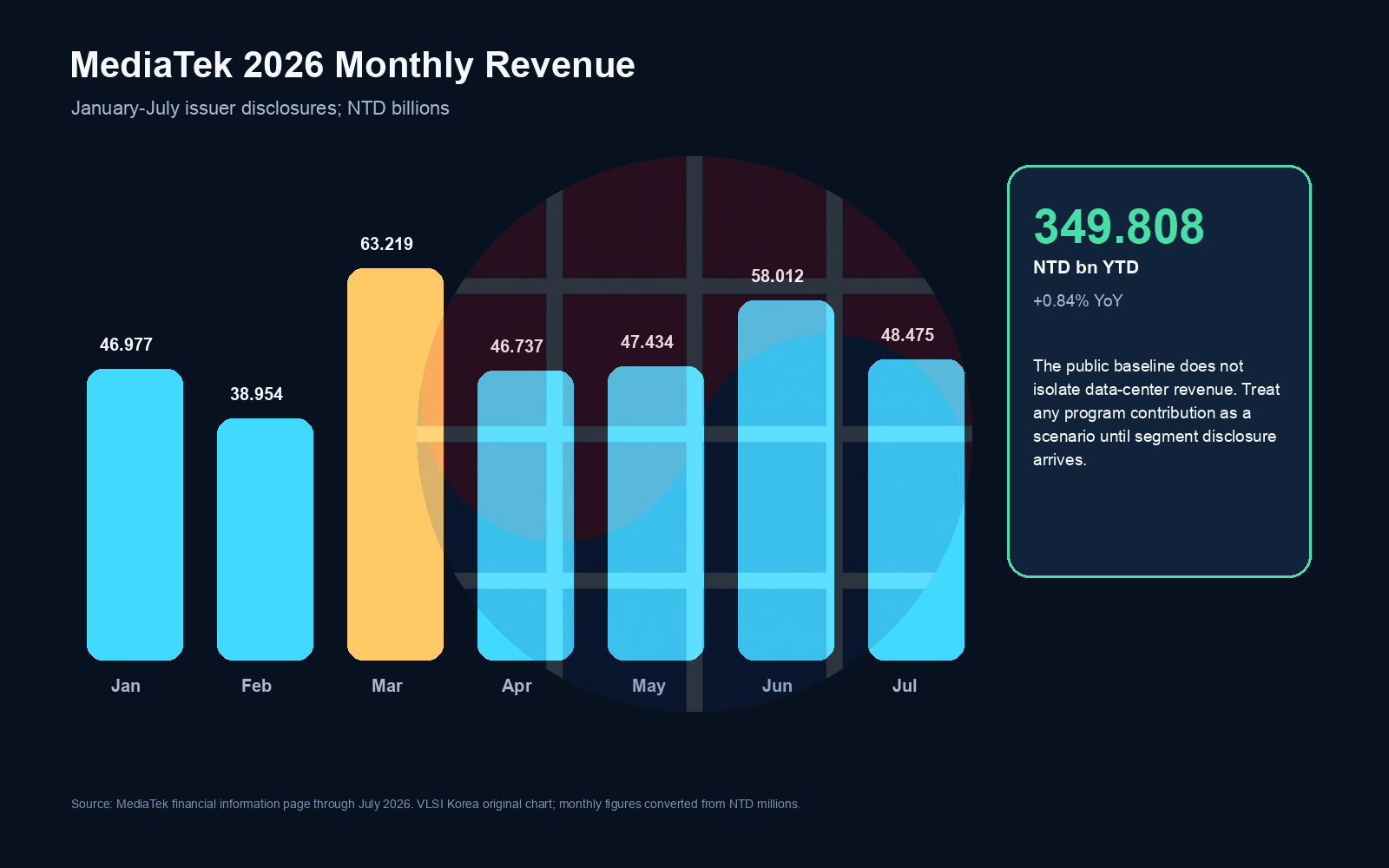
2. The thesis is about attach, not just the compute die
The common description of custom silicon focuses on substitution: a cloud customer replaces part of a merchant accelerator stack with an internally specified XPU. That framing is incomplete. A custom compute die still needs memory, die-to-die links, scale-up connectivity, I/O, packaging, boards, power delivery, cooling, system software, validation, and support. The economic contest is therefore not only who owns the arithmetic logic. It is which interfaces pull the rest of the bill of materials and which party gets paid for qualifying the complete system.
NVIDIA's May 2025 NVLink Fusion release positioned MediaTek, Marvell, Alchip, Astera Labs, Synopsys, and Cadence around a semi-custom ecosystem. It stated a fifth-generation NVLink bandwidth of 1.8 TB/s per GPU, described as fourteen times PCIe 5.0 bandwidth in NVIDIA's comparison. This is an issuer claim for a particular boundary and generation, not a universal system-performance result. It becomes economically useful only when an XPU program actually qualifies that interface and ships at volume.
The August 2026 transaction expands the advertised attachment map. The joint release names prebuilt, prequalified, and system-prevalidated NVLink Fusion elements, a chiplet approach, NVLink-C2C, NVHBM, advanced packaging, SerDes, I/O, and rack integration. Each noun is also a possible profit pool and a possible failure boundary. A prequalified block can shorten development time, but the final customer design still has to reconcile workload, memory capacity and bandwidth, power, thermals, yield, firmware, networking, reliability, and rack operations.
NVIDIA's NVHBM material claims up to 30% more bandwidth per HBM stack than HBM4e, up to a 67% reduction in PHY and supporting-logic area, up to 15% lower HBM power, and up to 30% end-to-end performance improvement per XPU. These are vendor claims under unspecified workload and implementation conditions in the public summary. They should not be entered as realized customer outcomes. The analytical value is that NVIDIA is trying to make memory-interface IP and validation part of the custom-XPU attachment surface, not merely sell a neighboring GPU.
MediaTek's Computex 2026 disclosure describes a complementary full-stack role: custom ASIC and XPU design, 2.5D and 3.5D packaging, high-speed interconnect, rack integration, and co-packaged-optics work. Its cited MicroLED active optical cable power reduction of 50% is also a company claim, not an audited fleet result. Together, the disclosures describe a division of labor in which NVIDIA contributes the fabric, memory interfaces, software ecosystem, and system qualification, while MediaTek contributes customer-specific silicon and integration capability.
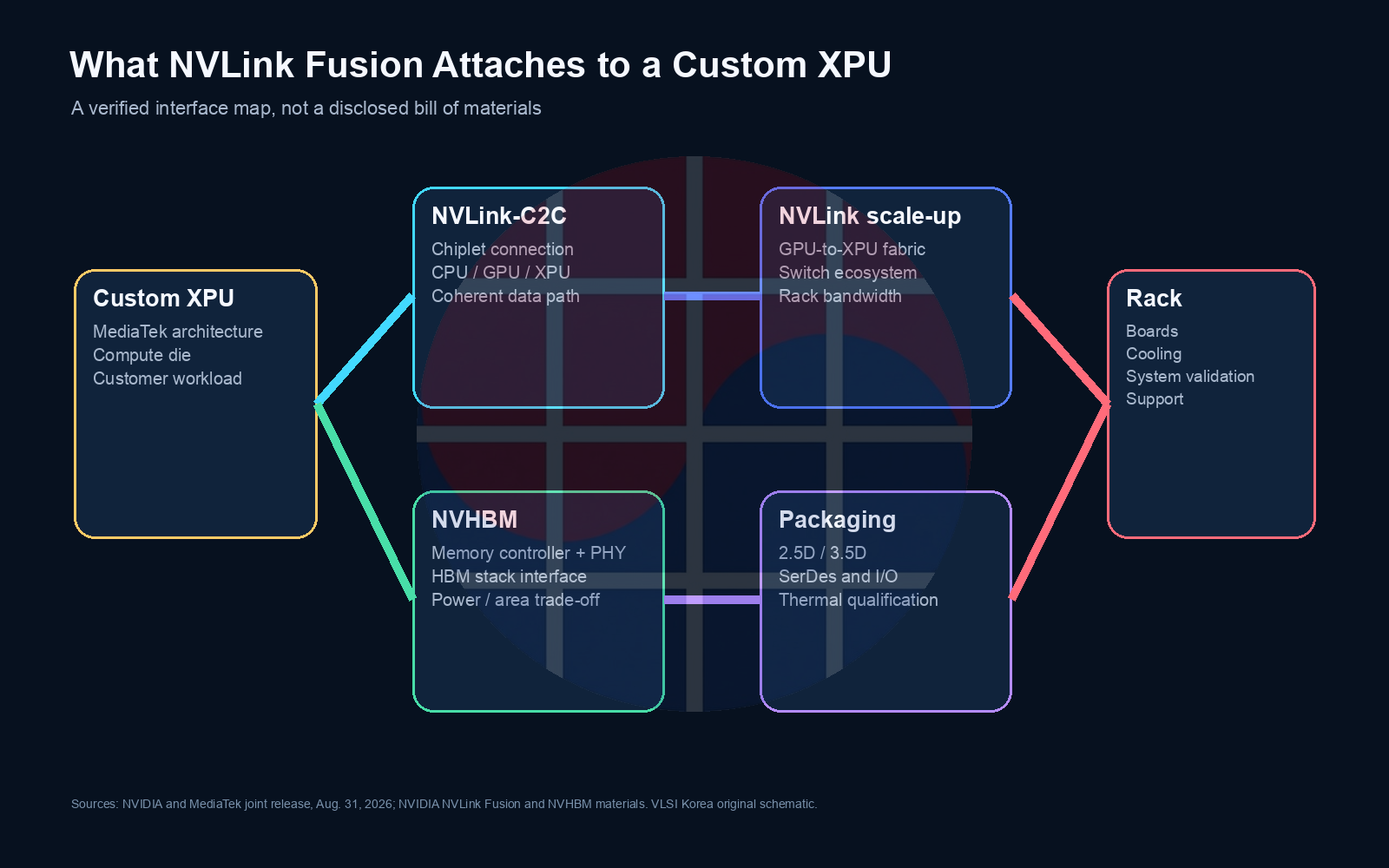
The collaboration has at least one shipped precedent. MediaTek's October 2025 DGX Spark release says the GB10 Superchip was co-designed with NVIDIA and combined a 20-core Arm CPU with an NVIDIA GPU in a system offering up to one petaflop of AI performance and 128 GB of unified memory. The release says the system can work with models of up to 200 billion parameters and paired systems with models up to 405 billion parameters. These remain product claims, but the shipped collaboration is stronger evidence than a partner logo alone. It demonstrates that architectural coordination can reach a commercial system.
A precedent is not a scale proof. DGX Spark does not disclose hyperscale-XPU volumes, segment margins, or the economics of NVLink Fusion attachment. It merely reduces one category of execution risk: NVIDIA and MediaTek have already co-designed a complex compute product. The new thesis still needs customer-specific tapeouts, production qualification, and repeat orders.
3. Financing has six gates before it becomes recurring cash
The strongest skeptical interpretation is circular financing. NVIDIA funds an ecosystem partner, the partner builds products around NVIDIA interfaces, and the resulting activity may be described as demand before an independent customer has paid. Reuters' report explicitly places the transaction in the debate over circular AI financing. Bloomberg, TechCrunch, and Dow Jones Newswires independently confirm the transaction's scale and custom-silicon context. Cross-checking the announcement establishes that the deal is real; it does not answer whether the ultimate customer cash flow is independent.
To avoid that category error, this article uses a six-rung Bond-to-Revenue Evidence Ladder. Rung one is the funded convertible: definitive terms, cash transfer, use of proceeds, accounting, and conversion mechanics. Rung two is a named commercial program: customer, workload, architecture, delivery responsibility, and economic owner. Rung three is tapeout: design freeze, masks, wafers, and a dated production path. Rung four is qualified package: yield, HBM interface, thermals, SerDes, and reliability have cleared. Rung five is accepted rack: networking, software, power, cooling, and customer acceptance align. Rung six is recurring cash: repeated volume shipments are recognized and collected from customers rather than recycled through partner financing.
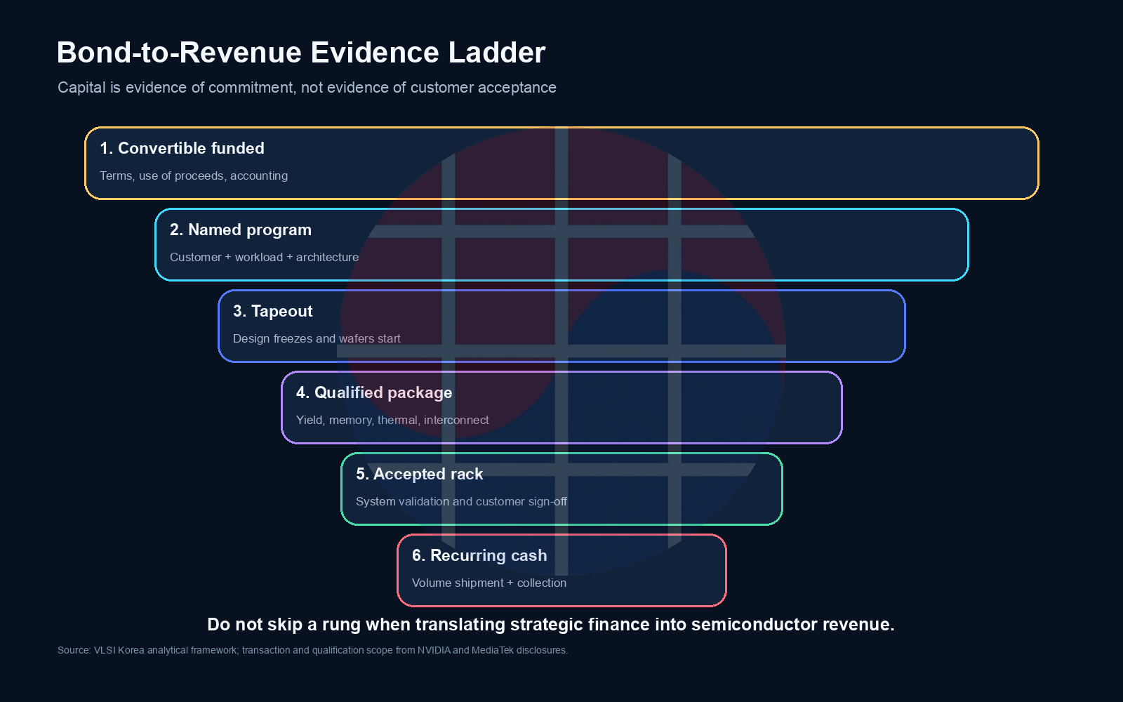
Boundary condition: The US$3.5 billion face amount must not be added to semiconductor revenue, backlog, orders, or data-center total addressable market. It is a financing instrument until contractual and accounting disclosures show otherwise.
The ladder also protects the bullish case from a weak argument. An ecosystem investment can be rational even before customer revenue is disclosed. It may accelerate engineering, reserve packaging or memory capacity, standardize interfaces, secure partner attention, and reduce schedule risk. Those are real strategic options. But they should be described as options and execution capacity, not as completed demand.
Comparable evidence comes from Marvell. Its March 31, 2026 release says NVIDIA invested US$2 billion and that the companies would connect Marvell custom XPUs and scale-up networking with NVIDIA's platform. The recurring pattern is financing plus an attachment stack. The next analytical task is to compare which partner produces named programs, tapeouts, qualified systems, and cash, rather than count investment dollars as market share.
The convertible form introduces separate risks. The bond can preserve MediaTek control while giving NVIDIA upside exposure, but public releases do not yet state the conversion economics. Dilution, coupon, maturity, settlement method, covenants, and strategic rights can change the distribution of value. The same commercial outcome can look different to each company's shareholders depending on those terms. Until filings provide them, any implied ownership percentage or return calculation is speculation.
4. NVLink does not compete with every open interface at the same boundary
A weak comparison puts NVLink, UALink, UCIe, and PCIe in one bandwidth table and declares a winner. The interfaces address overlapping but different system boundaries. NVLink Fusion spans a NVIDIA-centered scale-up and chiplet ecosystem. UALink is an open scale-up fabric. UCIe focuses on die-to-die chiplet connectivity. PCIe remains a general-purpose I/O foundation. Architecture can combine several of them, so adoption at one layer does not automatically eliminate the others.
The UALink Consortium's April 2026 release describes UALink 2.0 support for in-network compute, manageability, and chiplet use in an open scale-up ecosystem. The investment risk for NVLink Fusion is not simply that UALink posts a bandwidth number. It is that silicon, switches, cables, software, compliance, and production systems become interoperable enough that customers can qualify a non-NVIDIA scale-up path without losing schedule or reliability.
The UCIe Consortium's UCIe 3.0 announcement adds 48 and 64 GT/s data rates and manageability features for chiplet interconnection. UCIe may coexist with a higher-level scale-up fabric because a package boundary and a rack boundary are not identical. For MediaTek, a more open die-to-die layer can expand design choice; for NVIDIA, control of the qualified system above that layer can still preserve attachment.
The PCI Express 7.0 specification page states 128 GT/s and up to 512 GB/s of bidirectional bandwidth for a x16 configuration. PCIe's broad compatibility, switching, and I/O role remain valuable. NVIDIA's 1.8 TB/s comparison is intended to show a scale-up performance distinction, but protocol semantics, topology, latency, coherency, software, power, and workload behavior matter alongside raw bandwidth.
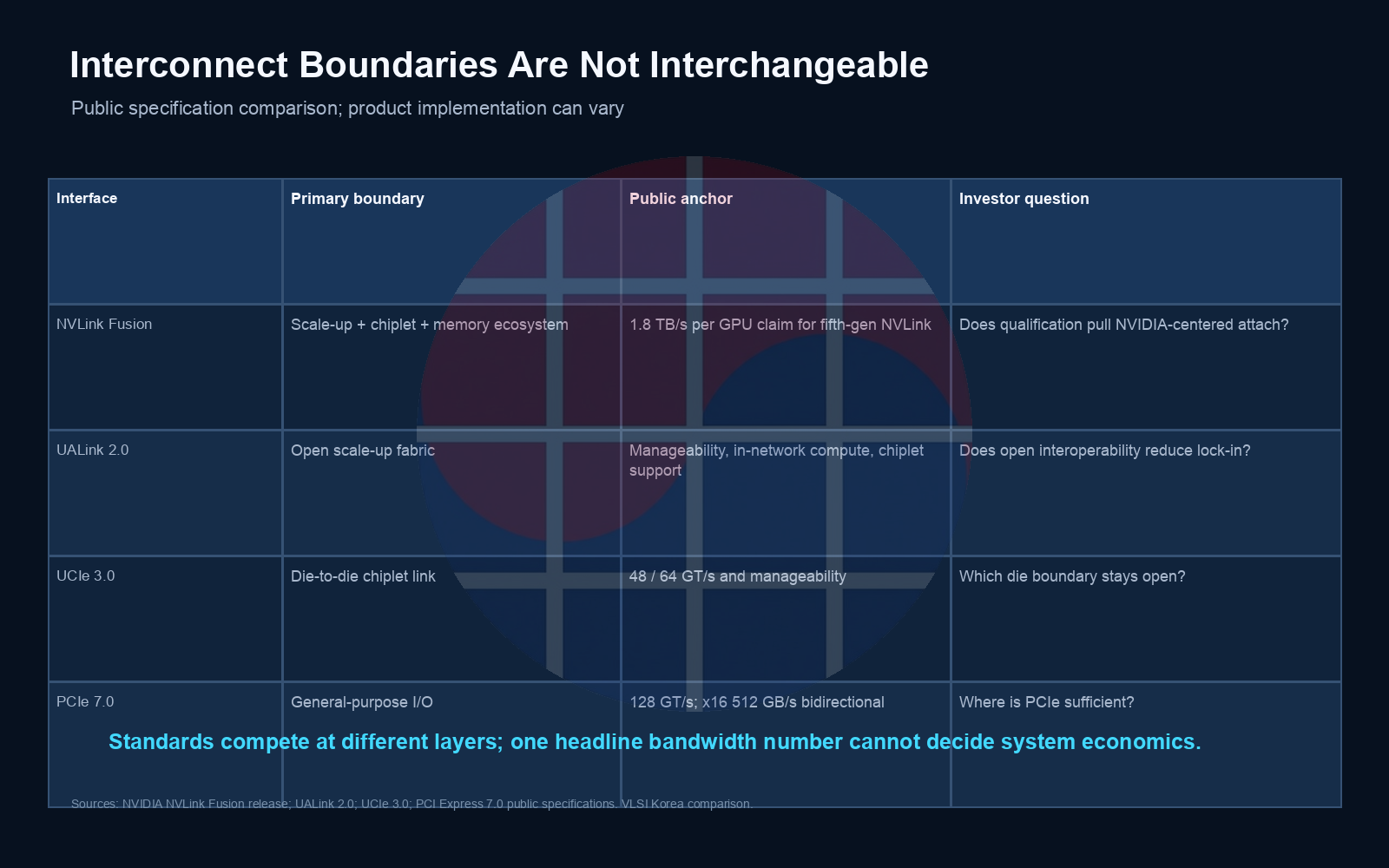
The precise variant perception is therefore not “NVLink wins” or “open standards win.” It is that the profit pool will depend on qualification friction. If NVIDIA and MediaTek provide prevalidated blocks that shorten a customer's schedule, NVLink attachment can earn value even when lower layers are open. If UALink and UCIe ecosystems reach comparable system validation with broader supplier choice, customers can reduce the attachment share. The decisive variables are time-to-qualified-rack, workload performance, reliability, supply assurance, and total cost, not ideology.
This is why the standards checkpoint belongs in the investment thesis. A press release can name a consortium and a specification can be complete while production interoperability remains immature. Evidence should advance through compliant silicon, switches, cable and connector ecosystems, software support, compliance events, reference systems, and independently announced deployments. The same ladder discipline used for the convertible should be applied to open standards.
5. The financial transmission model: volume, price, mix, margin, capex, cash
The economic bridge starts with qualified XPU units, not financed dollars. For a defined period, compute revenue equals qualified units multiplied by realized compute ASP. Attached revenue then adds the products and services that are economically linked to the program: interface IP, chiplets, memory controllers and PHYs, packaging content, SerDes or I/O, switches, optics, boards, rack integration, software, and support. Some of that value may accrue to NVIDIA, some to MediaTek, and much to third-party foundry, HBM, OSAT, substrate, networking, optical, and power suppliers.
Volume depends on named-program count, units per program, yield, customer acceptance, and ramp shape. Price depends on die complexity, packaging, memory interface, service scope, and commercial terms. Mix depends on the fraction of qualified XPUs that use NVLink-connected GPUs, NVHBM, NVIDIA IP, or broader NVIDIA rack components. Margin depends on who bears wafers, HBM, packaging, boards, test, warranty, software, and field support. Capex and working capital depend on masks, tools, inventory, capacity reservations, payment terms, and collection lag.
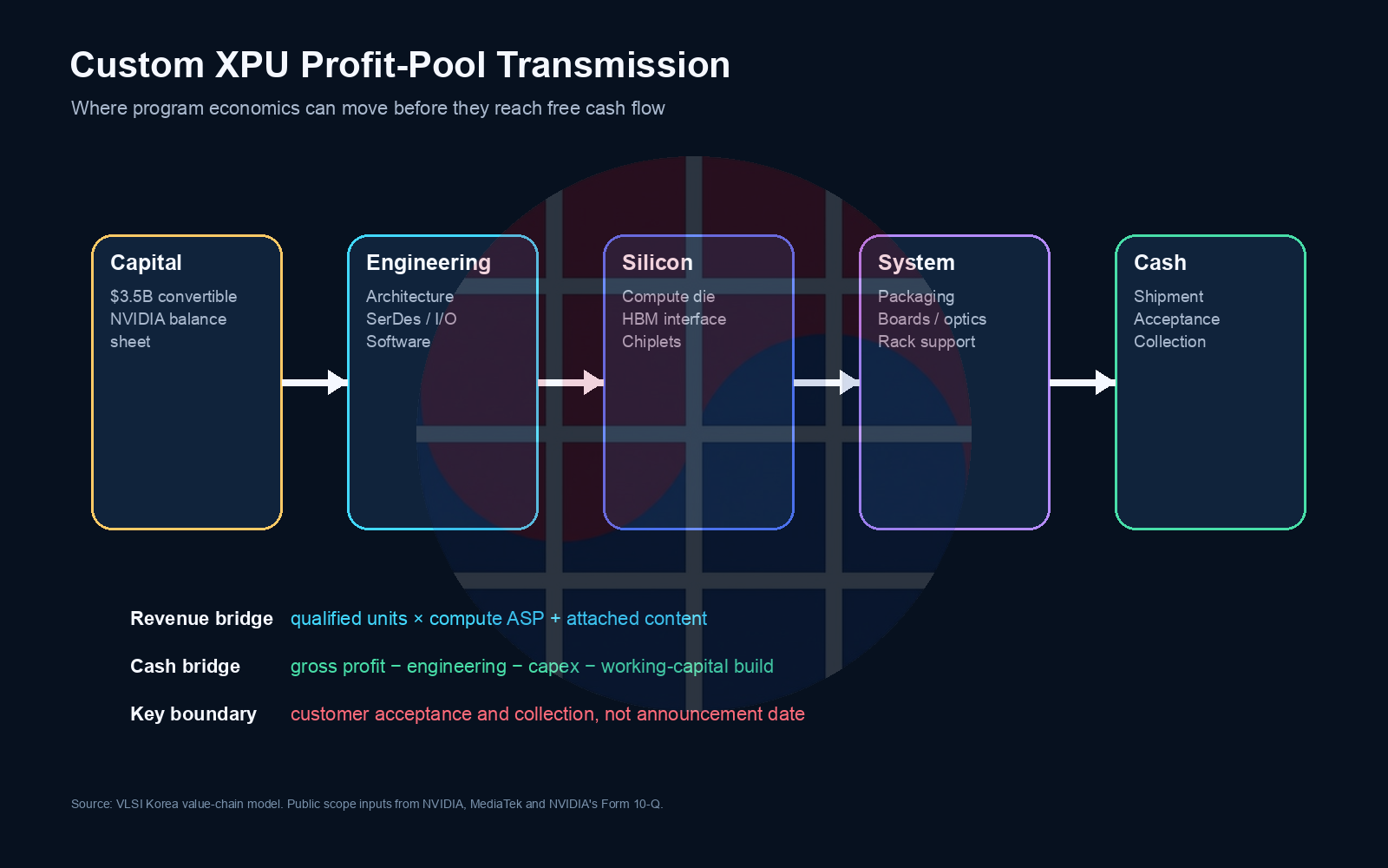
A practical revenue equation is: qualified units × compute ASP × [1 + connected mix × attach-value ratio]. This is a simplification, not accounting guidance. It prevents one common mistake by keeping unit volume, compute price, and attachment separate. A practical cash proxy is gross profit minus incremental engineering, program capex, and working-capital build. It prevents a second mistake by showing that a gross-margin-positive program can still consume cash during qualification and ramp.
NVIDIA's filing identifies wafer fabrication, assembly, testing, packaging, boards, and memory among gross-margin cost components. That list explains why an attach thesis can transmit beyond NVIDIA and MediaTek. A custom XPU that reaches production can pull leading-edge logic wafers, HBM stacks, interposers, advanced package capacity, substrates, SerDes, switches, retimers, optical links, power stages, connectors, and cooling. The allocation of revenue and risk depends on contract ownership. Public releases do not provide that allocation.
MediaTek's Q1 consolidated 46.3% gross margin is useful as a baseline but not as a data-center segment margin. Mobile, connectivity, consumer, edge, and data-center products have different wafers, packaging, support, and pricing. The article's base scenario uses 46.3% only as a transparent anchor. The downside and upside margins are sensitivity assumptions. No claim is made that the custom-XPU program already earns any of them.
Working capital is equally important. MediaTek reported 87 inventory days and negative quarterly operating cash flow in Q1 while continuing a high R&D load. A new program can require inventory and engineering before customer acceptance. The convertible may bridge that interval. The quality of the financing thesis improves when disclosures show which expenditures are incremental, which are reimbursed by a customer, whether volume commitments are non-cancellable, and how soon receivables convert to cash.
6. A reproducible scenario, with assumptions exposed
The scenario uses indices because public releases do not disclose program volume or ASP. Base qualified units are normalized to 100 and base compute ASP to 100. The downside uses a unit index of 50 and ASP index of 90; the upside uses 160 and 105. NVLink-connected mix is assumed at 20%, 40%, and 60%. Attached value as a percentage of compute value is assumed at 10%, 15%, and 20%. Except for the 46.3% base gross-margin anchor, these are analytical assumptions, not company guidance.
The calculation is fully reproducible. Downside revenue index = 50 × 90 / 100 × [1 + 20% × 10%] = 45.9. Base revenue index = 100 × 100 / 100 × [1 + 40% × 15%] = 106.0. Upside revenue index = 160 × 105 / 100 × [1 + 60% × 20%] = 188.16, rounded to 188.2. Apply gross margins of 40.0%, 46.3%, and 50.0% to obtain gross-profit indices of 18.4, 49.1, and 94.1.
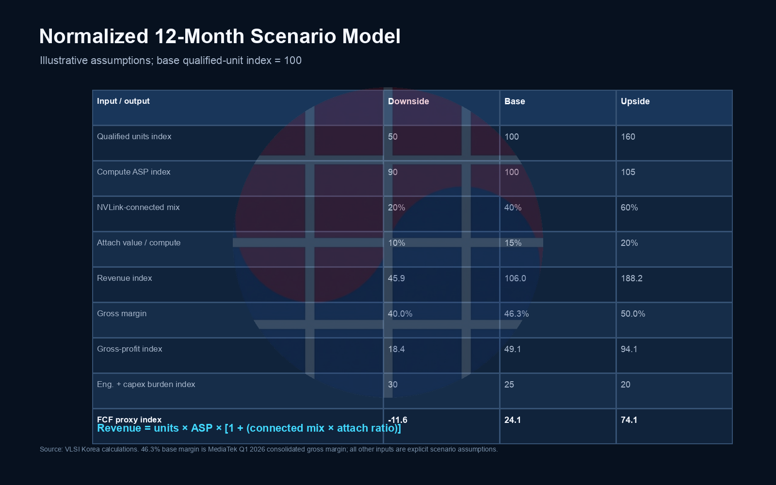
Next subtract an engineering-and-capex burden index of 30, 25, and 20. The resulting free-cash-flow proxy is negative 11.6 in the downside, positive 24.1 in the base, and positive 74.1 in the upside. These values are not forecasts of company free cash flow. They demonstrate a mechanism: low volume and weak attachment can fail to absorb a largely fixed engineering burden, while higher qualified volume and attachment can create operating leverage.
The scenario also assigns illustrative cash-conversion lags of 180, 120, and 90 days. Revenue recognition and collection are not necessarily simultaneous. Package inventory, system acceptance, customer payment terms, and support obligations can widen the interval. A model that reports revenue without an acceptance and collection clock is incomplete for a financing thesis.
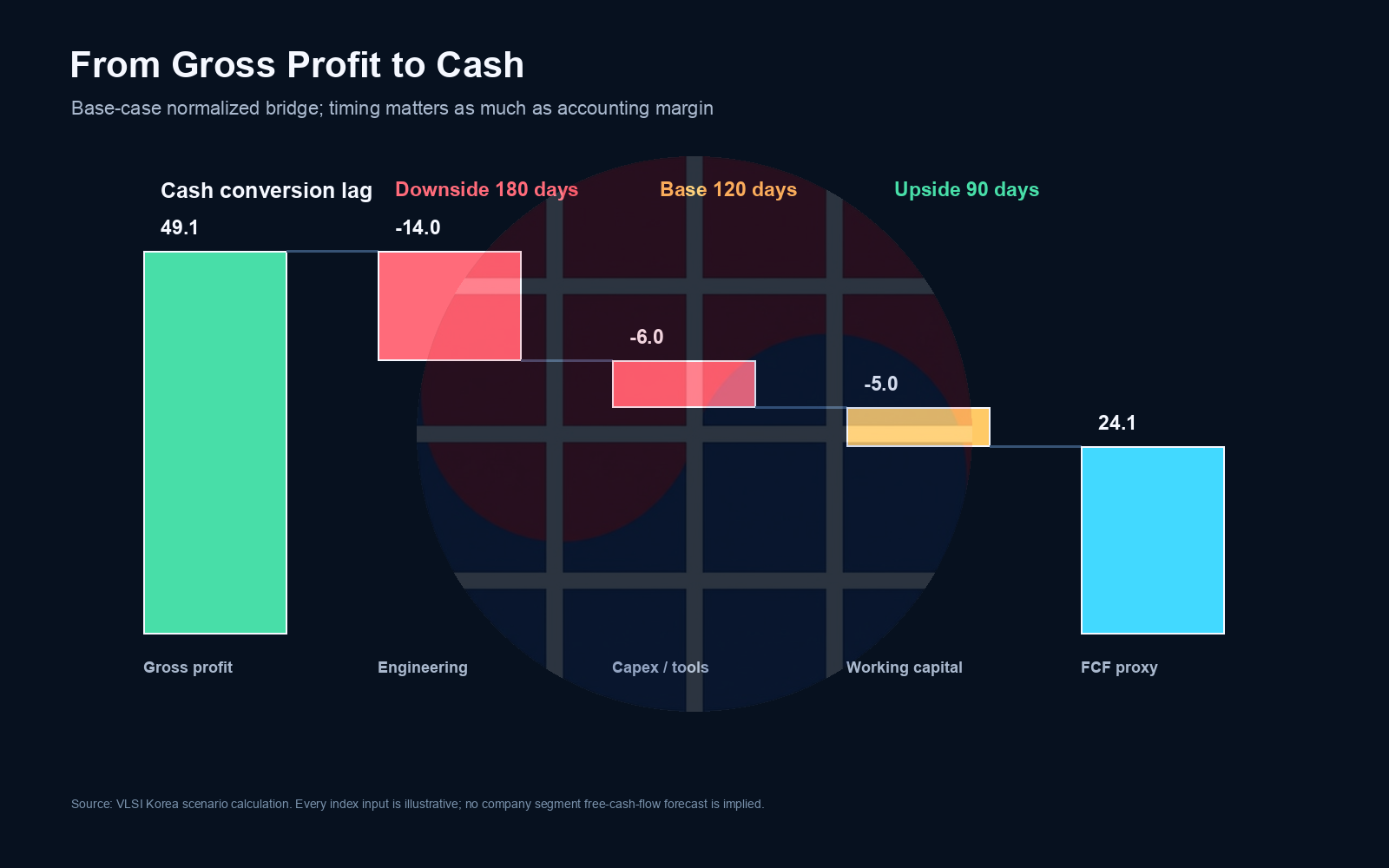
Readers can replace every input as evidence arrives. Named customers and qualified units update volume. Contract disclosures and product mix update ASP and attachment. Segment reporting or management commentary updates gross margin. R&D, mask, packaging, tool, and capacity commitments update the burden. Inventory days, receivables, acceptance, and payment terms update the cash lag. The model becomes more informative by replacing assumptions, not by adding decimals.
A dated falsifier belongs to each case. The downside is too low if multiple named customers disclose qualified production systems, attachment broadens, and MediaTek shows margin and cash conversion without a disproportionate inventory build. The upside is too high if a program slips, open fabrics reduce attached content, support costs rise, or the transaction produces no independent customer cash evidence by the anniversary checkpoint. The base is not a prediction. It is a transparent midpoint whose inputs must move with facts.
Scenario rule: Never mix the US$2 billion company data-center revenue guide with the normalized model as if both were observed custom-XPU revenue. The guide is management's claim for a business category; the model is an analytical sensitivity for one transmission mechanism.
7. Five catalysts, five risks, and the evidence that pairs them
Catalyst one, October 30, 2026: use MediaTek's expected Q3 reporting window to look for definitive bond terms, use of proceeds, named programs, qualification stages, and an updated data-center bridge. The date is a monitoring assumption until the issuer posts its calendar. The paired risk is that general strategic language replaces customer, unit, margin, and cash evidence.
Catalyst two, November 19, 2026: use NVIDIA's expected Q3 filing window to inspect strategic-investment classification, cash-flow treatment, related commitments, and adoption evidence. The paired risk is that the bond sits inside a broader investment program with no separable commercial return or that terms transfer disproportionate risk to one side.
Catalyst three, January 31, 2027: compare MediaTek full-year disclosure with its public data-center narrative. A MediaTek corporate blog published a US$2 billion 2026 AI data-center ASIC revenue guide; an earlier corporate update has circulated with a different timing and scale frame. The correct method is to preserve publication date and scope rather than blend the figures. The paired risk is that no reconcilable segment bridge appears, or that data-center revenue grows while inventory and cash conversion deteriorate.
Catalyst four, April 7, 2027: assess UALink 2.0 one year after its specification release. Look for compliant silicon, switch and cable ecosystems, manageability, software support, reference systems, interoperability results, and production customer use. The paired risk for the NVLink attach thesis is that an open path reaches comparable qualification with broader vendor choice.
Catalyst five, August 31, 2027: at the transaction anniversary, require evidence of named programs, tapeouts, qualified packages, accepted racks, repeat orders, and collected cash. The paired risk is that financing and partnership activity remain visible while independent customer conversion remains absent.
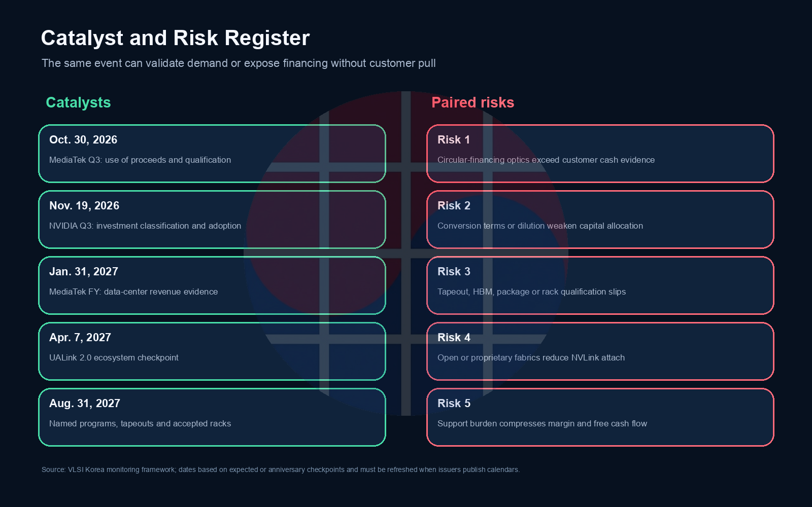
The register is intentionally symmetric. Better disclosure can validate the thesis or expose its weakest link. A high headline revenue number is not automatically bullish if it comes with low margin, high inventory, negative cash conversion, or large support obligations. A delayed program is not automatically fatal if another customer tapes out and the qualification stack becomes reusable. The monitored unit should be the program and its attachment, not sentiment around one press release.
Four explicit thesis breakers matter. First, MediaTek reports no material design-win or revenue conversion at the 2027 checkpoints. Second, UALink production deployments achieve comparable rack qualification and customer breadth without NVLink Fusion. Third, partner gross margin or free cash flow deteriorates because packaging, HBM, and support costs absorb attached revenue. Fourth, independent customer disclosures show that the convertible financed general liquidity without incremental NVLink-connected programs.
8. Korea lens: where the supply-chain evidence should appear
For Samsung Electronics and SK hynix, the relevant demand signal is not the bond amount. It is the number of qualified packages, HBM generation and capacity per package, memory-interface ownership, yield, customer acceptance, and ramp quarter. NVHBM may expand NVIDIA's influence over the memory boundary, but HBM revenue still requires stacks, tested interfaces, qualified packages, and system acceptance. The Korean memory question is whether attachment increases qualified HBM content or merely changes who controls the interface.
For Samsung Foundry and other logic manufacturing teams, custom-XPU value depends on design release, process node, die size, yield learning, wafer starts, and repeat programs. A funded architecture can reserve engineering attention without generating high-volume wafers. Watch mask activity, tapeout statements, advanced-package capacity, and customer ramp evidence. Separate a prototype wafer start from a production volume curve.
For OSAT, substrate, and equipment suppliers, the attachment thesis may be more direct. Chiplets, HBM, 2.5D or 3.5D integration, and high-speed I/O increase package complexity. That can raise content per qualified unit while also increasing yield and schedule risk. The useful metric is not package complexity alone. It is good packages shipped and accepted per unit of constrained capacity, net of rework and test time.
For SerDes, networking, optics, power, board, connector, and cooling suppliers, the rack boundary determines opportunity. A customer can use a MediaTek XPU and still vary the fabric, optical reach, power topology, and cooling design. CPO and active optical cable claims require field validation, reliability data, and system-level energy measurement. An interface win can shift spend across copper, optics, retimers, switches, and connectors rather than simply add to all categories.
For EDA and IP companies, NVIDIA's prequalified-block strategy can increase the value of verified interface IP, models, emulation, SI/PI analysis, thermal analysis, and compliance workflows. It can also narrow merchant opportunity if more blocks are bundled into a platform. Evidence should distinguish tool seats, IP royalties, design-service revenue, and recurring support. A partner announcement is not a disclosed contract for every EDA or IP vendor named in an ecosystem.
For Korean corporate strategy teams, the decision is whether to align capacity and product roadmaps with NVIDIA-centered custom silicon, open alternatives, or both. A portfolio approach can preserve optionality, but qualification resources are finite. The right gate is customer-funded program evidence: named architecture, interface choice, package release, rack acceptance, and volume schedule. Capital allocation should follow those gates rather than a generalized custom-silicon total addressable market.
9. The watch sequence and final judgment
At the announcement date, the observed evidence consists of a US$3.5 billion convertible, a broad collaboration scope, a prior shipped co-design, NVIDIA's strategic investment capacity, MediaTek's revenue and margin baseline, and competing open-interface specifications. The missing evidence consists of bond terms, customer identities, units, ASPs, attachment, segment margins, capex, working capital, and acceptance schedules. The thesis is investable as a monitoring problem only if those two lists remain separate.
By the first reporting windows, expect accounting classification and program-stage language. By full-year reporting, require a reconcilable data-center revenue and cash bridge. By the open-fabric checkpoint, compare system qualification rather than specification headlines. By the transaction anniversary, require independent customers, tapeouts, qualified racks, repeat orders, and cash conversion. If evidence stops at partnership language, the attach thesis has not crossed the ladder.
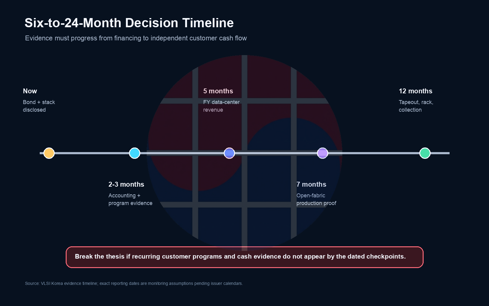
Final judgment: The most defensible current interpretation is neither a completed custom-XPU win nor a meaningless financial loop. It is a financed attempt to make NVIDIA's interfaces the shortest path from customer architecture to qualified rack. The thesis strengthens only when that path produces repeatable, independently funded cash.
The decision checklist has ten items. First, are definitive bond terms filed? Second, is the use of proceeds tied to identifiable programs? Third, are customers and workloads named? Fourth, has a tapeout or production milestone occurred? Fifth, are package, HBM, and fabric qualifications disclosed? Sixth, is the connected mix measurable? Seventh, is segment margin visible or at least bounded? Eighth, are inventory and cash conversion consistent with the ramp? Ninth, do open standards show comparable production qualification? Tenth, do repeat orders and collections come from customers rather than partner financing?
The conclusion is disciplined rather than dramatic. NVIDIA's US$3.5 billion MediaTek convertible can move custom-XPU economics away from a single compute die and toward a qualified attachment stack. The public evidence is sufficient to define the mechanism and monitoring plan. It is not sufficient to claim realized unit volume, attachment revenue, segment margin, free cash flow, or shareholder return. Those are the facts the next six to twenty-four months must supply.
Sources and method
- NVIDIA, joint partnership and convertible announcement, August 31, 2026.
- MediaTek, joint partnership and convertible announcement, August 31, 2026.
- NVIDIA Form 10-Q, quarter ended July 26, 2026.
- MediaTek financial information, monthly revenue through July 2026.
- MediaTek Q1 2026 earnings release.
- NVIDIA NVLink Fusion ecosystem release, May 18, 2025.
- NVIDIA NVHBM technical overview, August 26, 2026.
- MediaTek data-center and rack-integration disclosure, May 28, 2026.
- MediaTek DGX Spark and GB10 co-design release, October 14, 2025.
- MediaTek AI data-center solution and 2026 revenue-guide blog, 2026.
- MediaTek corporate update, publication-date context preserved separately from the later blog.
- Marvell NVLink Fusion partnership release, March 31, 2026.
- UALink Consortium, UALink 2.0 release, April 7, 2026.
- UCIe Consortium, UCIe 3.0 release, August 5, 2025.
- PCI-SIG, PCI Express 7.0 specification page, June 11, 2025.
- Reuters transaction cross-check, August 31, 2026.
- Bloomberg transaction cross-check, August 31, 2026.
- TechCrunch strategy cross-check, August 31, 2026.
- Dow Jones Newswires transaction cross-check, August 31, 2026.
AI assistance note: AI tools supported public-source discovery, arithmetic verification, bilingual consistency checks, visual drafting, and copy editing. VLSI Korea editorial review remains responsible for the thesis, source interpretation, uncertainty labels, and publication decision. Scenario outputs are transparent sensitivities, not company forecasts.
This article is provided for informational purposes only and does not constitute a recommendation to buy or sell any security. Figures and factual statements are based on publicly available sources, including company filings, news reports, and market research, and may contain errors in the source material or in the preparation of this article. The author may own shares in companies mentioned. All investment decisions and their outcomes are the reader's responsibility.
Frequently Asked Questions
What did NVIDIA and MediaTek announce on August 31, 2026?
They announced US$3.5 billion of convertible bonds and work spanning custom XPUs, NVLink Fusion, chiplets, NVLink-C2C, NVHBM, packaging, SerDes, I/O and rack integration. The announcement is not, by itself, evidence that US$3.5 billion of semiconductor demand has already been created.
What terms were not disclosed in the announcement?
The releases did not disclose the coupon, maturity, conversion price or conversion conditions. They also did not disclose named cloud customers, program volume, attach price, segment gross margin, production calendar or collection profile.
What is NVIDIA's financial baseline for the quarter ended July 26, 2026?
NVIDIA reported US$96.221 billion of total revenue and US$89.023 billion of Data Center revenue for the quarter, about 92.5% of the total. Consolidated gross margin was 75.0%, and cash, cash equivalents and marketable debt securities were US$56.586 billion.
What is MediaTek's revenue baseline for 2026?
MediaTek reported NTD349.808 billion of revenue for January through July 2026. That was up 0.84% from NTD346.901 billion in the comparable 2025 period.
Related reading
- Daily Silicon: Only Nvidia Lags as Memory, Arm, and ASICs Power the…
- Daily Silicon: AMD MI355X 250MW, NVIDIA NVLink AI Semiconductors
- Why ByteDance Is Talking to MediaTek: The $80B Custom Silicon Market…
- NVIDIA Vera CPU Deep Dive: Why 1.2 TB/s of Memory Bandwidth Matters…
- NVIDIA's Substrate Bet: 2.5x Capacity, a USD 1.1 Billion Testing…