VLSI Korea
ASIC 역공학의 실제 한계: GDS에서 RTL 의미까지 복원하는 법
ASIC 역공학은 die 사진을 회로도로 바꾸는 일이 아니다. 물리층, gate netlist, sequential state, secret, behavioral validation을 하나의 증거 사슬로 연결하는 방법을 해부했다.


🆓 무료 글 · 누구나 무료로 읽을 수 있는 글입니다
ASIC은 역공학할 수 있다. 다만 무엇을 가지고 무엇까지 복원하려는지가 먼저다. GDS와 PDK, standard-cell library를 가진 foundry-side 분석은 연결성을 거의 결정론적으로 되살릴 수 있다.
패키징된 실물 한 개만 가진 분석은 decap, delayering, imaging, layer registration, device extraction의 오차를 모두 통과해야 한다.
그리고 gate-level netlist는 결승점이 아니다. clock, reset, scan, register, bus, FSM, memory macro를 찾아 architecture와 시간축의 의미를 복원해야 한다. 암호키처럼 제조 후 기록되거나 실행 중 파생되는 상태는 GDS에 없을 수도 있다.
역공학의 난도는 transistor 수보다 evidence gap과 validation depth가 결정한다.
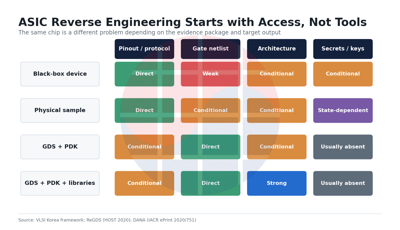
가장 오래 남길 mental model은 이것이다. ASIC 역공학은 사진을 회로도로 바꾸는 작업이 아니라, 서로 다른 증거층을 연결해 검증 가능한 behavioral model을 만드는 작업이다.
이 글은 두 가지 reader job을 겨냥한다. Failure analysis와 security 팀은 어떤 관측 자산으로 어느 수준의 결론까지 방어할 수 있는지 판단할 수 있다. RTL, DFT, SoC architect는 debug와 test 편의가 양산 상태의 attack surface로 남지 않도록 설계 경계를 정할 수 있다.
결정도 두 가지가 달라진다. 역공학 프로젝트를 시작할 때 full-chip imaging부터 살지, 작은 pilot region과 black-box oracle부터 검증할지 선택할 수 있다. 제품 설계 때는 topology, persistent secret, runtime secret, mission behavior를 나눠 control coverage를 배치할 수 있다.
1. 같은 ASIC도 네 가지 다른 문제다
첫 질문은 "복원 가능한가"가 아니다. 성공을 무엇으로 정의하는가가 먼저다. Pinout과 protocol을 알아내는 일, clone 가능한 gate netlist를 얻는 일, architecture를 이해하는 일, key나 privileged state를 읽는 일은 서로 다른 프로젝트다.
Black-box device만 있으면 voltage, timing, I/O sequence, reset behavior, error response를 관찰할 수 있다. Functional oracle는 강하지만 내부 topology는 직접 보여 주지 않는다. 반대로 GDS는 mask에 들어간 geometry를 거의 모두 담지만, pin name과 module name, synthesis intent, 제조 후 기록된 state는 말해 주지 않는다.
GDS와 PDK, technology library를 동시에 가진 공격자는 완전히 다른 출발선에 선다. ReGDS 연구는 이 inside-foundry 조건에서 GDSII와 technology library를 사용해 transistor connectivity를 추출하고, 관계 기반 cell matching으로 gate-level netlist를 복원했다. 연구진은 수백 개에서 수백만 transistor 규모의 실험 회로에서 원 설계를 100% 복원했다고 보고했다.
그 숫자를 실물 칩 일반으로 확대하면 안 된다. 논문의 100%는 정확한 layout와 library가 주어진 평가 환경의 결과다. 패키지 실물에서 손상 없이 모든 layer를 촬영하고, polygon과 via를 정확히 register하며, 알 수 없는 cell library와 memory macro를 추론하는 문제는 포함하지 않는다.
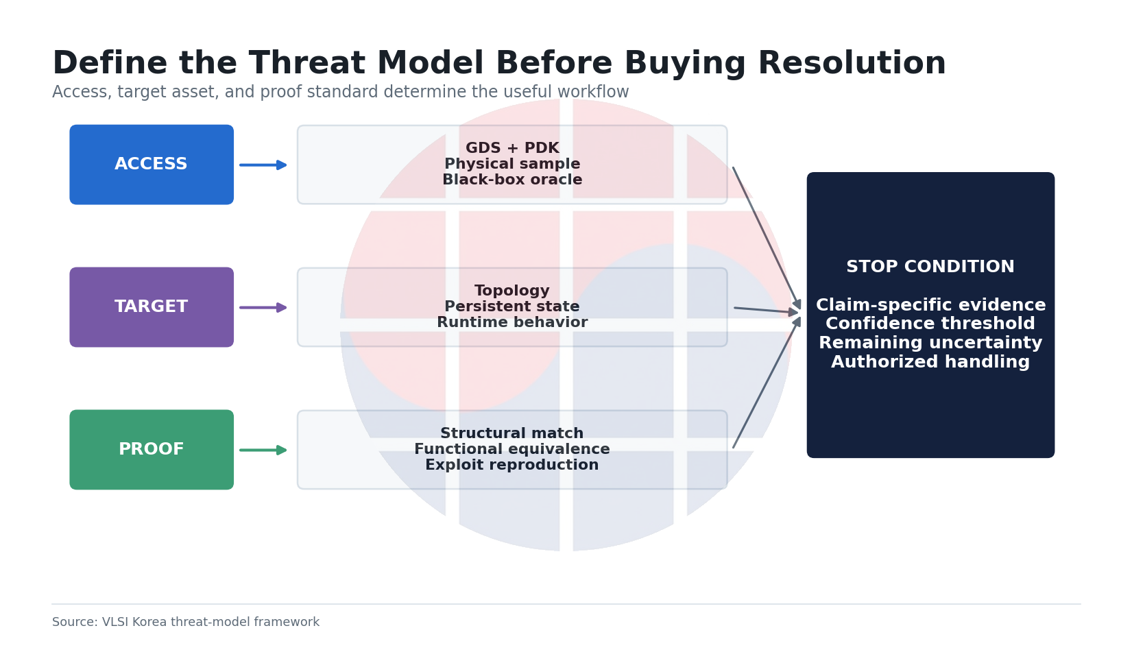
따라서 threat model은 access class를 분리해야 한다. Foundry insider, mask-data 유출, FA lab, returned product, board-level black box, invasive security lab은 같은 "chip access"가 아니다. 각 주체가 가진 golden sample, schematic, test mode, firmware, PDK, library, oracle query 권한을 표로 먼저 고정해야 한다.
2. 실물에서 시작하면 image stack이 첫 번째 회로다
실물 경로는 package identification과 nondestructive observation에서 시작한다. X-ray나 acoustic imaging은 die 수, wire bond, bump, substrate, void 같은 package-level 구조를 보여 줄 수 있지만 transistor netlist를 주지는 않는다. 그 다음 invasive preparation에서 package를 열고 die 접근면을 확보한다.
Frontside 분석은 BEOL metal stack을 위에서 아래로 따라가기 쉽지만 top metal과 passivation, dense fill이 하부를 가린다. Backside 분석은 active region에 가까이 갈 수 있고 local probing이나 fault localization에 유리할 수 있지만 substrate thinning, alignment, device contrast라는 다른 문제가 생긴다.
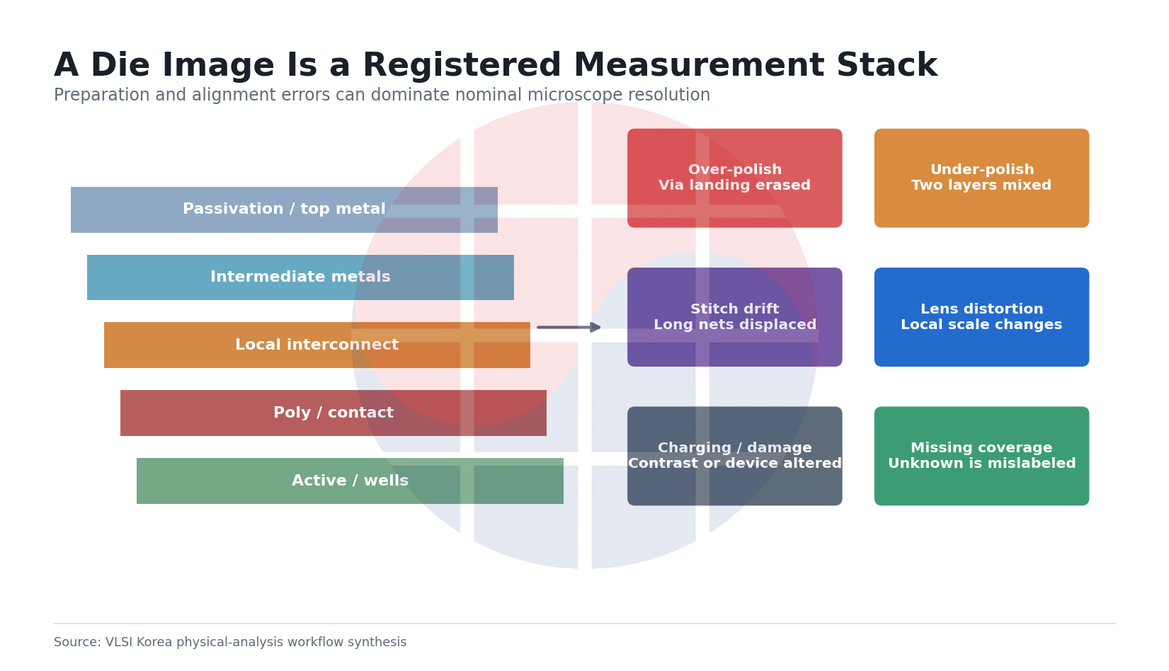
Delayering의 핵심은 한 장의 멋진 사진이 아니다. 같은 좌표계로 정렬된 완전한 layer stack이다. 한 층의 over-polish는 via landing을 지우고, under-polish는 이웃 layer를 섞는다.
Stitching drift와 lens distortion은 멀리 떨어진 net을 잘못 이어 붙인다.
Optical microscopy는 큰 feature와 오래된 node, top-level floorplan에 유용하다. SEM은 더 작은 구조와 material contrast를 제공하지만 field of view, charging, acquisition time, sample damage가 coverage와 충돌한다. FIB는 국소 cross-section과 circuit edit에 강하지만 full-chip mapping을 대신하는 도구는 아니다.
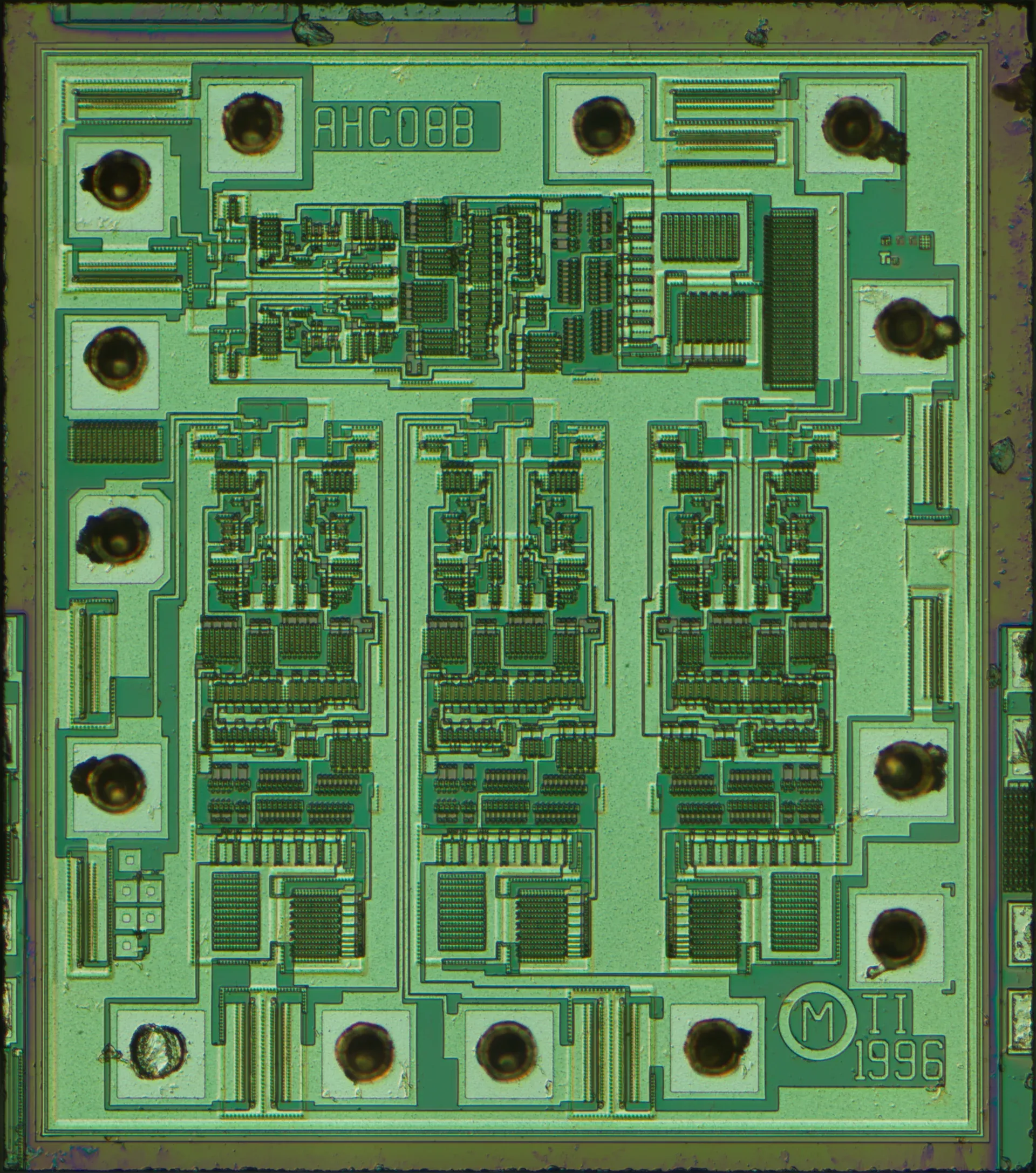
작은 logic IC에서는 repeated gate island, pad ring, protection structure, power rail이 육안 수준에서도 실마리가 된다. 현대 SoC에서는 standard-cell sea, multi-height cell, clock mesh, dense fill, SRAM compiler output, analog macro가 같은 시야에 겹친다. 육안 분류가 가능하다는 사실과 full-chip correctness는 전혀 다른 주장이다.
3. Polygon에서 transistor, cell, net으로
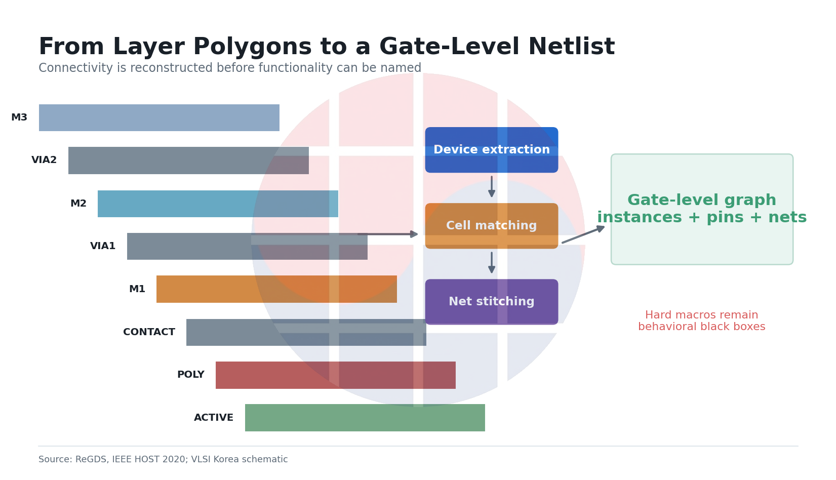
Image stack이나 GDS를 얻은 뒤에는 geometry를 electrical graph로 바꾼다. Active, poly, contact, local interconnect, metal, via를 layer별로 분류하고, overlap과 enclosure rule로 transistor terminal과 conductor connectivity를 만든다.
여기서 extraction의 단위가 중요하다. 가장 낮은 층에서는 MOS device와 resistor, capacitor, diode를 인식한다. 그 위에서는 transistor subgraph를 inverter, NAND, AOI, mux, latch, flip-flop 같은 standard cell instance에 매칭한다.
마지막으로 pin과 routed net을 stitching해 gate-level graph를 만든다.
Library가 있으면 cell boundary, pin geometry, transistor topology를 직접 대조할 수 있다. Library가 없으면 height, rail position, diffusion break, transistor count, Boolean signature로 template를 만들지만 ambiguity가 커진다. Drive strength variant와 threshold-voltage flavor는 logical function이 같아도 physical shape가 다를 수 있다.
Metal fill과 dummy poly는 manufacturability를 위한 geometry지 logic이 아니다. Antenna diode, tie cell, filler, decap, spare cell, ECO route도 function recovery를 교란한다. Extraction system은 "보이는 polygon"과 "전기적으로 의미 있는 object"를 구분해야 한다.
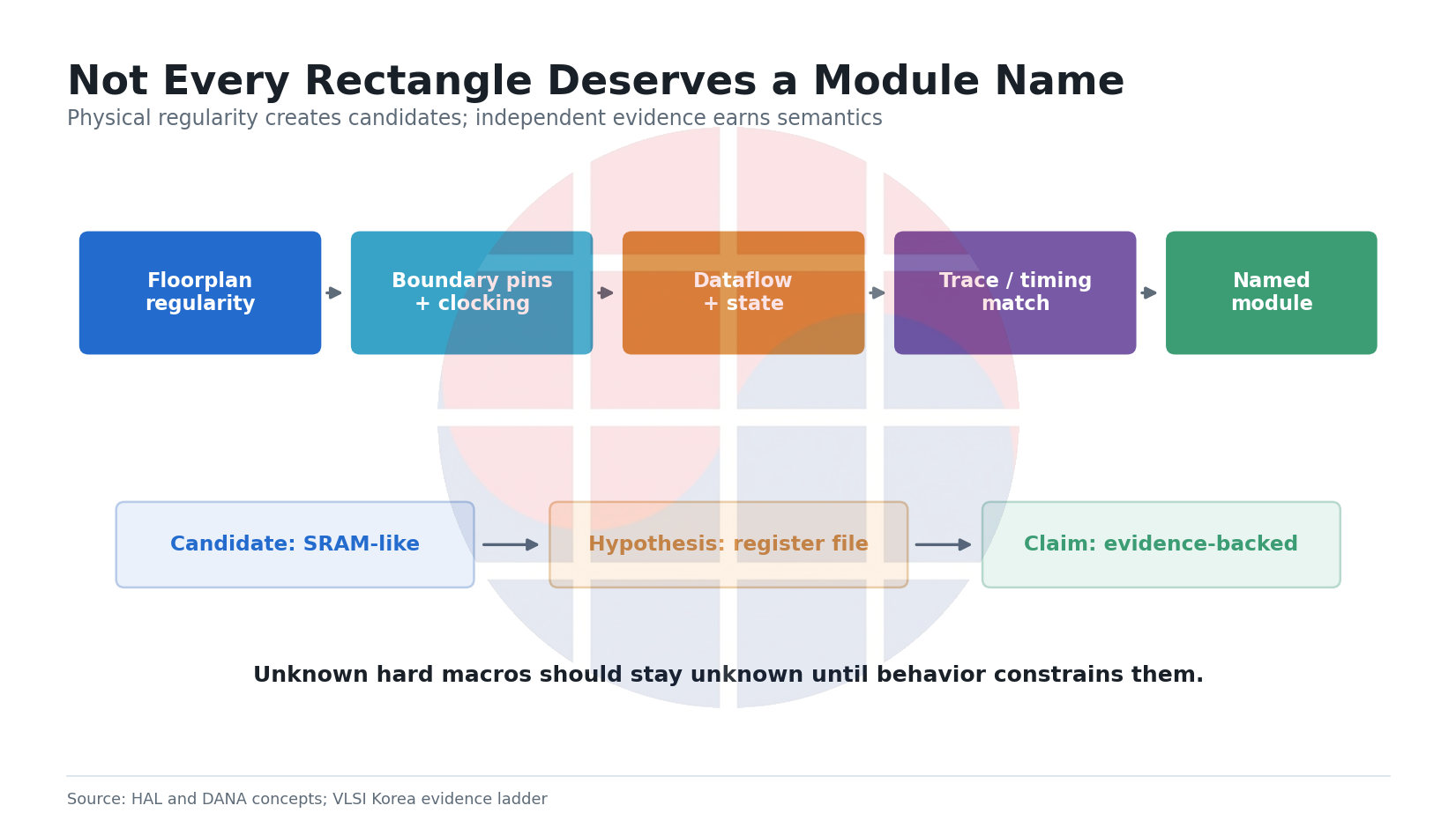
SRAM, ROM, PLL, PHY, ADC, eFuse controller 같은 hard macro는 별도 취급해야 한다. Boundary pin과 access pattern은 보이지만 내부 bitcell이나 analog topology가 standard-cell flow에 맞지 않는다. Macro를 무리하게 flatten하면 정확도보다 false confidence가 먼저 늘어난다.
실무적인 checkpoint는 LVS와 비슷하다. Open, short, floating gate, impossible fanout, power-domain crossing, clock pin misuse를 찾아 graph를 고친다. Golden schematic이 없더라도 local electrical invariants와 cell legality는 강한 self-check가 된다.
4. Netlist가 RTL 의미가 되려면 state를 찾아야 한다
수백만 gate를 얻어도 이름 없는 flattened graph는 사람이 읽기 어렵다. 첫 번째 압축축은 sequential state다. Clock tree와 reset distribution을 찾고 flip-flop을 domain별로 나누면 combinational cone의 경계가 생긴다.
다음은 register와 bus recovery다. 같은 clock, 비슷한 control, 반복되는 fan-in cone, 연속된 bit-slice를 공유하는 FF를 묶는다. Counter는 인접 bit의 carry 관계를, shift register는 규칙적인 predecessor 관계를, register file은 decoder와 mux tree의 반복을 남긴다.
DANA는 flattened gate-level netlist에서 FF 사이 dataflow를 분석해 high-level register를 복원한다. 논문은 crypto co-processor, CPU, OpenTitan을 포함한 9개 design에서 FPGA와 ASIC synthesis에 관계없이 거의 완전한 register recovery를 보고했다. 이것도 평가 설계의 결과지만, topology보다 state grouping이 의미 복원의 핵심이라는 점을 잘 보여 준다.
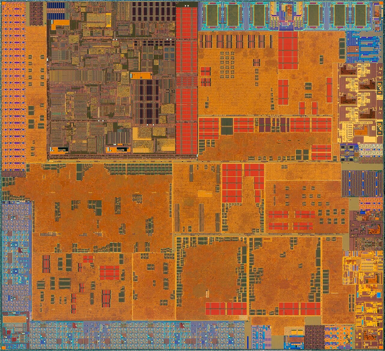
큰 die에서 macro boundary는 density와 regularity로 후보를 만들 수 있다. 그러나 사진의 직사각형을 CPU, cache, DSP로 이름 붙이는 순간 hypothesis가 된다. 물리적 반복성은 function의 증거가 아니라 추가 검증할 주소표다.
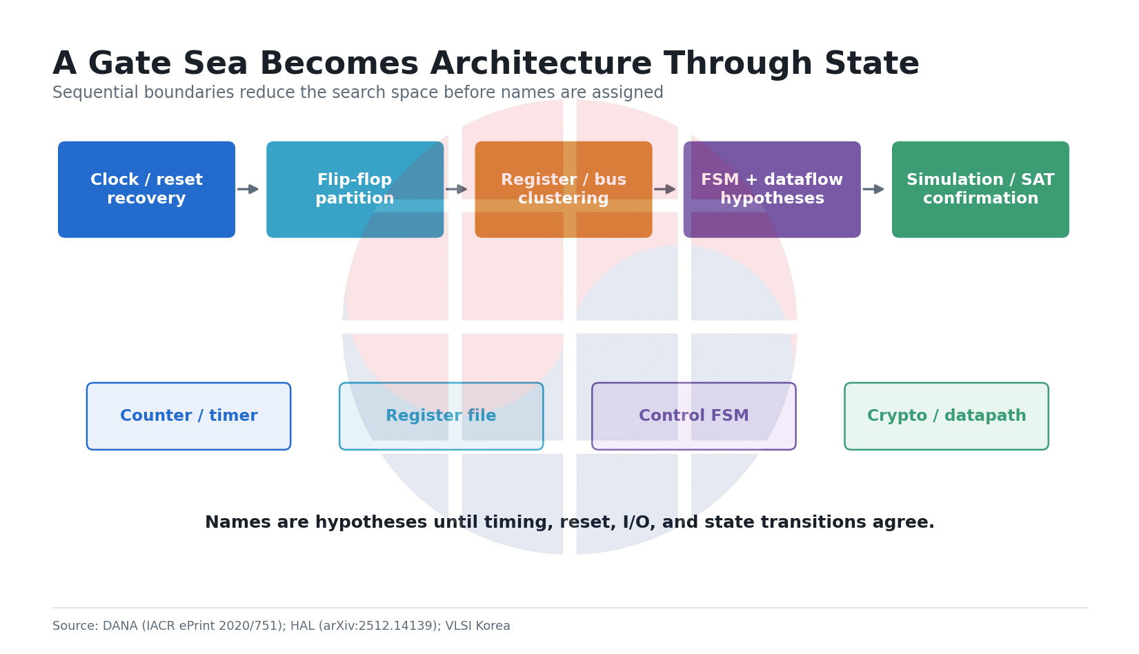
HAL은 이런 분석을 interactive GUI와 C++·Python API, plugin system으로 묶는다. Word-level modularization, graph exploration, simulation, cryptographic analysis plugin을 제공한다. 도구가 module name을 자동으로 "발견"한다기보다 analyst가 hypothesis를 만들고 반복 검증할 수 있는 workbench에 가깝다.
FSM recovery는 state register 후보와 next-state cone을 찾는 데서 시작한다. 하지만 encoded state와 unreachable state, scan mux, synthesis optimization, retiming은 원 RTL의 보기 좋은 case statement를 지운다. 복원 목표는 원문 RTL이 아니라 관측 가능한 behavior와 동등한 state machine이어야 한다.
마지막 단계는 simulation, symbolic execution, SAT/SMT, black-box I/O comparison이다. Reset sequence, legal input constraints, timing protocol을 빼고 combinational equivalence만 보면 sequential chip을 오해하기 쉽다. 일부 output이 맞는다는 사실은 내부 hypothesis 전체가 맞다는 증거가 아니다.
5. Key는 layout이 아니라 state에 있을 수 있다
가장 흔한 오해는 "GDS를 보면 secret도 보인다"는 것이다. Mask ROM content는 geometry에 encode될 수 있다. 하지만 eFuse와 OTP는 cell layout와 programming state가 다르고, flash·EEPROM은 charge state를 읽는 별도 관측이 필요하다.
SRAM과 register의 runtime value는 전원이 꺼진 GDS나 static image에 없다. Secure boot가 root secret에서 session key를 derive하고 export하지 않는 구조라면 최종 key가 영구 저장되지 않을 수 있다. PUF 기반 secret도 physical variation과 evaluation condition의 산물이지 polygon에 적힌 bit string이 아니다.
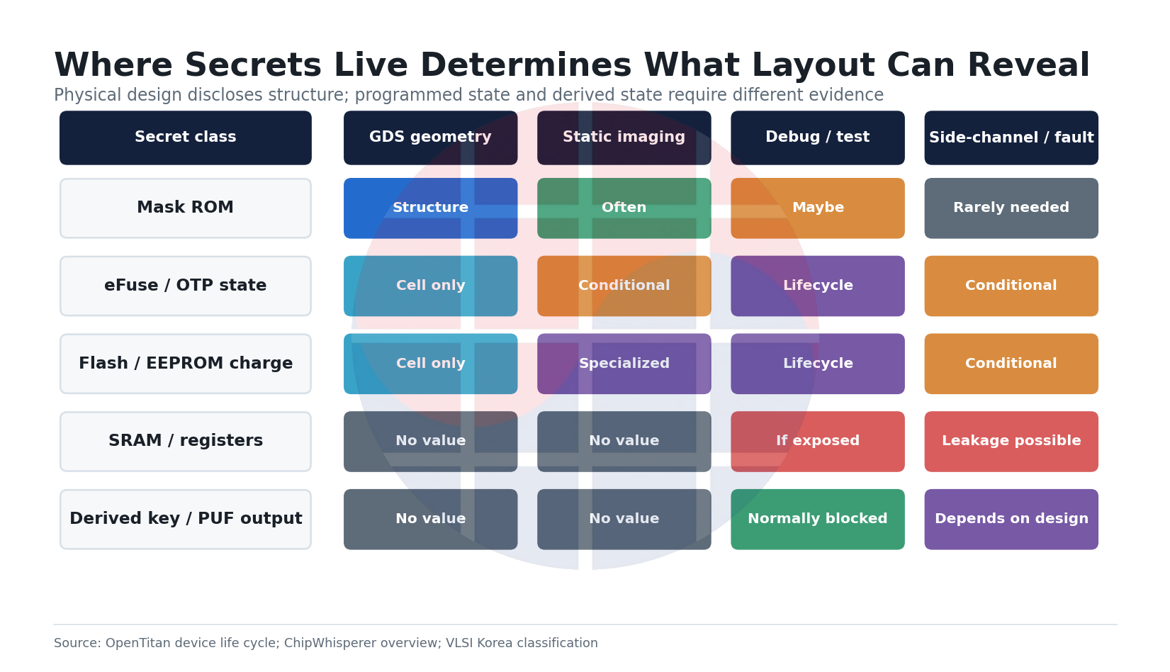
그래서 non-invasive, semi-invasive, invasive 분석은 상호 대체가 아니라 보완관계다. Power와 electromagnetic leakage는 실행 중 data-dependent activity를 관찰한다. Clock나 voltage glitch, electromagnetic 또는 optical fault는 특정 시점의 control flow와 check를 흔들어 hidden state에 대한 oracle를 만들 수 있다.
ChipWhisperer는 power analysis로 consumption leakage를 분석하고 clock·voltage glitch로 unintended behavior를 유도하는 open-source toolchain을 제공한다. 이 사실이 곧 모든 ASIC에 같은 공격이 통한다는 뜻은 아니다. Trigger alignment, noise, countermeasure, package access, clock architecture, detector response가 모두 boundary condition이다.
Debug와 scan은 더 직접적이지만 product life cycle에 묶여야 한다. Manufacturing mode에서 필요한 observability를 PROD까지 남기면 reverse engineer가 비싼 imaging 단계를 건너뛸 수 있다. 반대로 scan을 완전히 없애면 test coverage와 diagnosis, RMA가 무너질 수 있다.
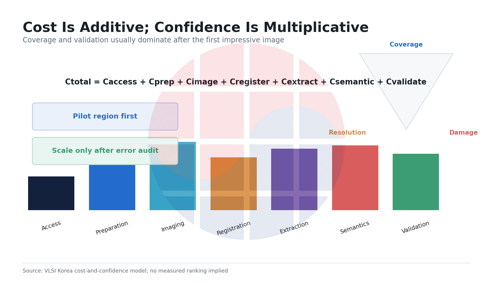
6. 비용은 더하고 신뢰도는 곱한다
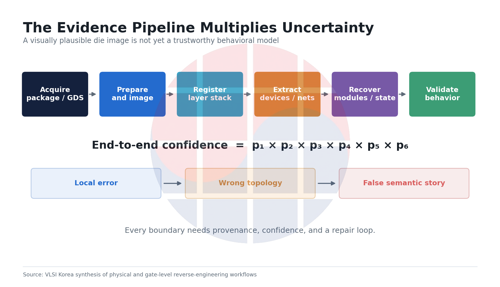
역공학 budget은 대략 access, preparation, imaging, registration, extraction, semantic recovery, validation의 합이다. 그러나 결과 신뢰도는 각 단계 confidence의 곱에 가깝다. 여섯 단계가 모두 99% 정확해도 단순 곱은 약 94%다.
실제로는 error가 독립이 아니어서 한 번의 systematic misregistration이 수천 net을 함께 망칠 수 있다.
Full-chip 최고해상도 imaging부터 시작하는 전략은 비싸고 위험하다. 먼저 pad ring, 작은 standard-cell region, known interface block 같은 pilot area를 선택해 preparation, layer classification, cell matching, connectivity error를 측정해야 한다. 그 뒤에 필요한 resolution과 coverage를 정한다.
Validation에도 level이 있다. Structural validation은 legal cell, pin direction, clock connectivity, power isolation을 본다. Local functional validation은 adder, counter, decoder, CRC, AES round 같은 candidate block의 truth relation을 확인한다.
System validation은 reset부터 I/O protocol, interrupt, DMA, exception, low-power state까지 time-ordered behavior를 비교한다.
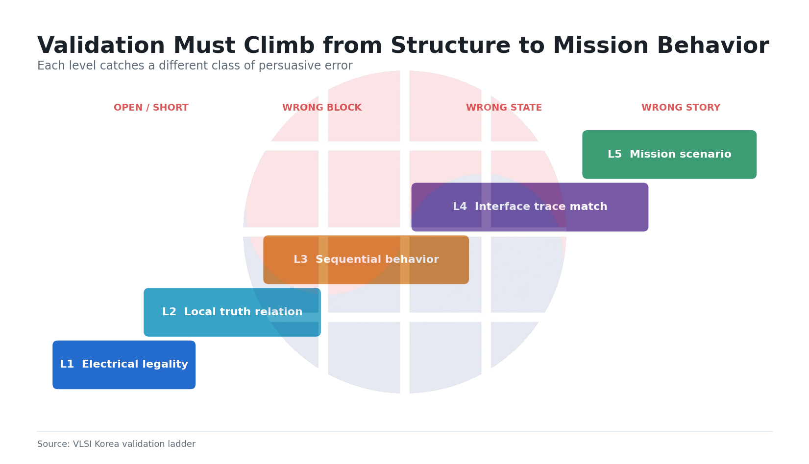
Golden netlist가 없으면 완전한 LEC를 할 수 없다. 대신 여러 독립 invariant를 쌓는다. Physical connectivity, simulation trace, black-box output, timing feasibility, firmware-visible register map이 같은 hypothesis를 지지해야 한다.
맞지 않는 evidence를 nuisance로 버리면 안 된다.
Stop condition도 설계해야 한다. IP litigation은 특정 claim chart에 필요한 block만 충분할 수 있다. Vulnerability analysis는 exploit-relevant path와 security boundary가 목표다.
Clone은 macro behavior, analog performance, process portability까지 요구해 gate netlist보다 훨씬 멀리 간다.
7. 방어는 topology, secret, behavior를 따로 막아야 한다
Layout camouflage와 logic locking은 IP topology 복원 비용을 올릴 수 있다. 그러나 debug가 production에서 열려 있거나 root key가 readable register로 이동하면 topology 방어는 secret 방어가 아니다. 반대로 secure boot만으로 scan leakage나 power leakage를 해결할 수도 없다.
OpenTitan의 device life cycle은 좋은 공개 예다. TEST_UNLOCKED 상태에서는 CPU execution, NVM backdoor, debug, DFT가 활성화된다. PROD에서는 CPU만 활성화되고 NVM backdoor, debug, DFT가 비활성화된다.
RMA는 device-unique token과 owner content erase를 조건으로 invasive observability를 다시 연다.
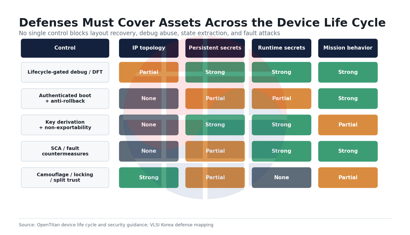
이 architecture에서 중요한 것은 fuse 하나가 아니다. Manufacturing state를 key derivation에 섞고, invasive state로 가기 전에 owner flash를 지우며, OTP secret을 software-readable bus에서 분리한다. Debug 권한과 secret availability가 같은 state에서 동시에 열리지 않도록 설계한다.
DFT sign-off에는 최소 다섯 질문이 필요하다. PROD에서 TAP과 scan instruction이 정말 unreachable한가. MBIST repair data와 eFuse read path가 privilege boundary를 우회하지 않는가.
Test clock과 reset override가 glitch detector를 무력화하지 않는가. RMA unlock이 replay, rollback, shared token에 취약하지 않은가. Debug enable이 synthesis와 physical integration 뒤에도 fail-closed인가.
Crypto block은 constant-time software만으로 끝나지 않는다. Balanced implementation, masking, hiding, randomized execution, sensor와 response, redundant check, fault-resistant control flow의 조합을 threat에 맞춰 선택한다. Countermeasure가 PPA와 testability를 희생하므로 verification plan과 함께 설계해야 한다.
8. Chiplet과 backside power는 경계를 옮긴다
Advanced packaging은 역공학을 단순히 어렵게 만들지 않는다. 어떤 것은 숨기고 어떤 것은 새로 드러낸다. 2.5D interposer와 die-to-die link는 package-level observation point를 늘리고, chiplet별 test와 repair path는 새로운 debug boundary를 만든다.
반면 face-to-face bonding과 hybrid bonding, stacked memory, buried interface는 planar top-down imaging 가정을 깨뜨린다. 한 die를 delayering해도 아래 die와 bond interface의 state를 잃을 수 있다. Backside power delivery는 signal-routing visibility와 probing geometry를 다시 배치한다.
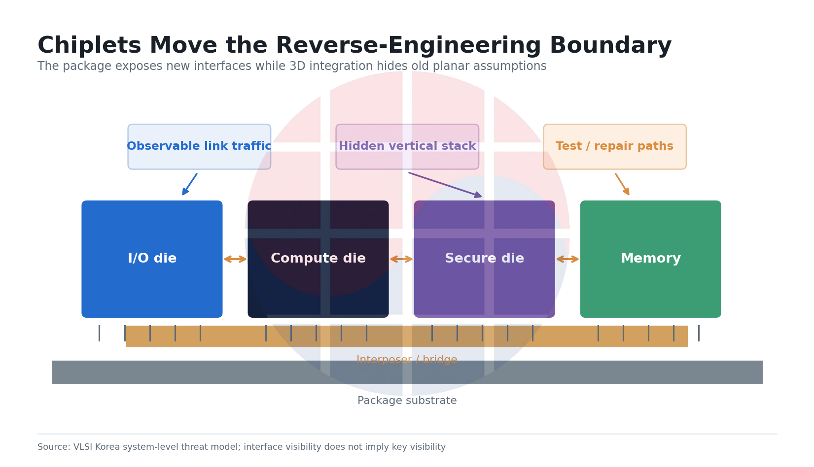
Chiplet security는 "secure die 하나"로 끝나지 않는다. Link training, discovery, firmware update, test access, replay protection, identity binding, key provisioning을 package life cycle 전체에서 닫아야 한다. Untrusted chiplet이 protocol-compliant한 채 traffic pattern과 fault response를 악용할 수도 있다.
한국 생태계에서 이 문제는 fabless만의 일이 아니다. Foundry는 mask와 PDK, library 접근을 통제하고 split manufacturing과 audit trail을 설계한다. OSAT와 advanced packaging 업체는 known-good-die test, interconnect inspection, repair와 RMA 경계를 다룬다.
Memory와 system company는 stack 내부 testability와 customer-visible debug를 분리해야 한다.
대학과 FA lab은 오래된 node의 full-stack reconstruction만 따라가기보다 advanced package cross-section, automated layer registration, netlist semantic analysis, side-channel validation을 연결하는 편이 경쟁력이 높다. 물리분석 장비와 EDA graph analysis가 한 팀 안에서 만나야 한다.
실무 workflow: 먼저 멈출 지점을 설계하라
1. Asset와 adversary를 고정한다. IP topology, firmware protocol, persistent secret, runtime key, safety behavior 중 무엇을 지킬지 적는다.
Adversary의 GDS, PDK, library, physical sample, oracle, lab access를 분리한다.
2. Pilot로 extraction loop를 닫는다. Known block 하나에서 image-to-polygon, polygon-to-device, device-to-cell, cell-to-net error를 측정한다.
Full-chip 예산은 이 결과 뒤에 산정한다.
3. State before semantics 원칙을 쓴다. Clock, reset, scan, power domain, sequential boundary를 먼저 찾는다.
그 뒤 register, bus, FSM, datapath 이름을 붙인다.
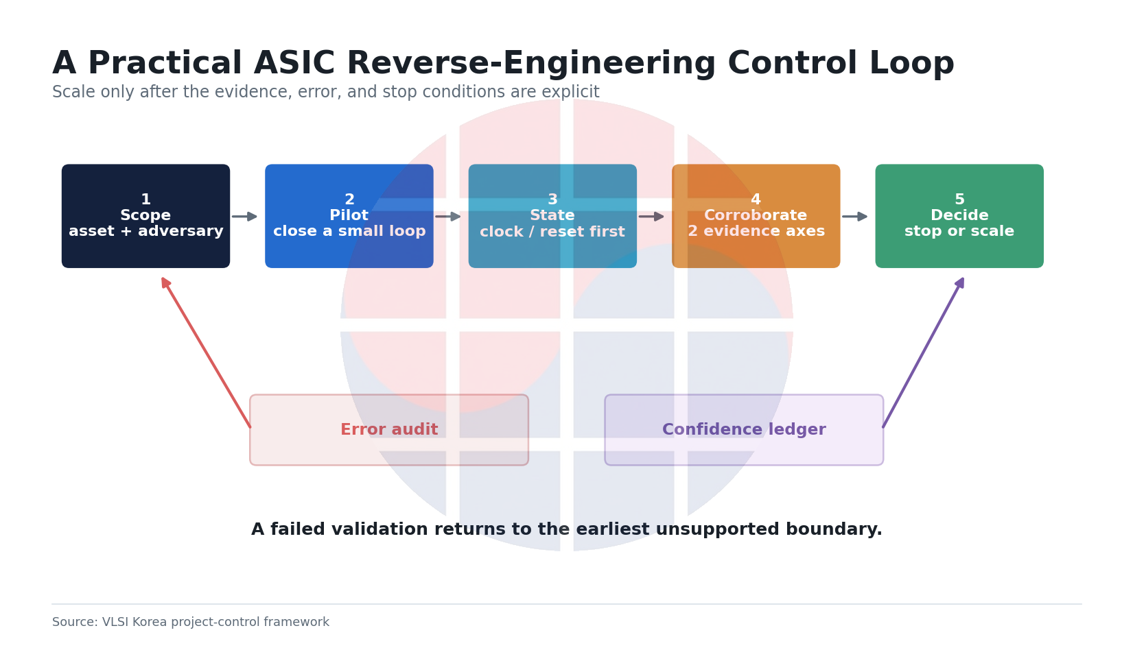
4. 최소 두 개의 독립 evidence로 module을 승인한다. Topology와 simulation, I/O trace와 firmware map, timing과 state transition처럼 서로 다른 축이 같은 결론을 지지해야 한다.
5. Secret storage class를 따로 추적한다. Mask-defined, programmed nonvolatile, volatile, derived, physically unclonable state를 섞지 않는다.
Layout recovery 성공을 key recovery 성공으로 보고하지 않는다.
6. Defense verification을 양산 state에서 반복한다. RTL intent가 아니라 final netlist와 fuse map, boot ROM, test instruction, package pin 상태에서 debug/DFT fail-closed를 확인한다.
FAQ
질문: GDS만 있으면 Verilog를 완전히 되살릴 수 있는가?
답변: Gate-level connectivity는 높은 정확도로 복원할 수 있지만 원 RTL의 module name, parameter, generate structure, comment, microarchitectural intent는 사라져 있다.
복원 결과는 원 source code가 아니라 behaviorally equivalent한 model에 가깝다.
질문: Die shot만 보고 CPU와 cache 위치를 알 수 있는가?
답변: Regularity와 density로 macro 후보를 만들 수는 있다.
정확한 기능명은 connectivity, interface, timing, state behavior로 확인해야 한다.
질문: 최신 node는 역공학이 불가능한가?
답변: 불가능보다 비용 곡선이 급해진다는 표현이 정확하다.
Feature size, layer 수, fill, FinFET·GAA geometry, backside power, 3D integration이 preparation과 imaging, registration cost를 높인다. GDS를 가진 insider에는 이 물리 장벽이 적용되지 않는다.
질문: Logic locking이면 충분한가?
답변: 아니다.
Oracle access, key storage, scan, fault response, structural leakage에 따라 locking이 우회될 수 있다. Asset별 control stack이 필요하다.
질문: Security와 failure analysis는 같은 기술을 쓰는가?
답변: 관측 기술은 많이 겹친다.
다른 점은 authorization, chain of custody, stop condition, disclosure, destructive handling이다. 합법적 FA와 security evaluation은 명시적 권한과 sample disposal 규칙을 가져야 한다.
VLSI Korea view, thesis breaker, 다음 관측점
Consensus: Imaging resolution과 AI cell recognition이 좋아지면 ASIC 역공학은 계속 자동화된다. VLSI Korea view: 가장 큰 병목은 image recognition 하나가 아니라 evidence boundary 사이의 검증이다. Physical extraction, sequential semantics, state acquisition, behavioral validation을 하나의 confidence ledger로 묶는 팀이 우위를 갖는다.
정확한 disagreement는 "AI가 die image에서 RTL을 바로 복원한다"는 기대다. AI는 segmentation, cell classification, graph clustering, module hypothesis를 가속할 수 있다. 그러나 foundry library 부재, hard macro, programmed state, unreachable sequence, false-positive module name을 스스로 ground truth로 만들 수는 없다.
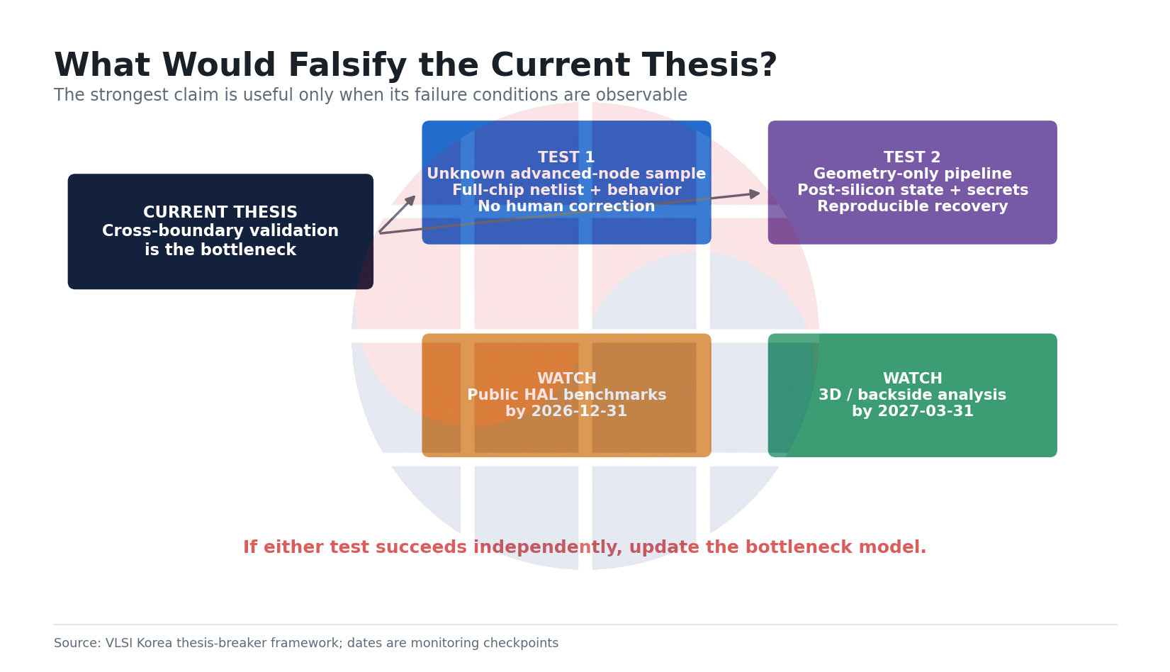
이 thesis를 깨는 사건은 두 가지다. 첫째, unknown advanced-node physical sample에서 full-chip netlist와 system behavior를 human correction 없이 독립 검증한 공개 결과가 나오는 경우다. 둘째, post-silicon state와 secret까지 geometry-only pipeline이 재현성 있게 복원하는 경우다.
다음 관측점은 2026년 12월 31일까지 공개되는 HAL의 word-level·simulation plugin 평가와 새로운 netlist benchmark, 2027년 3월 31일까지 공개되는 backside power 또는 face-to-face stack의 physical analysis 사례, 2027년 6월 30일까지 공개되는 production lifecycle debug와 chiplet security evaluation 방법이다.
관련 VLSI Korea 글로는 Die Shot 분석 ③: 반복 구조가 만드는 성능과 수율, 팀 가이드: Silicon Debug를 함께 읽을 수 있다.
출처
- Rajarathnam et al., ReGDS: A Reverse Engineering Framework from GDSII to Gate-level Netlist, IEEE HOST, 2020.
- Albartus et al., DANA: Universal Dataflow Analysis for Gate-Level Netlist Reverse Engineering, IACR ePrint 2020/751.
- Speith et al., HAL: An Open-Source Framework for Gate-Level Netlist Analysis, 2025.
- Torrance and James, The State-of-the-Art in IC Reverse Engineering, CHES 2009.
- Azriel et al., A Survey of Algorithmic Methods in IC Reverse Engineering, 2021.
- OpenTitan, Device Life Cycle specification.
- NewAE, ChipWhisperer overview.
- Cole L, TI AHC08 die photograph, Wikimedia Commons, CC BY-SA 2.0.
- Cole L, Intel CE3100 die photograph, Wikimedia Commons, CC BY-SA 2.0.
편집 노트: Feature image는 OpenAI image generation으로 만든 개념 이미지이며 실제 die, 제품 또는 측정 결과를 묘사하지 않는다. 본문 도식은 VLSI Korea 자체 작성이다. 외부 die 사진은 각 캡션의 라이선스와 수정 고지를 따른다.