VLSI Korea
Daily Silicon: Samsung, SK hynix: KRW 43.2T HBM, DRAM Facility Spend
A practicing semiconductor engineer's daily read on global silicon news - Samsung, SK hynix: KRW 43.2T HBM, DRAM Facility Spend


🆓 무료 글 · 누구나 무료로 읽을 수 있는 글입니다
A practicing semiconductor engineer's daily read on global silicon news:
Samsung and SK hynix put KRW 43.198 trillion into 1H26 semiconductor facilities, up 35.1% YoY, with memory-line utilization at 100%; HBM capacity, the 2nm design window, QLC NAND density, and the 800VDC power path are resetting lead times together.
Chase's Take - I look at 100% utilization before KRW 43.198 trillion. Backend teams will overestimate shipments if package slots, burn-in, and substrate qualification do not follow higher wafer starts.
The next check is whether 2H26 HBM4 customer qualification moves in lockstep with capacity expansion.
1. Samsung and SK hynix 1H26 Chip Facility Investment Up 35.1%
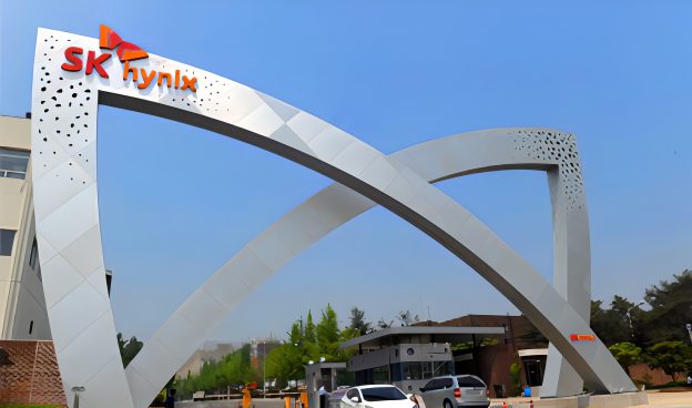
TL;DR - The two companies invested KRW 43.198 trillion in semiconductor facilities in 1H26, up 35.1%, while memory-line utilization reached 100%.
Source: TrendForce - Samsung and SK hynix 1H26 Chip Facility Investment Up 35.1%
2. Samsung Foundry 1.4nm Delayed Three Years to 2029
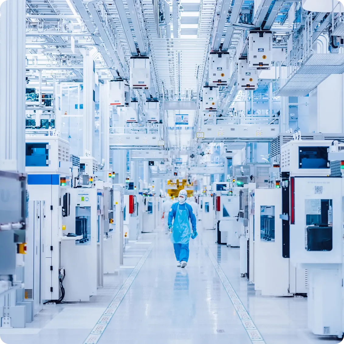
TL;DR - Samsung Foundry moved 1.4nm mass production to 2029, staying on 2nm for three years before preparing High-NA EUV for A10 and below.
Source: Electronics Weekly - Samsung Foundry 1.4nm Delayed Three Years to 2029
3. KIOXIA and SanDisk 10th-Gen QLC: 60% Higher Bit Density

TL;DR - KIOXIA and SanDisk's 10th-generation QLC 3D NAND raises bit density by up to 60% to more than 37 Gb/mm² and reaches a 4.8 Gb/s interface.
Source: EEJournal - KIOXIA and SanDisk 10th-Gen QLC: 60% Higher Bit Density
4. 800VDC: 125kW AI Racks Move to a 1MW Power Path

TL;DR - As AI server racks scale from about 125 kilowatts to 500 kilowatts and then 1 megawatt, 800VDC becomes an architectural shift spanning board power and facility protection.
Source: Semiconductor Engineering - 800VDC: 125kW AI Racks Move to a 1MW Power Path
What to Watch Next
- Samsung and SK hynix 2H26 facilities spend and utilization
This shows how quickly KRW 43.198 trillion of investment converts into wafer starts and actual memory shipments. - Samsung Foundry 2nm PDK and library-qualification schedule
This reveals how the 1.4nm schedule shift changes customer design reuse and tapeout windows. - QLC NAND 4.8 Gb/s interface validation and data-out power
This determines how much of the density gain remains for the AI storage tier's thermal budget and controller design. - 800VDC rack DC protection and thermal signoff
The voltage transition is a system-qualification problem spanning switchgear, busbars, and telemetry, not just converters.
Signal Radar — More Headlines
- Voltage-Droop Control for 2.5D PIM Chiplets (Semiconductor Engineering)
- Rethinking Bond Reliability in High-Density Semiconductor Test (Semiconductor Engineering)
- Space Forge's U.S. Semiconductor-Materials Research Partnership (Electronics Weekly)
- Avnet Silica's Q3 2026 Component Lead-Time Check (Electronics Weekly)
- A Case of DRAM Prices Rising 500% in 12 Months (Tom's Hardware)
- AI Optical-Interconnect Market Outlook for 2030 (Tom's Hardware)
- Power Curtailment Priority for Data Centers Above 50MW (Tom's Hardware)
- Security Challenges in Neuromorphic Embedded Systems (Electronics Weekly)
- Kiwimoore's Hong Kong Listing Plan and AI Interconnect (Electronics Weekly)
- Warning of Renewed GPU Prices and Memory Costs (Tom's Hardware)
- SK hynix on Reasoning-AI Inference Workloads (SK hynix)
Further Reading on VLSI Korea
- VLSI Korea Calendar (2026-08-17): Jobs, Industry Events, and Semiconductor Education
Useful background for the day's semiconductor hiring, industry, and training signals. - What Semiconductor Sales Teams Do: EDA, Equipment, IDM, and Fabless Practice
Useful context on the commercial workflows behind semiconductor supply and design decisions.
Frequently Asked Questions
How much did Samsung and SK hynix invest in 1H26 facilities?
The two companies invested KRW 43.198 trillion in semiconductor facilities in 1H26, up 35.1% year over year. Memory-line utilization reached 100%.
When did Samsung Foundry move 1.4nm production to?
Samsung Foundry moved 1.4nm mass production to 2029, a three-year delay. It will stay on 2nm for three years before preparing High-NA EUV for A10 and below.
What does the 10th-generation QLC NAND achieve?
The 10th-generation QLC raises bit density by up to 60% to more than 37 Gb/mm². It reaches a 4.8 Gb/s interface.
Why do AI racks move to 800VDC?
AI racks scale from about 125 kilowatts to 500 kilowatts and then 1 megawatt. At that scale, 800VDC becomes an architectural shift spanning board power and facility protection.
Related reading
- Daily Silicon: SK hynix CPO and HBM: $97.94B in AI Chip Orders
- Daily Silicon: DRAM Margins Top HBM, Korea April Chip Exports Surge 174%
- Daily Silicon: AMAT WFE Guide to 30%+, Foxconn AI Server Surge, Hynix…
- Daily Silicon: Samsung $1T, KOSPI 7,400, SpaceX Terafab — May 6 Reset…
- Daily Silicon: HBM, ASIC, CPO All Surging — Memory Cycle Extends…