VLSI Korea
400-Layer V-NAND and a 256TB SSD: The Storage Economics of Samsung's NAND Counterattack
Samsung unveiled 400+ layer V-NAND and the world's smallest 256TB SSD. A 58% jump in bit density means structurally lower cost per GB. Offloading KV cache to SSD instead of stacking more HBM is now arithmetic, not story. The storage economics of NAND's rise as AI infrastructure's second margin pool.


30-Second Summary
- Conclusion: At GMIF2026 in Shenzhen on October 15, 2026, Samsung unveiled the industry's first 400+ layer V-NAND (V10) and the world's smallest 256TB enterprise SSD (BM1773). NAND is being redefined from "cheap storage" to "GPU memory extension layer," and the storage tier is emerging as AI infrastructure's second margin pool. (Source: Samsung PRNewswire, 2026-10-15)
- Key numbers: V10 delivers 58% higher bit density, 33% faster I/O, and 25% lower power than V9. The BM1773 spans 16TB–256TB on V9 QLC. The PM1763 is a PCIe Gen6 performance SSD sampling in Q4 2026.
- Why it matters: As AI shifts from training to inference and agentic workloads, KV cache is outgrowing GPU memory. Offloading to SSD instead of stacking more HBM is now an architecture — and it is a cost calculation, not a story.
- Investment read: Watch where the benefits of falling NAND cost-per-GB land — they migrate from SSD makers to data center operators. Enterprise SSDs took 48% of all NAND bits shipped in Q2 2026 and are expected to exceed 50% by year-end.
Background: Three Cards Samsung Played at GMIF2026
On October 15, 2026, the 5th GMIF (Global Memory Innovation Forum) Innovation Summit convened in Shenzhen, China. Co-hosted by the Shenzhen Memory Industry Association and the School of Integrated Circuits at Peking University, it drew more than 3,000 professional attendees. This year's theme: "The Future Built on AI Memory and Storage." (Source)
The keynote speaker was Kevin Yoon, CVP & CTO of Samsung Memory China, with a talk titled "The Memory Revolution: Building the Foundation of Agentic AI." Samsung played three cards that day.
First, the industry's first 400+ layer V-NAND — V10 BV-NAND. Second, a two-track server SSD lineup: the 256TB enterprise SSD BM1773 and the PCIe Gen6 SSD PM1763. Third, zNAND-O, a next-generation NAND architecture for on-device AI. Samsung also received the Outstanding AI Memory & Storage Industry Leadership Award at the summit.
Yoon's core thesis compresses into one sentence: "Once KV cache outgrows GPU memory, an independent shared storage tier becomes inevitable."
As the AI paradigm moves from generative to agentic, multiple agents collaborate on complex tasks and vast numbers of tokens are generated and reused. KV cache capacity and reuse demand have exploded — and KV cache no longer fits inside GPU memory. That is the business context of this announcement.
Business Deep Dive
1. The Economics of 400-Layer Bonding — +58% Bit Density Means Lower Cost per GB
The cost structure of the NAND industry is simple: everything comes down to how many bits you extract from one wafer. More layers mean more bits per wafer area, which means lower cost per GB.
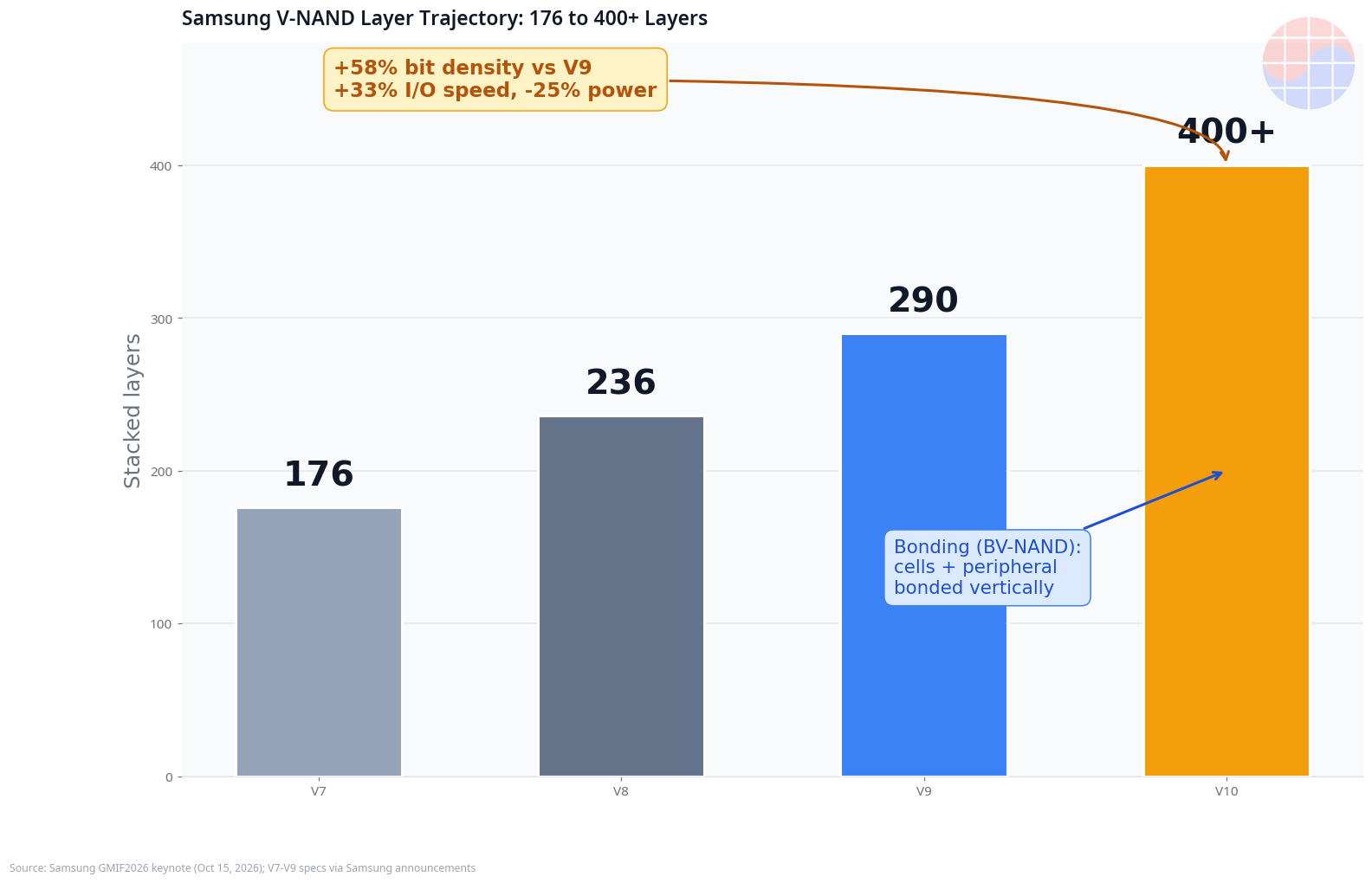
Samsung's V-NAND generation trajectory:
| Generation | Layers | Die Capacity | I/O Interface | Notes |
|---|---|---|---|---|
| V7 | 176 | — | — | Basis of the BM1743 61.44TB QLC SSD |
| V8 | 236 | 1Tb TLC | Toggle 5.0 (2.4 GT/s) | Industry-leading layer count at launch |
| V9 | 290 | 1Tb TLC | Toggle 5.1 (3.2 GT/s) | Double-stack (2×145), 10% lower power |
| V10 (BV-NAND) | 400+ | undisclosed | — | Industry-first 400+ layers; +58% bit density, +33% I/O, −25% power |
(Sources: Pulse/Maeil Business on V9 mass production · KED Global on 290-layer V9 · Samsung PRNewswire, GMIF2026)
The key to V10 is "BV-NAND" — bonding V-NAND. Memory cell arrays and peripheral circuits are manufactured separately, then bonded vertically. Beyond 400 layers, single-stack deposition hits process limits; bonding is becoming the industry-standard workaround.
Through an MBA lens, what matters is not the technology but the economics. +58% bit density means 58% more bits from the same wafer — a structural decline in cost per GB. NAND is a cyclical industry, and cost declines convert into one of two things: (a) lower prices to take share, or (b) held prices to harvest margin. With AI inference demand exploding, Samsung is going for both — premium products like the 256TB SSD to capture margin, and V10's cost advantage to capture volume.
2. The 256TB SSD — What "World's Smallest" Positioning Really Means
The BM1773 spec sheet, as announced:
| PM1763 (Performance) | BM1773 (Capacity) | |
|---|---|---|
| Interface | PCIe Gen6 | undisclosed (enterprise) |
| NAND | V-NAND TLC | V9 QLC |
| Capacity range | undisclosed | 16TB – 256TB |
| Positioning | Performance market | Capacity market — "world's smallest 256TB SSD" |
| Timeline | Sampling Q4 2026 | Announced |
| Target workload | KV cache shared storage | KV cache shared storage |
(Source: Samsung PRNewswire, GMIF2026)
Yoon's line — "With these two SSDs, we will drive both the performance and capacity markets" — is a segment-strategy declaration. The PM1763 takes speed (PCIe Gen6 + TLC + enhanced cooling); the BM1773 takes capacity (V9 QLC).
Consider the business meaning of "world's smallest." In a data center, an SSD's physical size translates directly into capacity density per rack. Fitting 256TB into the same form factor raises storage density per rack and lowers cost per square meter of data center — the TCO metric hyperscalers actually optimize. To a hyperscaler, an SSD is not a component; it is floor space. The BM1773 is aimed precisely at that.
The PM1763's PCIe Gen6 adoption matters too. Gen6 doubles per-lane bandwidth to 64GT/s versus Gen5. In KV cache offload, the bottleneck is the interface, not the NAND cell. Being first with a Gen6 performance SSD is a bid for interface-standard leadership in the AI server generation.
3. The TCO of GPU Memory Offload — A Cost Calculation, Not a Story
The central question of this piece: when GPU memory runs short, why offload to SSD instead of stacking more HBM?
The answer is in the price sheet.
| Memory / Storage | Cost per GB (est.) | Notes |
|---|---|---|
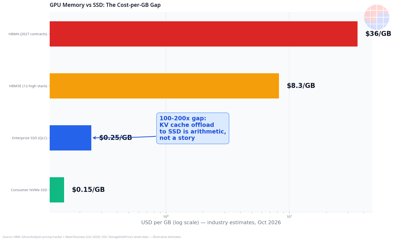
| HBM3E (12-high, 36GB / 288Gb stack) | ~$8.3/GB | ~$300 per stack (industry estimates, Oct 2026) |
| HBM4 (12-high, 36GB / 288Gb stack) | ~$32/GB+ | Samsung negotiating mid-to-high $4 per Gb for 2027 contracts — 3× HBM3E's ~$1.50/Gb |
| Enterprise SSD (high-capacity QLC) | ~$0.15–0.35/GB | 2026 street pricing, supply tight |
| Consumer NVMe SSD | ~$0.11–0.19/GB | Sep 2026 street pricing |
(Sources: SiliconAnalysts HBM pricing tracker · Maeil Business on HBM4 price negotiations · StorageDiskPrices SSD tracker — all industry estimates)
Put HBM4 at ~$32/GB next to an enterprise SSD at ~$0.20/GB and you get a 100–200× per-GB cost gap for the same capacity. KV cache is too big to keep entirely in HBM and too expensive to recompute from scratch. SSDs owning the middle ground is inevitable.
To be clear, SSD bandwidth and latency cannot touch HBM. But KV cache offload is not for "hot" tokens — it is for "warm" context: long-lived shared context across agents, reused system prompts and document chunks. These are not accessed frequently enough to justify HBM residency, yet too costly to recompute every time. A PCIe Gen6 SSD is the economic optimum for that workload.
That is what "a cost calculation, not a story" means. Compare the TCO of adding another HBM stack versus standing up an SSD tier, and the latter wins by orders of magnitude. Samsung's two-track BM1773/PM1763 lineup stands on that arithmetic.
4. zNAND-O — A Wedge Into the Edge-AI Memory Hierarchy
Easily overshadowed by the data center story, zNAND-O may be the most strategic card Samsung played at GMIF2026.
- What it is: A next-generation NAND architecture for on-device AI, now in development in 4-layer and 8-layer versions.
- Structure: Co-packaged next to the MPU, connected via the UCIe interface.
- Specs: 10× the bit density of standard DRAM; 7× the read bandwidth and read energy efficiency of NAND flash.
- Simulation: In a simulation using Moonshot AI's Kimi K2-1T model, an NPU-optimized architecture with zNAND-O cut memory cost to one-quarter at equal performance and fit a nearly 2× larger model.
(Source: Samsung PRNewswire, GMIF2026)
Through an MBA lens, zNAND-O is an attack on the memory hierarchy itself. AI models are expected to exceed one trillion parameters by 2030; keeping all weights in DRAM under the traditional UMA would make on-device costs explode. zNAND-O is not "cheaper DRAM" — it is an attempt to define a new layer next to the processor.
The choice of the UCIe interface is the tell. UCIe is the open chiplet interconnect standard — vendor-neutral. Choosing UCIe over a proprietary bus signals ambition to make zNAND-O an industry-standard layer, not a Samsung-AP-only feature. Whoever defines the layer defines the margin — as HBM demonstrated.
5. Market Structure — Enterprise SSDs Just Ate Half of NAND Demand
The numbers tell the structural story.
| Metric | Figure | Period / Source |
|---|---|---|
| Samsung NAND revenue share | 29.3% (#1) | Q2 2026, industry estimates (BusinessKorea) |
| Samsung NAND revenue share | 29% (#1) | Q1 2026, industry estimates (SamMobile) |
| Global NAND revenue | $46B (3.5× YoY) | Q1 2026 — exceeding all of 2023's revenue (SamMobile) |
| Enterprise SSD share of NAND bits | 48% (vs 26% a year earlier) | Q2 2026; expected to exceed 50% by year-end (Pulse/Maeil Business) |
| YMTC shipment share | 14% (entered global top 3) | Q2 2026, overtaking Kioxia for the first time (Pulse/Maeil Business) |
The structural shift is unambiguous. As AI workloads migrate from training to inference, enterprise SSDs now absorb nearly half of all NAND bits. Consumer supply has tightened and consumer ASPs hit record highs. NAND industry revenue jumped 3.5× in a year.
The competitive landscape is churning too. Samsung, prioritizing higher-margin DRAM, saw its NAND shipment share slip to 25% (shipment basis), while SK hynix rode its Solidigm subsidiary's QLC enterprise SSDs (+40% QoQ bit shipments) to 22%. China's YMTC, mass-producing 267-layer 3D NAND and developing 300+ layer technology, entered the global top three for the first time.
Samsung's GMIF2026 announcements are a counterattack on this battlefield: V10's cost structure + BM1773's capacity leadership + PM1763's performance leadership, aimed at reclaiming the premium enterprise SSD market.
Chase's Take
While HBM grabs the headlines, the real margin migration is happening in the storage tier.
First, NAND is being redefined. For a decade, NAND was "the cheapest storage per GB." Samsung is now repositioning it as "the extension layer for GPU memory that can't hold the KV cache." Category redefinition is margin redefinition — the same bit commands a different price when sold as memory expansion versus sold as storage.
Second, 400-layer bonding is a cost-competitiveness declaration, not a technology race. +58% bit density ultimately means lower cost per GB, and lower cost per GB is pricing power. With YMTC chasing at 300+ layers, Samsung opening the 400-layer era via bonding converts a "layer-count gap" into a "cost gap." In NAND price negotiations, layer count is bargaining power.
Third, zNAND-O is the biggest long-term bet. The BM1773 and PM1763 convert to revenue within 1–2 years, but zNAND-O attempts to change the memory hierarchy itself. Choosing UCIe — an open interface — means building an ecosystem, and whoever builds the ecosystem harvests the standard. It could become the key to on-device cost in the trillion-parameter era of 2030 — with the caveat that it is still in development.
Fourth, the risk is supply. With enterprise SSDs swallowing half of NAND bits, consumer supply has tightened, and Samsung's own DRAM-first strategy constrains its NAND capacity. If V10's cost advantage does not translate into actual shipped volume, the counterattack stays a spec-sheet announcement. PM1763 sampling in Q4 2026 and the V10 production ramp are the verification points.
Implications
For investors - The benefits of falling NAND cost-per-GB migrate from SSD makers to data center operators (hyperscalers). Lower cost per GB cuts the TCO of high-capacity SSDs and expands AI infrastructure storage budgets. The final beneficiary is the buyer of the storage tier. - Enterprise SSD premiumization is structural. In a market where more than half of NAND bits go to servers, consumer NAND faces sustained tight supply and rising ASPs. Watch the margin structures of vendors with high enterprise SSD mix. - The 100×+ gap between HBM pricing (HBM4 negotiated at mid-to-high $4 per Gb) and SSD pricing underwrites the economic logic of KV cache offload architectures. The CXL and PCIe Gen6 memory-expansion ecosystem is worth watching alongside.
For managers - Memory procurement strategy must expand from "securing HBM" to "designing the memory hierarchy." Across the four-tier stack — HBM + CXL + performance SSD + capacity SSD — workload-optimal placement on TCO grounds becomes infrastructure competitiveness. - If you build edge-AI products, track the emergence of UCIe-based memory layers like zNAND-O. The point where on-device model economics change becomes the inflection of your product roadmap. - In NAND vendor selection, the "layer roadmap" is the "cost roadmap." The ramp speed of the 400-layer bonding generation will decide 2027–2028 NAND pricing power.
FAQ
Q1. Why does 400-layer stacking in V10 V-NAND matter?
NAND cost is determined by bits per wafer. With 400+ layers delivering 58% higher bit density than the previous generation, the same wafer yields 58% more bits — a structural decline in cost per GB. That is the source of pricing power and margin. Samsung achieved it with bonding (BV-NAND): manufacturing cells and peripheral circuits separately, then bonding them vertically. (Source)
Q2. Who buys a 256TB SSD (BM1773), and why?
AI data centers (hyperscalers). In the agentic AI era, KV cache has outgrown GPU memory, making an independent shared storage tier inevitable. The BM1773 is a V9 QLC-based capacity lineup spanning 16TB–256TB, billed as the "world's smallest 256TB SSD." Smaller physical size means higher per-rack capacity density and lower data center TCO. (Source)
Q3. What is the difference between the PM1763 and the BM1773?
The PM1763 is the performance flagship with a PCIe Gen6 interface (V-NAND TLC, enhanced cooling, sampling Q4 2026); the BM1773 is the capacity flagship on V9 QLC (16TB–256TB). Samsung declared a two-track strategy to "drive both the performance and capacity markets." Both target KV cache shared storage. (Source)
Q4. How is zNAND-O different from a conventional SSD?
zNAND-O is not an SSD — it is a NAND architecture for a memory layer co-packaged next to the processor (MPU). Connected via the UCIe interface, it delivers 10× the bit density of standard DRAM and 7× the read bandwidth and read energy efficiency of NAND flash. Aimed at on-device (edge) AI, it targets the on-device memory cost problem of the trillion-parameter era around 2030. 4-layer and 8-layer versions are currently in development. (Source)
This article is analysis based on public press releases and industry estimates, not investment advice. Figures reflect announcements as of October 2026 and are subject to market conditions.