VLSI Korea
Samsung's Silicon Photonics Gambit: Who Gets to Define the Optical I/O Layer
A senior Samsung official said the company is considering silicon photonics acquisitions, targeting photonic IC manufacturing from next year to challenge TSMC's COUPE. The next AI chip bottleneck is not compute but chip-to-chip I/O — and the war over who owns the optical I/O layer has begun.


🆓 Free article · Anyone can read this article for free
30-Second Summary
- A senior Samsung official said the company is considering acquisitions of silicon photonics companies (October 2026, via MTN). The plan: start manufacturing photonic ICs next year on 300mm wafers, combining foundry processes, memory, and advanced packaging to challenge TSMC's COUPE platform. Source
- The next AI chip bottleneck is not compute — it is chip-to-chip I/O. Whoever defines the optical I/O layer will capture the next decade of AI chip margins.
- TSMC already defines the architecture through COUPE. NVIDIA's Quantum-X/Spectrum-X photonic switches and Broadcom's Tomahawk 6 switches all run on it.
- The CPO market is estimated to grow from USD 46M in 2024 to USD 8.1B in 2030 (137% CAGR), exceeding USD 20B by 2036.
- M&A is already hot: Marvell paid up to USD 5.5B for Celestial AI; Credo paid USD 750M for DustPhotonics.
- The key read: TSMC defines the architecture; Samsung is trying to buy time through M&A. The value of Samsung's 2029 turnkey CPO is not share — it is dual-source optionality.
Background: Why Light, Why Now
Copper inside the data center hit its physical wall in 2026. Each GPU needs 800 Gb/s of outbound bandwidth — soon 1.6 Tb/s. Today's pluggable optics draw 12–15W per port; for a 100,000-GPU cluster, pluggable optics alone consume 10–15 MW, or 10–15% of the entire data-center power budget. Copper interconnect loses signal integrity above 200 Gbps per lane.
The answer is CPO (Co-Packaged Optics): placing the optical engine inside the same package as the switch or GPU ASIC instead of routing signals over copper to a faceplate module. CPO cuts 800G port power from 15W to 5.4W (−65%) and total network power by 3.5x. It is the only realistic answer to the 2026–2027 AI cluster constraint.
Against this backdrop, a senior Samsung Electronics official told MTN in October 2026 that Samsung is considering acquisitions involving silicon photonics companies. The plan is specific: enter the photonic IC market next year using 300mm wafer processes, targeting optical-module makers such as Coherent and Lumentum as customers, along with fabless companies that design photonic ICs. Start by selling wafers; expand into combining electrical ICs with photonic ICs and optical packaging. Source
What matters here is not the entry announcement but the admission of lateness. MTN reports TSMC's roadmap is roughly one to two years ahead of Samsung's. Samsung is currently validating its optical technology with an "alpha customer."
Business Deep Dive
Market Size: From USD 46M to USD 8.1B
The CPO growth curve is among the steepest in semiconductor history.
| Year | CPO Market Size (est.) | Note |
|---|---|---|
| 2024 | USD 46M | Lab and pilot stage |
| 2030 | USD 8.1B | 137% CAGR |
| 2036 | USD 20B+ | 37% CAGR, 2026–2036 |
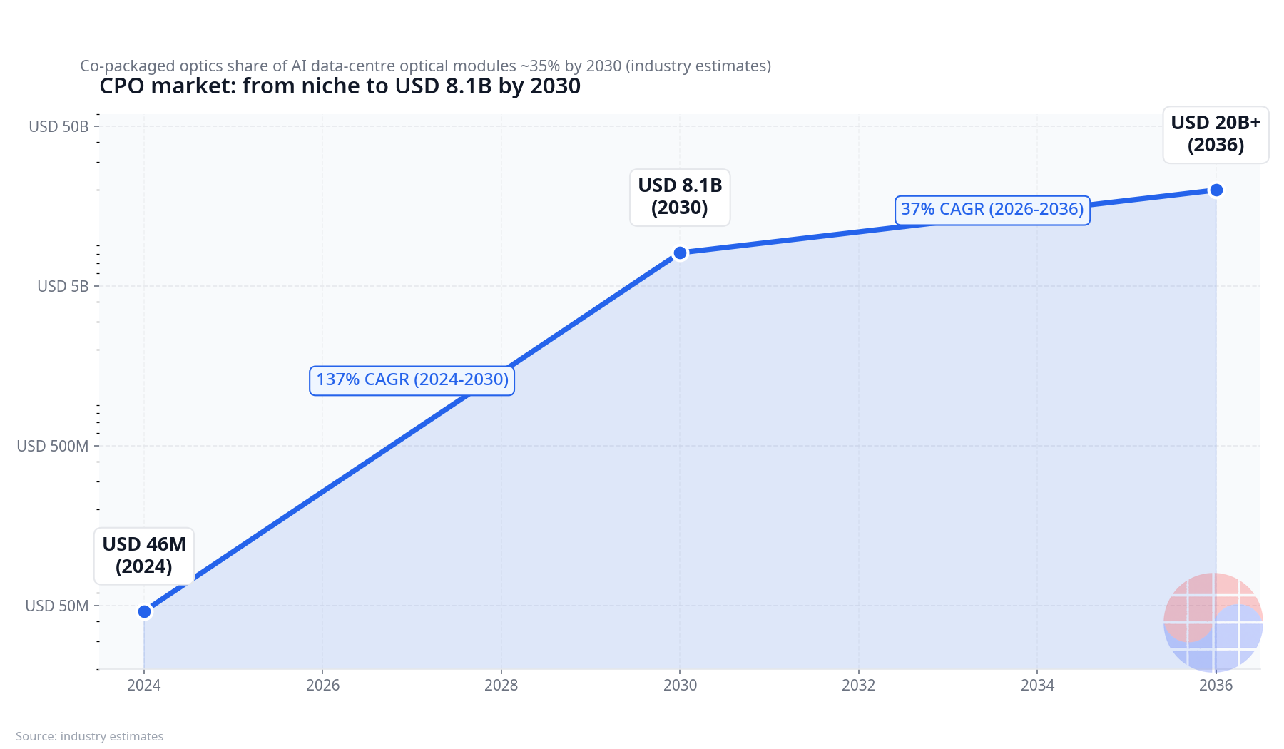
By 2030, roughly 35% of AI data-center optical modules are expected to be CPO. Hyperscaler CPO procurement is estimated at USD 2–4B annually in 2026–2028. This is not a "possible future" — purchase orders are already flowing.
Competitive Positioning: Who Defines the Architecture Takes the Margin
TSMC's COUPE (Compact Universal Photonic Engine) is close to the de facto standard of the CPO ecosystem. It entered volume production in 2026 and underpins NVIDIA's Quantum-X InfiniBand switches (H1 2026, 115 Tb/s per switch) and Spectrum-X Photonics Ethernet switches (H2 2026). Broadcom's Tomahawk 6-Davisson (102.4 Tb/s) also runs on COUPE. The Micro Ring Modulator jointly designed by NVIDIA and TSMC delivers 200 Gbps PAM4 per wavelength — the industry's densest single-channel bandwidth.
The business meaning is clear. TSMC has claimed the "architecture definer" position in CPO, just as it did with CoWoS. Whoever defines the architecture gets the design rules, the packaging path, and the supply chain stacked on top — and pricing power follows. In advanced packaging, TSMC holds 72.5% versus Samsung's 5.9%, per MTN-cited figures — a reminder of how narrow the latecomer's seat is. (These are MTN-cited figures, not independently audited statistics.)
| TSMC (COUPE) | Samsung Foundry | |
|---|---|---|
| Volume timing | 2026 (ramping) | Photonic IC manufacturing targeted 2027 |
| Anchor products | NVIDIA Quantum-X/Spectrum-X, Broadcom Tomahawk 6 | Alpha customer validation; targeting Coherent, Lumentum |
| Packaging linkage | SoIC-X hybrid bonding + CoWoS pathway | Advanced-packaging combination planned |
| Turnkey CPO target | — | 2029 |
| Advanced packaging share (MTN-cited) | 72.5% | 5.9% |
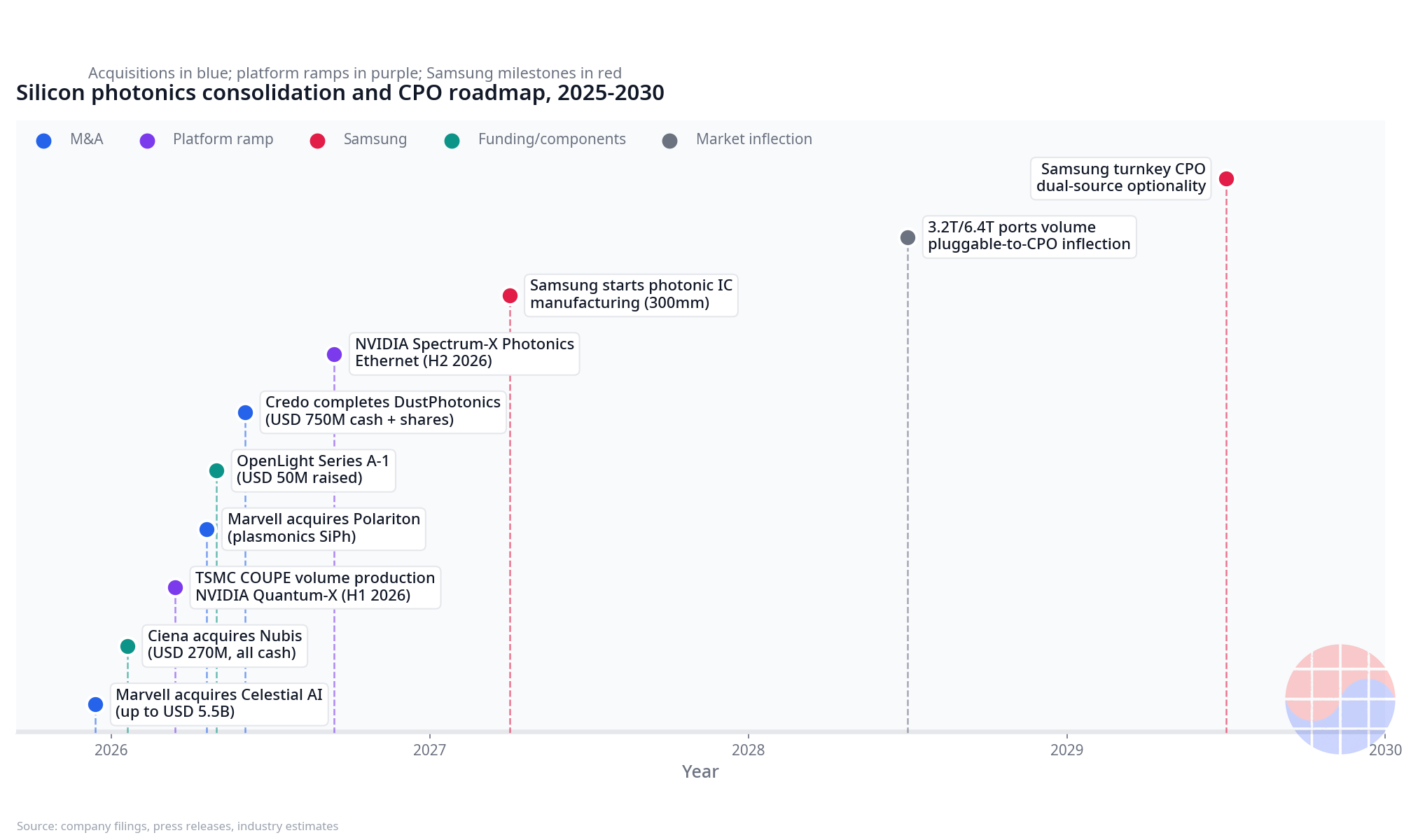
Samsung is not empty-handed. Its silicon photonics PDK is complete, it has a 300mm platform, and reports say it has won a major optical-module order. If the 2029 turnkey CPO roadmap materializes, Samsung becomes TSMC's only alternative. The value of that "alternative" is the subject of the next section.
Cost Structure: Why Pay USD 750M for a PIC?
The 2026 silicon photonics M&A wave shows where the money flows.
| Timing | Deal | Value | Significance |
|---|---|---|---|
| Dec 2025 | Marvell → Celestial AI | Up to USD 5.5B | Largest silicon photonics startup exit |
| Jan 2026 | Ciena → Nubis Communications | USD 270M (all cash) | CPO/NPO optical engines |
| Apr 2026 | Marvell → Polariton Technologies | Undisclosed | Plasmonics modulation for 3.2T+ |
| Apr 2026 | OpenLight Series A-1 | USD 50M (USD 84M total) | Open silicon photonics PDK, 25+ users |
| May 2026 | Credo → DustPhotonics | USD 750M cash + shares | In-house SiPh PIC, vertical integration |
[Sources: company announcements — Marvell, Zacks, Photonics Spectra, OpenLight]
Credo's DustPhotonics acquisition is the textbook case. Credo designed SerDes and DSPs — the brains of optical transceivers — but sourced the silicon photonics PIC, the chip that converts electricity into light, from third parties. Buying DustPhotonics completed the full stack: copper cable → DSP → PIC → system integration. The stated rationale had three parts: reduce external supply dependence, accelerate product development, and improve cost structure at volume. The judgment: in the CPO era, pricing power goes to whoever holds the optical engine.
Marvell follows the same grammar. Celestial AI (up to USD 5.5B) bought the Photonic Fabric vision; Polariton (plasmonics-based modulation) bought device-level innovation for the 3.2T era. Plasmonics enables higher-density, ultra-low-energy parallel optical links versus conventional silicon photonics.
The laser layer is a separate oligopoly. In CPO architecture, the optical engine cannot generate light itself — it needs an external light source injecting continuous-wave light. The global supply of high-power lasers that operate at 70–85°C next to a GPU package is effectively a Lumentum + Coherent duopoly. That is why NVIDIA took USD 2B of strategic equity in each, plus multibillion-dollar purchase commitments — USD 4B total, the largest directed supply-chain bet NVIDIA has ever made.
Strategy Options: What Samsung Can Buy — and Must Buy
Samsung's options fall into three buckets.
First, PIC design assets. Credo's USD 750M for DustPhotonics is the price list. Samsung has the PDK and the 300mm platform, but proven PIC design portfolios and customer traction must be bought to save time. The acquisition premium is the price of time.
Second, laser and light-source capability. Lumentum/Coherent-class high-power lasers rarely come up for sale. Instead, Samsung's play is to lock them in as foundry customers. Binding Coherent and Lumentum as customers cracks the TSMC-centric supply chain.
Third, packaging integration. Samsung's real differentiator is the vertical combination of foundry + memory + advanced packaging. CPO only works when electronic ICs, photonic ICs, advanced packaging, external lasers, and fiber coupling move as one body. No single layer wins alone; the integrator across layers wins. IDM-style vertical integration is one of Samsung's few structural strengths.
The risks are equally clear. In HBM, Samsung was slow to respond to AI demand and ceded share. The "arrive late, pay up" pattern could repeat in silicon photonics. Samsung must also choose whether to make acquired assets compatible with the TSMC COUPE ecosystem (faster commercialization) or pursue an independent standard (differentiation) — both cost money.
Chase's Take
This story is not "Samsung makes optical chips." It is "the ownership war over the optical I/O layer has entered the M&A phase."
Review how AI chip margins were distributed over the past decade. NVIDIA defined the compute layer, the HBM trio defined the memory layer, TSMC defined the packaging layer. Each layer's definer captured most of that layer's margin. The fourth layer now opening is optical I/O. TSMC has already taken its seat with COUPE; NVIDIA with Quantum-X/Spectrum-X and USD 4B of supply-chain investment. Samsung's acquisition review is a declaration that it will take a seat, late as it is.
Watch the number 2029. Samsung's turnkey CPO target coincides with market maturation. After the 2028 volume ramp of 3.2T/6.4T ports and the pluggable-to-CPO inflection, hyperscalers will demand dual sourcing. Nobody will accept single-foundry (TSMC) geopolitical and supply-chain risk. Samsung's 2029 turnkey CPO is not a share game — it is a dual-source option game. The value of an option scales with volatility (supply-chain risk), not with the underlying (share). The greater the geopolitical risk, the more Samsung's option is worth.
For investors, separate the valuation frames. Companies that in-house the optical engine (the Credo/Marvell/Ciena cohort) and pluggable module makers live under the same "optics" theme but are different stocks. The former eats the architecture-definition layer's margin; the latter eats the volume layer's cash flow. Mixing the two frames misprices the multiple.
Finally, the economics of the M&A premium. DustPhotonics raised a USD 24M Series B in 2024. The USD 750M+ acquisition price is more than 30x the capital raised. A bubble? If the CPO market reaches USD 8.1B by 2030 and the SiPh PIC layer is worth several billion, in-housing the PIC buys pricing power. The premium looks expensive, but through the lens of layer ownership it can be rational. Whatever Samsung pays now should be judged by the same yardstick. The goal is not to buy cheap — it is to buy the layer.
Implications
- Samsung: PIC design assets are the top acquisition target. Locking in Coherent and Lumentum as foundry customers is the lever against TSMC. The 2029 turnkey CPO's value is dual-source optionality, not share.
- TSMC: COUPE is CoWoS replayed. As the architecture definer, it absorbs most 2026–2028 CPO volume. The risk is single-source concentration and geopolitics.
- NVIDIA / Broadcom: the system-layer duopoly. NVIDIA seals the upstream with USD 4B of supply-chain investment; Broadcom is the default choice for the non-NVIDIA camp (Tomahawk 6 in volume).
- Investors: value optical-engine insiders and pluggable module makers on separate frames. Validate CPO on the timeline: revenue in 2026 → scale in 2027 → replacement inflection in 2028.
- Watch: Samsung's acquisition target announcement (price, assets), whether 2027 photonic IC manufacturing starts, and CPO penetration at the 2028 3.2T port ramp.
FAQ
Why is Samsung considering silicon photonics acquisitions?
To challenge TSMC's COUPE platform by combining foundry processes, memory, and advanced packaging. A senior Samsung official disclosed the acquisition review in an October 2026 MTN interview, with photonic IC manufacturing on 300mm wafers targeted for next year. With TSMC's roadmap one to two years ahead, M&A is a strategy to buy time. Source
How big is the CPO market?
Industry estimates put the CPO market at USD 46M in 2024 growing to USD 8.1B in 2030 (137% CAGR), exceeding USD 20B by 2036. Roughly 35% of AI data-center optical modules are expected to be CPO by 2030. Source
How do TSMC's COUPE and Samsung's plans differ?
TSMC COUPE is in volume production in 2026 and underpins NVIDIA Quantum-X/Spectrum-X and Broadcom Tomahawk 6. Samsung targets photonic IC manufacturing in 2027 and turnkey CPO in 2029, currently validating technology with an alpha customer. The gap is estimated at one to two years.
Why did Credo pay USD 750M for DustPhotonics?
To complete the full optical-connectivity stack by in-housing silicon photonics PICs alongside its SerDes and DSPs. The goals: reduce external supply dependence, accelerate development cycles, and improve cost structure at volume — a bet that CPO-era pricing power belongs to whoever holds the optical engine. Source
Disclaimer: This article summarizes public reporting and industry estimates as of October 18, 2026, and is not investment advice. Market figures are estimates that vary by source; M&A and roadmap details are based on company announcements and press coverage.
Related reading
- The Silicon Photonics Squeeze: Prepayments Reveal AI's Optical Bottleneck
- 400-Layer V-NAND and a 256TB SSD: The Storage Economics of Samsung's…
- Samsung and SK hynix Upgrade China NAND Fabs: 5 Facts Behind the…
- The Post-HBM Memory Hierarchy War: SK Hynix vs Samsung Battle to Define…
- Daily Silicon: TSMC at 73%, Samsung SF2: AI Foundry Revenue Up 29%