VLSI Korea
Daily Silicon: TSMC 3nm +15%, HBM4E Race Heats Up, Kioxia Hits 1000 Layers
🆓 무료 글 · 누구나 무료로 읽을 수 있는 글입니다 A practicing semiconductor engineer's daily read on global silicon news: At VLSI Symposium 2026, TSMC flexes pricing power with a 15% 3nm hike while SK Hynix and Samsung race to ship HBM4E samples ahead of schedule. Chase's Take — TSMC raising N3 prices 15% isn't inflation passthrough


🆓 무료 글 · 누구나 무료로 읽을 수 있는 글입니다
A practicing semiconductor engineer's daily read on global silicon news:
At VLSI Symposium 2026, TSMC flexes pricing power with a 15% 3nm hike while SK Hynix and Samsung race to ship HBM4E samples ahead of schedule.
Chase's Take — TSMC raising N3 prices 15% isn't inflation passthrough — it's a foundry monopolist telling AI customers there's nowhere else to go, and Samsung's 60%+ GAA yield and Intel's 18A-P risk production won't change that math until 2027 at the earliest. The HBM4E leapfrogging between SK Hynix and Samsung is more PR than substance right now — both are sampling, neither is shipping volume, and the real fight is who gets validated into Vera Rubin first. The Kioxia-SanDisk 1000-layer demo is the one I'd actually bet on long-term: wafer-to-wafer Cu hybrid bonding solves the cell-current and wafer-bow problems that have capped NAND stacking for years, even if 2031 production feels like a lifetime away. None of this changes the fact that retail consumers are getting squeezed out as NAND and DRAM supply gets routed straight to AI customers.
1. Kioxia and SanDisk Demo World-First 1,000-Layer 3D NAND at VLSI Symposium

TL;DR — Using an MSA-CBA structure with wafer-to-wafer Cu hybrid bonding, Kioxia and SanDisk demonstrated QLC operation at 1,000+ layers, solving cell-current degradation, wafer warpage, and oversized block issues that capped prior 3D NAND scaling. Mass production targeted for 2031.
Source: Kantenna — Kioxia and SanDisk Demo World-First 1,000-Layer 3D NAND at VLSI Symposium
2. US Awards SandboxAQ $500M to Find New Chipmaking Materials
TL;DR — The US government is funding NVIDIA-backed SandboxAQ with $500M and taking a minority stake to discover new semiconductor materials using AI and quantum simulation, a R&D track separate from CHIPS Act fab subsidies.
Source: Reuters — US Awards SandboxAQ $500M to Find New Chipmaking Materials
3. KB, Citi, Morgan Stanley Raise Samsung and SK Hynix Price Targets

TL;DR — Brokerages lifted targets on Samsung and SK Hynix citing an 'unprecedented growth' trajectory for 2026-2027 as DRAM prices stay strong; combined Q2 operating profit consensus tops KRW 150 trillion, with IBK and Citi forecasting Samsung operating profit of KRW 133-155 trillion.
Source: Etoday — KB, Citi, Morgan Stanley Raise Samsung and SK Hynix Price Targets
4. Silicon Motion: 'Retail SSD Market Has Almost Disappeared'
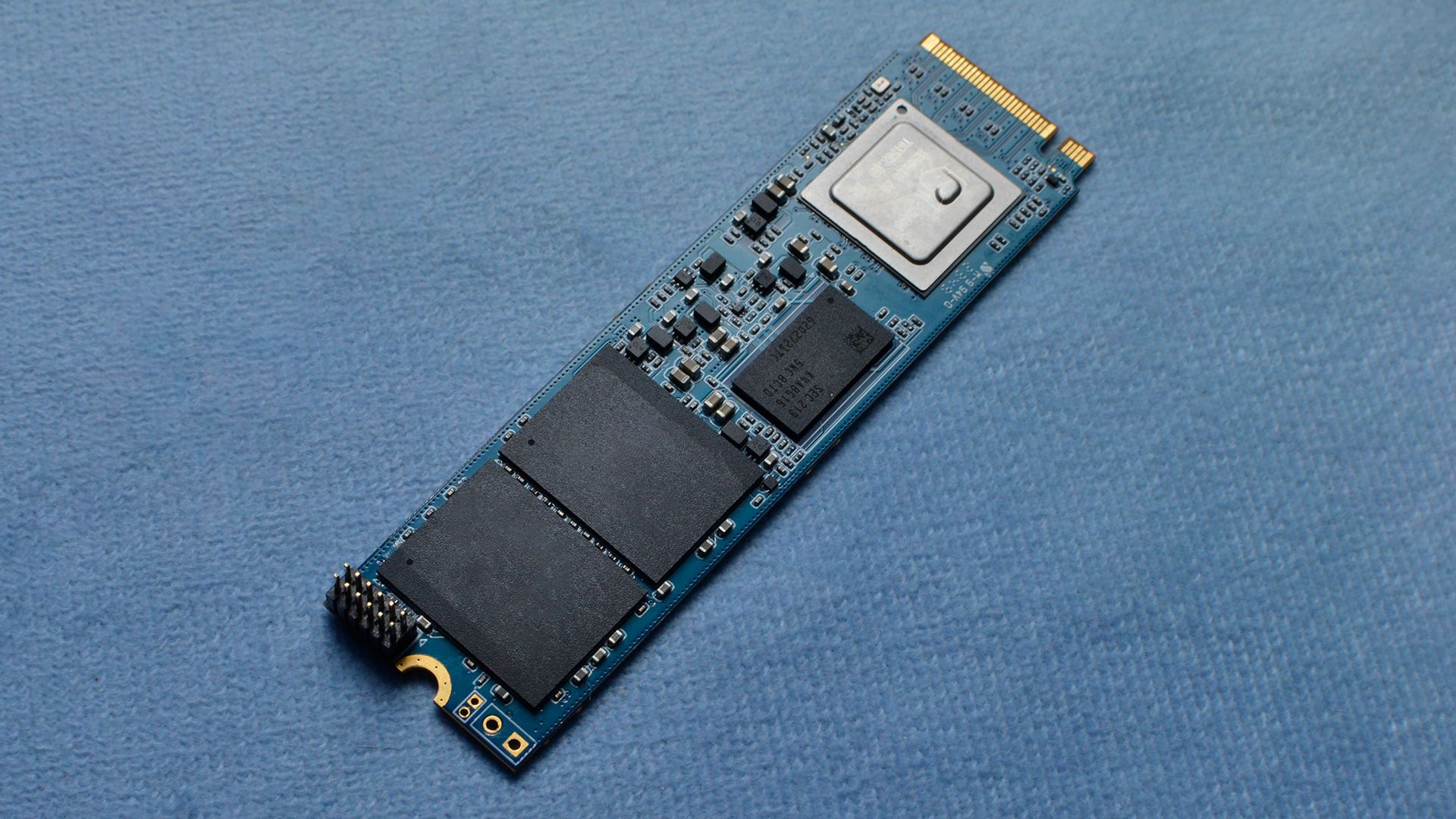
TL;DR — A Silicon Motion exec told Tom's Hardware that NAND makers funneling supply into enterprise/AI SSDs has pushed PC OEMs to buy third-party SSD controllers directly, squeezing retail/consumer SSDs out of the market amid tight NAND supply.
Source: Tom's Hardware — Silicon Motion: 'Retail SSD Market Has Almost Disappeared'
5. VLSI Symposium 2026: Hybrid Bonding, GAA, Backside Power, and 3D Stacking Highlights

TL;DR — Key papers at VLSI Symposium 2026 covered Cu hybrid bonding thermal characterization, GAA nanosheet reliability across TSMC N2/Samsung SF2P/Intel 18A, backside power delivery network IR-drop improvements, and 3D IC thermal management — five technology pillars shaping the post-Moore's Law roadmap.
Related reading
- Daily Silicon: Intel-Apple Chip Deal Surges 10%, Samsung-SK Cap Gap…
- Daily Silicon: Nomura SKH ₩4M, Kioxia 48x — and the Strike Is Coming
- Daily Silicon: Citi and KB Pile Into Memory Re-Rating, TSMC Adds $20B…
- Daily Silicon: AMD 2nm Defects to Samsung, SK hynix Tests Intel EMIB —…
- Daily Silicon: KOSPI Hits 9000, HBM4E Fires the Starting Gun